

Page 1
VITESSE
SEMICONDUCTOR CORPORATION
Data Sheet
VSC7810
Photodetector/Transimpedance Amplifier
Family for Optical Communication
G52145-0, Rev 4.1 Page 1
04/05/01
© VITESSE SEMICONDUCTOR CORPORATION • 741 Calle Plano • Camarillo, CA 93012
Tel: (800) VITESSE • FAX: (805) 987-5896 • Email: prodinfo@vitesse.com
Internet: www.vitesse.com
Features
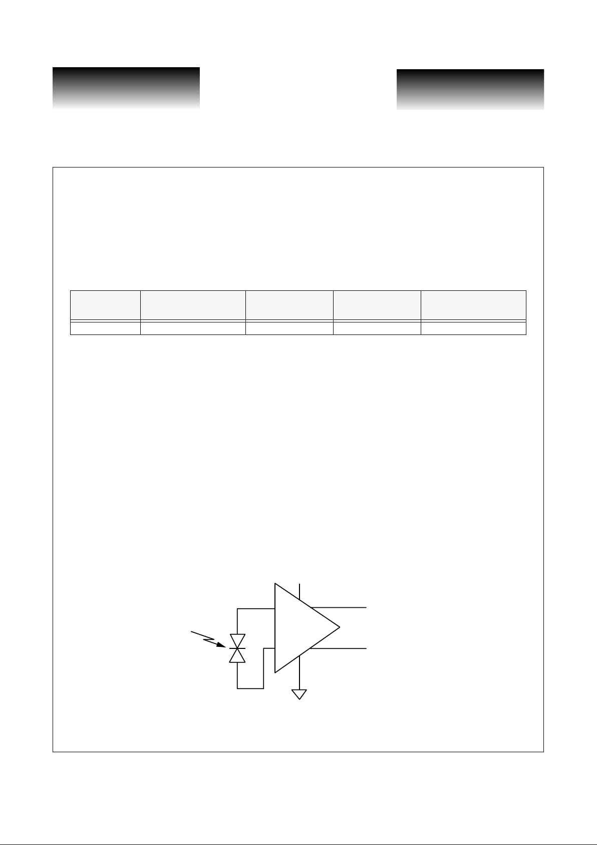
General Description
The VSC7810 integrated Photodetector/Transimpedance Amplifier provides a highly integrated solution
for converting light from a fiber optic communications channel into a differential output voltage. The benefits
of V itesse S emiconduct or’ s Galliu m Arsenide H-GaAs pr ocess are f ully ut ilized t o provid e very high bandwi dth
and low noise in a product with a large optically active area for easy alignment. The sensitivity, duty cycle distortion and jitter meet or exceed all Fibre Channel and Gigabit Ethernet application requirements. Par ts are
available in either die form, flat-windowed packages or in ball-l ens packag es.
By using a metal-semiconductor-metal (MSM) photodetector with a monolithic integrated transimpedance
amplifier , the input capacitance is lowered which allows for a la rger optically active area than in discrete photodetectors. Integration also allows superior tracking over process, temperature and voltage between the photodetector and the amplifier, resulting in higher performance. This part can easily be used in developing Fibre
Channel Electro-Optic Receivers which exhibit very high performance and ease of use.
VSC7810 Block Diagram
Part Number Data Rate
Bandwidth
(MHz)
Input Noise
(
µW rms)
Optically Active Area
(
µm diameter)
VSC7810 Full Speed: 1.25Gb/s 1200 0.45 100
• Integrated Photodetector/Transimpedance
Amplifier Optimized for High-Speed Optical
Communications Applications
• Integrated AGC
• Fibre Channel/Gigabit Ethernet Compatible
• High Bandwidth
• Low Input Noise Equivalent Power
• Large Optically Active Area
• Single 5V Power Supply
Both DOUTP and DOUTN are back-terminated to 25Ω.
Photodetector/Transimpedance Amplifier
DOUTP
DOUTN
+3.3V
GND
Page 2
VITESSE
SEMICONDUCTOR CORPORATION
Data Sheet
VSC7810
Photodetector/Transimpedance Amplifier
Family for Optical Communication
Page 2 G52145-0, Rev 4.1
04/05/01
© VITESSE SEMICONDUCTOR CORPORATION • 741 Ca ll e Pl an o • Camarillo, CA 93012
Tel: (800) VITESSE • FAX: (805) 987-5896 • Email: prodinfo@vitesse.com
Internet: www.vitesse.com
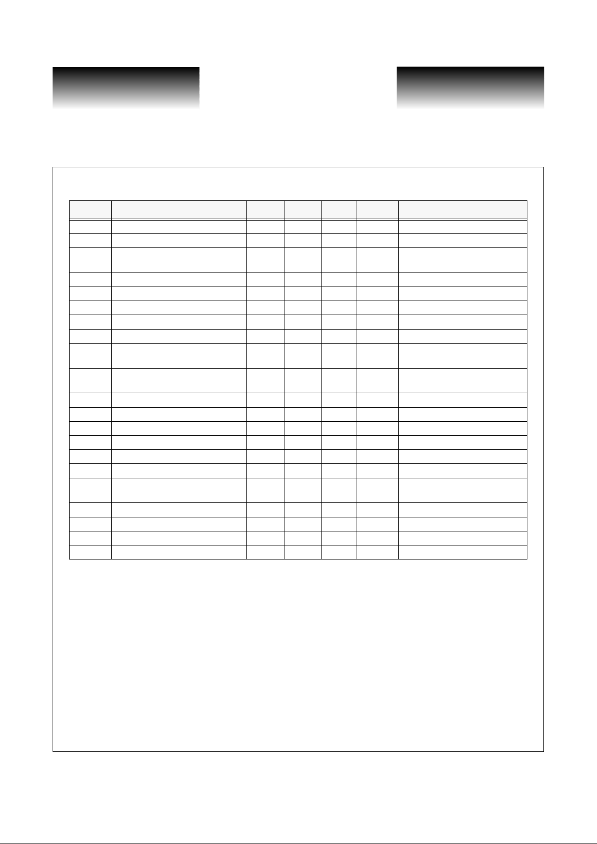
Table 1: Electro-Optical Specifications
(1)
Notes: (1) Specified over 0°C (ambient) to 70°C (case). (2) Typical conditions 25°C and 3.3V power supply. (3) See Note 1 in
Application Note 48. (4) P = Incident Optical Power (5) See Note 2 in Application Note 48.
Symbol Parameter Min Typ
(2)
Max Units Conditions
V
SS
Supply Voltage 4.5 5.0 5.5 V
I
DD
Supply Current 13 26 40 mA
PSRR Power Supply Rejection Ratio 35 - - dB
Frequencies up to 40MHz
(includes external filter).
λ Wavelength 700 840 850 nm
f
C
Low Frequency Cutoff - - 1.8 MHz -3dB, P = -15dBm @ 50MHz
(4)
BW Optical Modulation Bandwidth 800 1200 1300 MHz -3dB, P = -15dB m @ 50MHz
(4)
S Sensitivity -22 -25 -27 dBm 1.063Gb/s, BER10
-12(3)
R
O
Single-Ended Output Impedance 25 - 60 Ω
V
D
Differential Output Voltage 0.35 0.52 0.65 V
P = -4.5dBm,
R
LOAD
= 100Ω differenti a l
R
D
Differential Responsivity 0.8 2.2 - mV/µW
R
LOAD
= 100Ω
P = -15dBm @ 50MHz
V
DC
Output Bias Voltage 1.2 1.5 2.5 V
∆V
DC
Bias Offset Voltage - 40 150 mV
NEP
O
Input Noise Equivalent Power 0.35 0.45 0.93 µW rms P = 0mW
(5)
V
NO
Output Noise Volta ge 0.55 0.66 0.75 mV rms P = 0mW
(5)
DCD Duty Cycle Distortion - 1.5 4.5 % P = -4.5dBm
I
OUT
Output Drive Current 2.5 - 8 mA
PDJ Pattern Dependent Jitter 20 40 60 ps
P = -4.5dBm
+/-10% Voltage Window
Optically Active Area - 100 - µm Diameter
PPJ PP Jitter 120 160 200 ps P = -5dBm
t
R
Rise Time 310 355 400 ps 20%-80% P = -4.5dBm
t
F
Fall Time 280 325 370 ps 20%-80% P = -4.5dBm
Page 3
VITESSE
SEMICONDUCTOR CORPORATION
Data Sheet
VSC7810
Photodetector/Transimpedance Amplifier
Family for Optical Communication
G52145-0, Rev 4.1 Page 3
04/05/01
© VITESSE SEMICONDUCTOR CORPORATION • 741 Calle Plano • Camarillo, CA 93012
Tel: (800) VITESSE • FAX: (805) 987-5896 • Email: prodinfo@vitesse.com
Internet: www.vitesse.com
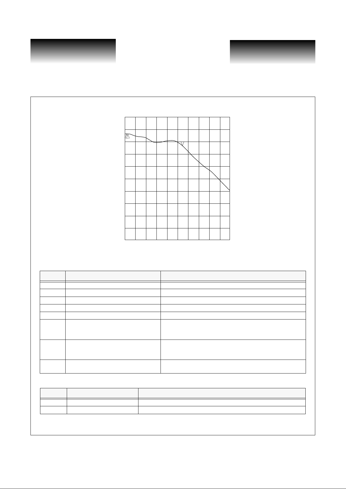
Figure 1: Amplifude vs. Frequency
Table 2: Absolute Maximum Ratings
Table 3: Recommended Operating Conditions
NOTE: (1) See Note 1 i n "Notes on M easurement Condi tions & Appl ications" se ction of thi s data sheet for extende d temperature range
operation.
Symbol Parameter Limits
V
SS
Power Supply 6V
T
STG
Storage Temperature -55°C to 125°C (case temp erat ure under bias)
H
STG
Storage Humidity 5 to 95% R.H. (includi ng con de n sa ti on)
H
OP
Operating Humidity 8 to 80% R.H. (excluding condensation)
P
INC
Incident Optical Power +3dBm
IS Impact Shock
500 G. Half Sine Wave
Pulse Duration 1 +/-0.5 ms
3 blows in each direction
V
IB
Vibration
20 > 2000 > 20 Hz, 10 Minutes
10 G. Peak Acceleration
4 Complete Cycles, 3 Perpendicular Axes
V
ESD
ESD Voltage on DOUTP, DOUTN, VSS,
GND
1500V
Symbol Parameter Limits
V
SS
Power Supply 4.5V to 5.5V (5V nominal)
T
OP
Operating Temperature 0°C (ambient) to 70° C (case) normal range and 90°C (case) extended range
(1)
1 096.795 514 MHz
1 000.150
1 999.700
21
3
Amplitude
Frequency (MHz)
Frequency response of VSC7810WB upper 3db frequency is measured with respect to response at 50 MHz
Page 4
VITESSE
SEMICONDUCTOR CORPORATION
Data Sheet
VSC7810
Photodetector/Transimpedance Amplifier
Family for Optical Communication
Page 4 G52145-0, Rev 4.1
04/05/01
© VITESSE SEMICONDUCTOR CORPORATION • 741 Ca ll e Pl an o • Camarillo, CA 93012
Tel: (800) VITESSE • FAX: (805) 987-5896 • Email: prodinfo@vitesse.com
Internet: www.vitesse.com
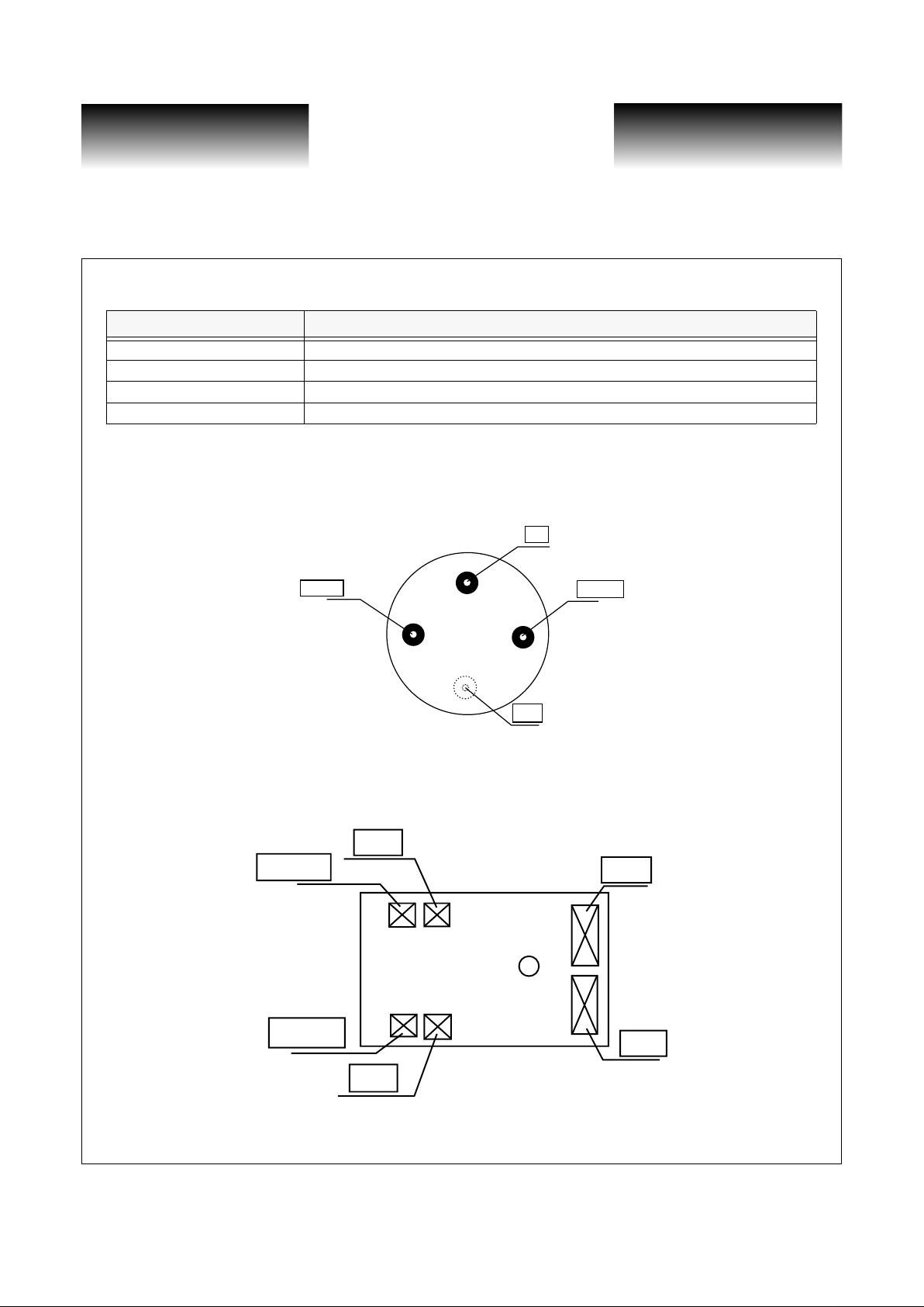
Table 4: Pin Table Specifications for Ball Lens Packages, Flat Window Packages and Bare Die
Note: Pin Diagram is identical for both TO-46 and TO-56 package styles.
Figure 2: Pin Diagram
Figure 3: Schematic View of Bare Die Pad Assignments
Symbol Description
DOUTP Data output normal (with reference to incident light)
DOUTN Data output complement (inverting, with reference to incident light)
VSS Power supply
GND Ground (package case)
DOUTP
DOUTN
GND
VSS
Bottom View
DOUTN
GND
GND
GND
VSS
DOUTP
Page 5
VITESSE
SEMICONDUCTOR CORPORATION
Data Sheet
VSC7810
Photodetector/Transimpedance Amplifier
Family for Optical Communication
G52145-0, Rev 4.1 Page 5
04/05/01
© VITESSE SEMICONDUCTOR CORPORATION • 741 Calle Plano • Camarillo, CA 93012
Tel: (800) VITESSE • FAX: (805) 987-5896 • Email: prodinfo@vitesse.com
Internet: www.vitesse.com
Temperature Dependence of Operating Parameters
This section describes the dependence of important operating parameters shown in Table 1 as a function of
die (or equivalently junction) tempeature and power supply. In order to relate the die temperature to an equivalent case temperature, the following thermal characteristics of the package are provided (note th at the therma l
conductivity is identical for TO-46 and TO-56 package styles.
Table 5: Thermal Resistance Calculation for TO-56 and TO-46 Packages
Chip Size 0.168cm x 0.104cm Thermal Path
Chip Area A 0.015cm
2
Die Height (T
DIE
)0.066cm
Epoxy Thickness (T
EPOXY
) 0.0076cm
Header Thickness (T
HEADER
)
(Average for TO-46 and TO-56 package)
0.115cm
Thermal Conductivities
K GaAs 0.55W/cm °C
K epoxy 0.0186W/cm °C
K kovar 0.17W/cm °C
θ
GaAs
K
GaAs
A
T
die
0.066
0.55 x 0.015
= 8 °C/W==
θ
epoxy
K
epoxy
A
T
epoxy
0.0076
0.0186 x 0.015
= 27.24 °C/W==
θ
kovar
K
kovar
A
T
kovar
0.12
0.17 x 0.015
= 47 °C/W==
θ
JC
= Thermal Resistance from Junction to Case = (8 + 27.24 + 47) = 82.24 °C/W
Example:
For VSC7810 at nominal supply current of 25mA and Vss = 5V
Temperature rise from junction to case = 0.025A x 5V x 82.24 °C/W = 10.28 °C
T
J
θ
GaAs
θ
EXPOXY
θ
KOVAR
T
C
Page 6

VITESSE
SEMICONDUCTOR CORPORATION
Data Sheet
VSC7810
Photodetector/Transimpedance Amplifier
Family for Optical Communication
Page 6 G52145-0, Rev 4.1
04/05/01
© VITESSE SEMICONDUCTOR CORPORATION • 741 Ca ll e Pl an o • Camarillo, CA 93012
Tel: (800) VITESSE • FAX: (805) 987-5896 • Email: prodinfo@vitesse.com
Internet: www.vitesse.com
Typical Operating Characteristics
35
33
31
29
27
25
23
21
19
17
15
Supply Current (mA)
IDD vs. Die Temperature
10 25 50 80 100
4.5V
5.5V
5V
Die Temperature ( C)
1400
1300
1200
1100
1000
900
800
-3dB Bandwidth (MHz)
Bandwidth vs. Die Temperature
10 25 50 80 100
5.5V
4.5V
5V
Die Temperature ( C)
3.00
2.80
2.60
2.40
2.20
2.00
1.80
1.60
1.40
1.20
1.00
Responsitivity (mV/µW)
Responsitivity vs. Die Temperature
(Small-Signal Optical Responsitivity at 850nm)
10 25 50 80 100
5.5V
4.5V
5V
Die Temperature ( C)
60
50
40
30
20
10
0
RMS Jitter (ps)
RMS Jitter with PRBS7 Data vs. Die Temperature
10 25 50 80 100
4.5V
5.5V
5V
Die Temperature ( C)
55
54
53
52
51
50
49
48
47
46
45
Duty-Cycle Distortion (%)
Duty-Cycle Distortion vs. Die Temperature
10 25 50 80 100
4.5V
5V
5.5V
Die Temperature ( C)
1.00
0.90
0.80
0.70
0.60
0.50
0.40
0.30
0.20
0.10
0.00
RMS Differential Output Noise Voltage (V)
RMS Differential Output Noise Voltage
vs. Die Temperature
10 25 50 80 100
5.5V
4.5V
5V
Die Temperature ( C)
Page 7

VITESSE
SEMICONDUCTOR CORPORATION
Data Sheet
VSC7810
Photodetector/Transimpedance Amplifier
Family for Optical Communication
G52145-0, Rev 4.1 Page 7
04/05/01
© VITESSE SEMICONDUCTOR CORPORATION • 741 Calle Plano • Camarillo, CA 93012
Tel: (800) VITESSE • FAX: (805) 987-5896 • Email: prodinfo@vitesse.com
Internet: www.vitesse.com
Figure 4: Eye Diagram
229mV
46mV
/div
not
trig'd
-231mV
39.34ns
183ps/div 41.17ns
Top
Btm
Lft
Rgt
15.56mV
-23.1mV
39.91ns
40.55ns
Mean
RMS∆
PkPk
Hits
40.23ns
25.98ps
146.4ps
6505
µ±1σ
µ±2σ
µ±3σ
Wfms
66.349%
97.54%
100%
1377
Left
39.90521ns
Right
40.54571ns
Page 8

VITESSE
SEMICONDUCTOR CORPORATION
Data Sheet
VSC7810
Photodetector/Transimpedance Amplifier
Family for Optical Communication
Page 8 G52145-0, Rev 4.1
04/05/01
© VITESSE SEMICONDUCTOR CORPORATION • 741 Ca ll e Pl an o • Camarillo, CA 93012
Tel: (800) VITESSE • FAX: (805) 987-5896 • Email: prodinfo@vitesse.com
Internet: www.vitesse.com
Notes on Measurement Conditions and Applications
Note 1: Noise Measurement Method
The VSC7810 is specified to operate in the following two ranges of temperature: (a) “normal” from 0°C
(ambient) to 70°C (case) and (b) “Extended” from 0°C (ambient) to 90°C (case). In the extended range, the
operating parameters are specified in Table 6.
Table 6: Specifications Under Extended Temperature Range of Operation
Note 2: Noise Measurement Method
The noise voltage, Vn, at t he o utput i s ref err ed back to the noise power at the input t hroug h t he responsivity
R (with R in volts/watts)
The bit error rate can be expressed as:
where ,
For a , the parameter Q = 7.
The sensitivity(s) at a bit error rate of is calculated as follows:
where the NEP is in units of milliwatts and S is in dBm, respectively.
Symbol Parameter Min Typ
(2)
Max Units Conditions
BW Optical Modulation Bandwidth 800 900 - MHz -3d B, P= -15dBm @ 50MHz
DUT
Board
P
2
3GHz BW
Hybrid Coupler
HP 437B
with
8481D
Power Sensor
Power Meter
RMS
Output
Noise
P
1
The noise voltage, (Vn), is calculated from the Output Noise Power, (Pn), into 50Ω.
Vn Pn 50•=
NEP
Vn
R
------ -=
BER 1
12–
×10=
1
12–
×10
e
(-Q
2
/
2)
√2πQ
.
(Q )
S = 10 log
10
NEP
1mW
,
BER =
Page 9

VITESSE
SEMICONDUCTOR CORPORATION
Data Sheet
VSC7810
Photodetector/Transimpedance Amplifier
Family for Optical Communication
G52145-0, Rev 4.1 Page 9
04/05/01
© VITESSE SEMICONDUCTOR CORPORATION • 741 Calle Plano • Camarillo, CA 93012
Tel: (800) VITESSE • FAX: (805) 987-5896 • Email: prodinfo@vitesse.com
Internet: www.vitesse.com
Note 3: Measurement Setup for Frequency Response
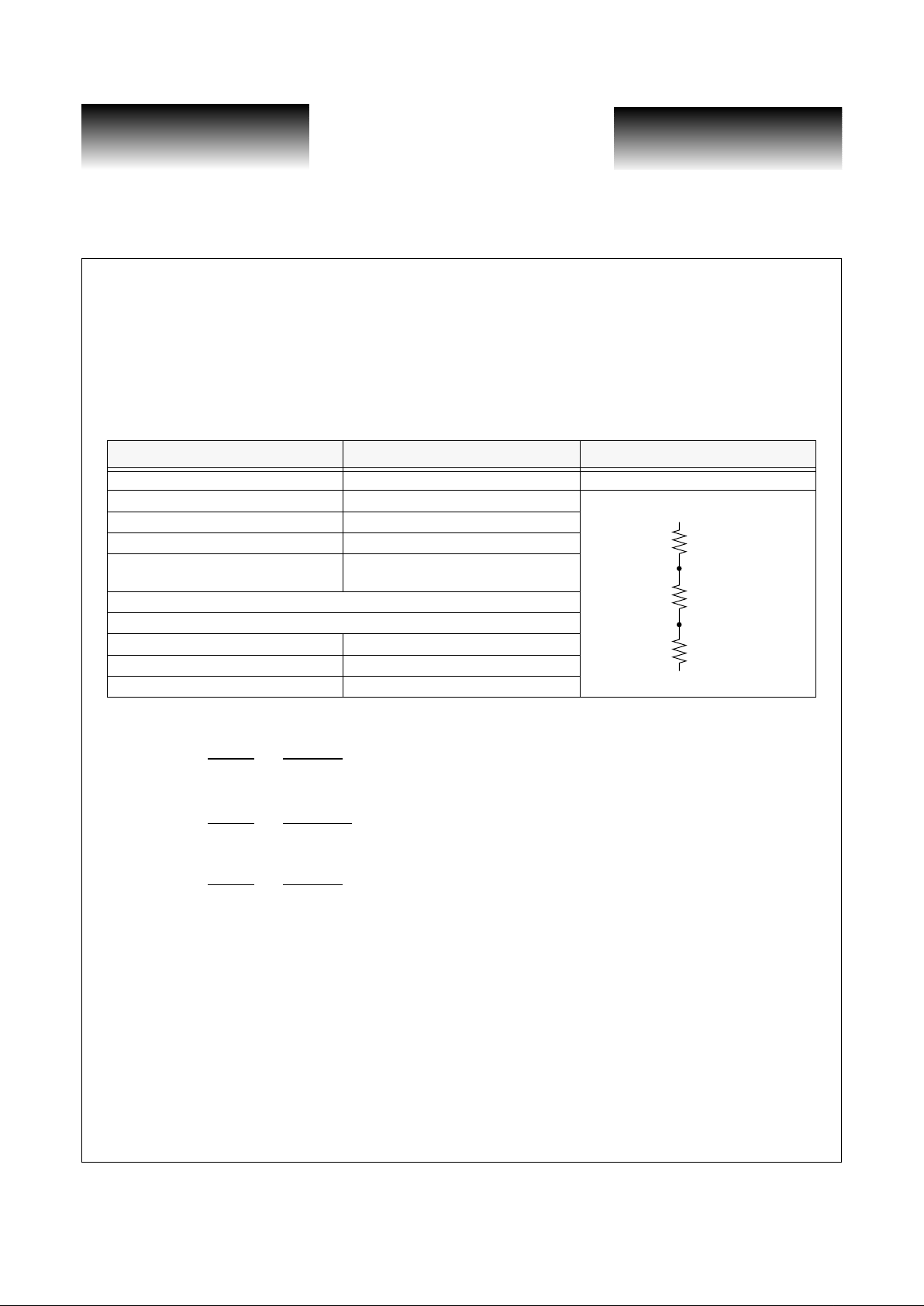
Note 4: Bias T Schematic
DC
1
AC
1
AC
2
DC
2
DUT
Hybrid
Coupler
Optical
Attenuator
Laser
Lightwave Component
Analyzer HP8702
Bias T
Bias T
Power
Supply
AC Out
DC Out
Signal
Page 10

VITESSE
SEMICONDUCTOR CORPORATION
Data Sheet
VSC7810
Photodetector/Transimpedance Amplifier
Family for Optical Communication
Page 10 G52145-0, Rev 4.1
04/05/01
© VITESSE SEMICONDUCTOR CORPORATION • 741 Ca ll e Pl an o • Camarillo, CA 93012
Tel: (800) VITESSE • FAX: (805) 987-5896 • Email: prodinfo@vitesse.com
Internet: www.vitesse.com
Package Information
(2x) 0.247
(2x) 0.1235
(2x) 0.18
1.04 ± 0.05
0.835
0.42
0.94
(4x) 0.055
(2x) 0.74
(2x) 0.29
0.35
(4x) 0.11
(2x) 0.15
1.68
1.48
1.58
0.05
DOUTN
GNDVSS
GND
DOUTP
GND
(4x) 0.365
(4x) 0.055
(6x) 0.11
0.05
φ0.1
VSC7809
0.05
0.05
Individual Die
Page 11

VITESSE
SEMICONDUCTOR CORPORATION
Data Sheet
VSC7810
Photodetector/Transimpedance Amplifier
Family for Optical Communication
G52145-0, Rev 4.1 Page 11
04/05/01
© VITESSE SEMICONDUCTOR CORPORATION • 741 Calle Plano • Camarillo, CA 93012
Tel: (800) VITESSE • FAX: (805) 987-5896 • Email: prodinfo@vitesse.com
Internet: www.vitesse.com
TO-56 Flat Window Package
Reference Isometric
Page 12

VITESSE
SEMICONDUCTOR CORPORATION
Data Sheet
VSC7810
Photodetector/Transimpedance Amplifier
Family for Optical Communication
Page 12 G52145-0, Rev 4.1
04/05/01
© VITESSE SEMICONDUCTOR CORPORATION • 741 Ca ll e Pl an o • Camarillo, CA 93012
Tel: (800) VITESSE • FAX: (805) 987-5896 • Email: prodinfo@vitesse.com
Internet: www.vitesse.com
Reference Isometric
TO-46 Ball Lens Package—7mm Lead Length
Page 13

VITESSE
SEMICONDUCTOR CORPORATION
Data Sheet
VSC7810
Photodetector/Transimpedance Amplifier
Family for Optical Communication
G52145-0, Rev 4.1 Page 13
04/05/01
© VITESSE SEMICONDUCTOR CORPORATION • 741 Calle Plano • Camarillo, CA 93012
Tel: (800) VITESSE • FAX: (805) 987-5896 • Email: prodinfo@vitesse.com
Internet: www.vitesse.com
TO-46 Ball Lens Package—13mm Lead Length
Reference Isometric
Page 14

VITESSE
SEMICONDUCTOR CORPORATION
Data Sheet
VSC7810
Photodetector/Transimpedance Amplifier
Family for Optical Communication
Page 14 G52145-0, Rev 4.1
04/05/01
© VITESSE SEMICONDUCTOR CORPORATION • 741 Ca ll e Pl an o • Camarillo, CA 93012
Tel: (800) VITESSE • FAX: (805) 987-5896 • Email: prodinfo@vitesse.com
Internet: www.vitesse.com
 Loading...