

Page 1

VITESSE
SEMICONDUCTOR CORPORATION
Advance Product Information
VSC7146
2.5Gb/s, 20-Bit Tr ansceiver
Features
• Speed Selectable Full-Duplex Transceiver:
- 1.06/2.12Gb/s for FibreChannel
- 1.25/2.5Gb/s for Gigabit Ethernet
• 20-Bit TTL Interface for Transmit and
Receive Data at 125MHz
• Monolithic Clock Synthesis and Clock
Recovery - No External Components
• 125MHz TTL Reference Clock
• Automatic Lock-to-R eference Function
• Suitable for Both Coaxi al and O pt i cal Link Applications
• Low Power Operation: 2.5 W max
• 80-Pin, 14mm Thermally-Enhanced EDQUAD
Package
• Single +3.3V Supply
General Description
The VSC7146 is a 2.5Gb/s Transceiver optimized for ease-of-use and efficiency in high-performance data
transmission systems. The VSC7146 accepts two 10-bit 8b/10b encoded transmit characters, latches them on
the rising edge of Transmit Byte Clock (TBC) and serializes the data onto the TX+/- differential outputs at a
baud rate, which is 20 times the TBC frequency. The VSC7146 also samples serial receive data on the RX+/differential inputs, recovers the clock and data, deserializes it onto two 10-bit receive characters, outputs a
recovered clocks at one-twentieth of the incoming baud rate and detects Fibre Channel “comma” characters.
The VSC7146 contai ns o n- ch ip Ph ase -Lo ck Loop (PLL ) c ircu itr y for sy nth esis o f th e bau d -rate tra nsm it cloc k,
and extraction of the clock from the received serial stream. These circuits are fully monolithic and require no
external components.
Block Diagram
EWRAP
20
R0:19
RBC
RBCN
COM_DET
EN_CDET
T0:19
TBC
REF
TXRATE
BCMN
Q D
125 MHz
20
125 MHz
Frame
Logic
D Q
Serial to
Parallel
÷
20
Comma
Detect
Parallel
to Serial
PLL Clock
Multiply (x20)
Retimed
Data
Recovered
Clock
2.5 Gb/s
Serial Data
2.5 GHz
Synthesized
Clock
Q D
Clock
Recovery
2:1
D Q
2.5 Gb/s
RX+
RX-
RXRATE
TX+
TX-
G52162-0, Rev. 2.7
8/28/00 741 Calle Plano, Camarillo, CA 93012 • 805/388-3700 • FAX: 805/987-5896
VITESSE SEMICONDUCTOR CORPORATION
Page 1
Page 2

VITESSE
SEMICONDUCTOR CORPORATION
2.5Gb/s, 20-Bit Transceiver
Advance Product Information
VSC7146
Functional Description
Clock Synthesizer
The VSC7146 clock synthesizer multiplies the 125MHz reference frequency provided on the REF input by
20 to achieve a baud rate clock at 2.5GHz. The clock synthesizer contains a fully monolithic PLL which
requires no external components. An additional 125MHz clock, TBC, should be provided to clock in the data
bus. Since TBC is only used for the purpose of clocking data in, it is not required to have the same jitter
constraints as REF. REF clock and TBC should preserve certain phase margins and be of the same frequency.
Serializer
The VSC7146 accepts TTL input data as two parallel 10-bit characters on the T[0:19] bus which is latched
into the input latch on the rising edge of a 125MHz clock at TBC. This data will be serialized and transmitted on
the TX differential outputs at a baud rate of 20 times the frequency of the TBC input, with bit T0 transmitted
first. User data should be enco ded f or t ra nsmissi on us in g th e 8B/ 10B block code described in th e Fi br e Ch annel
specification, or an equivalent, edge rich, DC-balanced code. If EWRAP is HIGH, the transmitter will be
disabled with TX+ HIGH and TX- LOW. If EWRAP is LOW, the transmitter outputs serialized data. The
phases of REF clock and TBC can be identical, but there is a phase relationship between the two input clocks
which must be maintained.
Transmission Character Interface
In Fibre Channel, an encoded byte is 10 bits and is referred to as a transmission character. The 20-bit
interface on the VSC7146 corresponds to two transmission characters. This mapping is shown in Figure 1.
Figure 1: Transmission Order and Mapping to Fibre Channel Character
Parallel Data Bits 19 18 17 16 15 14 13 12 11 10 09 08 07 06 05 04 03 02 01 00
8B/10B Bit Position j h g f i e d c b a j h g f i e d c b a
V alid “Comma” Position 1111100
Last Data Bit Transm itted
Clock Recovery
The VSC7146 accepts different ial hi gh-spe ed seri al inpu ts o n th e RX+/RX- pins, (when E WRAP is LOW),
extracts the clock and retimes t he dat a. The serial bit stream shoul d be encoded so as to provide DC b ala nce a nd
limited run length by a Fibre Channel-compatible 8B/10B transmitter or equivalent. The VSC7146 clock
recovery circuitry is completely monolithic and requires no external components. For proper operation, the
baud rate of the data stream to be recovered should be within 200ppm of twenty times the REF frequency. This
allows oscillators on either end of the link to be 125MHz +/- 100ppm.
First Data Bit Transmitted
Page 2
741 Calle Plano, Camarillo, CA 93012 • 805/388-3700 • FAX: 805/987-5896 8/28/00
VITESSE SEMICONDUCTOR CORPORATION
G52162-0 Rev. 2.7
Page 3

VITESSE
SEMICONDUCTOR CORPORATION
Advance Product Information
VSC7146
Deserializer
The retimed serial bit stream is converted into two 10-bit parallel out put characters. The VSC7146 provides
a TTL recovered clock, RBC, at one twentieth of the serial baud rate. The clock is generated by dividing down
the high-speed clock which is phase-locked to the serial data. The serial data is retimed by the internal highspeed clock, and deseriali zed. The resul ting par allel dat a will be cap ture d by the adjo ining proto col logic on t he
rising edge of RBC.
If serial input data is not present, or does not meet the required baud rate, the VSC7146 will continue to
produce a recovered clock and RBC will automatically lock to the REF reference clock. This eliminates the
need for a Lock-to-Reference input pin and simplifies the support software for that function.
Word Alignment
The VSC7146 provides 7-bit Fibre Chan nel “comma” charact er recognition and dat a word al ignment. Word
synchronization is enabled by asserting EN_CDET HIGH. When synchronization is enabled, the VSC7146
constantly examines the serial data for the presence of the Fibre Channel “comma” character. This pattern is
“0011111XXX”, where the leading zero corresponds to the first bit received. The “comma” sequence is not
contained in any normal 8B/10B coded data character or pair of adjacent characters. It occurs only within
special characters, known as K28.1, K28.5 and K28.7, which are defined specifically for synchronization in
Fibre Channel systems. Improper alignment of the “comma” character is defined as either of the following
conditions:
2.5Gb/s, 20-Bit Tr ansceiver
1) The “comma” is not aligned within the 10-bit transmission character such that T0...T6 = “0011111.”
2) The “comma” straddles the boundary between two 10-bit transmission characters.
When EN_CDET is HIGH and an improperly aligned “comma” is encountered, the internal data is shifted
in such a manner that the “comma” character is aligned properly in R[0:6] as shown in Figure 1. This results in
proper character and word alignment. When the parallel data alignment changes in response to a improperly
aligned “comma” pattern, some data which would have been presented on the parallel output port may be lost.
However, the synchronization character and subsequent data will be output correctly and properly aligned.
When EN_CDET is L OW, the current alignme nt o f th e seri al d ata is mai nt ain ed i nde fini te ly, regardless of data
pattern.
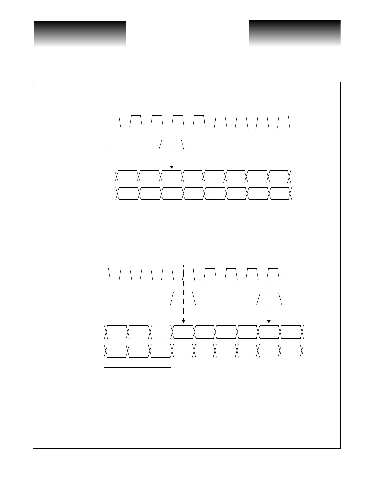
On encountering a “comma” character, COM_DET is driven HIGH to inform the user that realignment of
the parallel data field may have occurred. The COM_DET pulse is presented simultaneously with the “comma”
character and has a duration equal t o the data. Th e COM_DET signal is timed such t hat it can be captured b y the
adjoining protocol logic on the rising edge of RBC. Functional waveforms for synchronization are shown in
Figure 2 and Figure 3. Figure 2 shows the case when a “comma” character is detected and no phase adjustment
is necessary. It illustrates the position of the COM_DET pulse in relation to the “comma” character on R[0:6].
Figure 3 shows the case where the K28.5 is detected, but it is out-of-phase and a change in the output data
alignment is required. Note that up to three characters prior to the “comma” character may be corrupted by the
realignment process.
G52162-0, Rev. 2.7
8/28/00 741 Calle Plano, Camarillo, CA 93012 • 805/388-3700 • FAX: 805/987-5896
VITESSE SEMICONDUCTOR CORPORATION
Page 3
Page 4
VITESSE
SEMICONDUCTOR CORPORATION
2.5Gb/s, 20-Bit Transceiver
Figure 2: Detection of a Properly Aligned “Comma” Character
RBCN
COM_DET
R[0:9]
R[10:19]
TChar: 10 bit Transmission Character
Figure 3: Detection and Resynchronization of an Improperly Aligned “Comma” Character
Advance Product Information
VSC7146
K28.5 TChar TChar TChar
TChar TChar TChar TChar
Receiving T wo Consecutive K28.5+TChar Transmission Words
RBCN
COM_DET
R[0:9]
R[10:19]
Potentially Corrupted
K28.5 TChar TChar TChar K28.5 TChar
TChar TChar TChar TChar TChar TChar
Page 4
741 Calle Plano, Camarillo, CA 93012 • 805/388-3700 • FAX: 805/987-5896 8/28/00
VITESSE SEMICONDUCTOR CORPORATION
G52162-0 Rev. 2.7
Page 5

VITESSE
SEMICONDUCTOR CORPORATION
Advance Product Information
VSC7146
Dual Data Rate Operation
The VSC7146 performs at two data rates, full-speed (2.5 Gb/s on the serial link, 125MHz on the parallel
20-bit data bus) and half-speed (1.25 Gb/s on the serial link, 62.5 Mb/s on the parallel 20-bit data bus). To
accommodate for this, the user is provided with 3 signal pins for data rate control: TXRATE, RXRATE and
BCMN. The usage of these signals is as follows:
If BCMN = 0 (Backwards Compatibility Mode), TXRATE controls both the serializer and deserializer
speeds. TXRATE should be HIGH for full-speed operation and LOW for half-speed operation.
If BCMN = 1, TXRATE controls the serializer speed and RXRATE controls the deserializer speed.
TXRATE and/or RXRATE must be HIGH for full-speed operation and/or LOW for half-speed operation.
Table 1: Data Rate
BCMN TXRate RXRate Description
0 1 X Both serializer and deserializer run at full-speed.
0 0 X Both serializer and deserializer run at half-speed.
1 0 0 Both serializer and deserial izer run at half-speed.
1 0 1 Serializer is run at half-speed and deserializer is run at full-speed.
1 1 0 Serializer is run at full-speed and deserializer is run at half-spee d.
1 1 1 Both serializer and deserializer run at full-speed.
2.5Gb/s, 20-Bit Tr ansceiver
For “comma” character (K28.5) detection, it is recommen ded no t to use differing RXRATE inputs to actual
RX rate data reception, as shown in the Table 2 (assumes EN_CDET = 1):
Table 2: Comma Detect
RXRate
0 Half-Speed 2.5Gb/s Will only detect 00/00/11/11/11/11/11 pattern as “comma”. Do not use.
0 Half-Speed 1.25Gb/s Normal detection operation.
1 Full-Speed 2.5Gb/s Normal detection operation.
1 Full-Speed 1.25Gb/s Will detect false characters (e.g., those that include “0111”) as “comma”. Do not use.
Similarly, it is recommended not to use differing TXRATE inputs to actual TX rate data reception. The
T[19:0] data bus, TBC and REF clock inputs must be at 125Mb/s rates if TXRATE = 1 and 62.5Mb/s if
TXRATE = 0. It is important to note tha t the PLL will not lock otherwise.
Along with the 20-bit data input to the serializer, the user will also have to send the appropriate transmit
byte clock signal (TBC)—that is, 125MHz when TXRATE = 1 and 62.5MHz when TXRATE = 0. REF and
TBC should be frequency-locked in all cases and should maintain a certain phase relationship as shown in
Figure 6. The output recovered clocks (RBC/RBCN), the output deserialized data (R[19:0]) and the internal
VCO high-speed clock mul tiplier will be automatically adjusted by the TXRAT E a nd RXRATE signals.
The baud rate of the data stream to be recovered in the deserializer should be within 200ppm of the REF
frequency. In other words:
RX+/- Actual
Data Rate
F
REF TX–
F
– 200ppm≤
REF RX–
“Comma” Detect
G52162-0, Rev. 2.7
8/28/00 741 Calle Plano, Camarillo, CA 93012 • 805/388-3700 • FAX: 805/987-5896
VITESSE SEMICONDUCTOR CORPORATION
Page 5
Page 6
VITESSE
SEMICONDUCTOR CORPORATION
Advance Product Information
2.5Gb/s, 20-Bit Transceiver
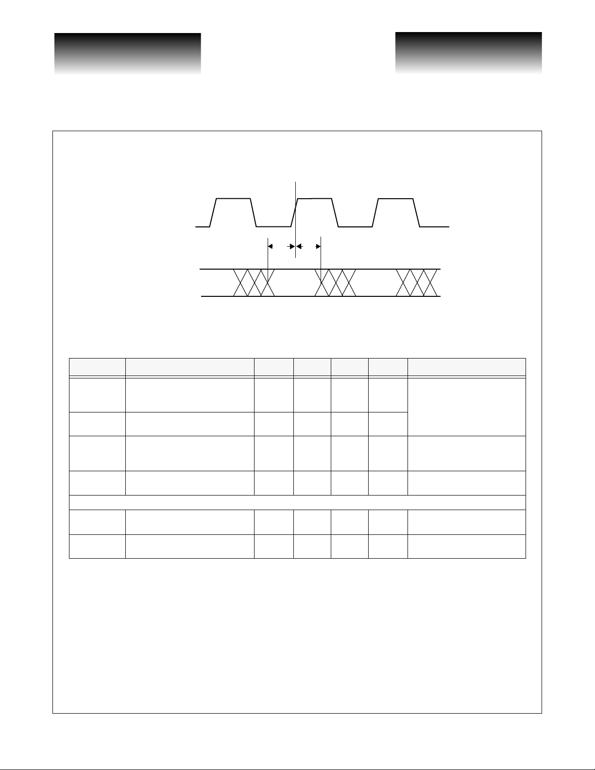
Figure 4: Transmit Timing Waveforms
TBC
T
T
T[0:19]
20-Bit Data
Data Valid
Data Valid
Table 3: Transmit AC Characteristics
Parameters Description Min Typ Max Units Conditions
T
1
T
2
T
SDR,TSDF
T
LA T
T[0:19] setup time to the rising
edge of TBC
T[0:19] hold time after the rising
edge of TBC
TX+/TX- rise and fall time — 160 ps
Latency from rising edge of TBC
to T0 appearing on TX+ TX-
1.5 —ns
1.0 — ns
24 bc
+1ns
Transmitter Output Jitter Allocation
T
RJ
T
DJ
Serial data output random jitter
(RMS)
Serial data output deterministic
jitter (p-p)
— 5 7.5 ps RMS, tested on a sample basis.
—2530ps
2
1
Data Valid
Measured between the valid
data level of T[0:19] to the
1.4V point of TBC.
20% to 80% into 50Ω load to
VSS.
Tested on a sample basis.
45 bc
+1ns
Bit
Clock
Bit clock periods
(PLL locked)
Peak-to-peak, tested on a
sample basis.
VSC7146
Page 6
741 Calle Plano, Camarillo, CA 93012 • 805/388-3700 • FAX: 805/987-5896 8/28/00
VITESSE SEMICONDUCTOR CORPORATION
G52162-0 Rev. 2.7
Page 7

VITESSE
SEMICONDUCTOR CORPORATION
Advance Product Information
VSC7146
RBCN
RBC
R[0:19] and
COM_DET
Table 4: Receive AC Characteristics
Paramete
rs
T
1
T
2
T
3
, T
T
R1
, T
T
R2
R
LA T
T
RBC
DC RBC duty cycle 40% 60% period
T
LOCK
Data or COM_DET valid prior to
RBCN rise
Data or COM_DET valid after
RBCN rise
Time difference between RBC and
RBCN edges
RBC/RBCN rise and fall time 0.6 2.0 ns
F1
R[0:19], COM_DET rise and fall
F2
time
Latency from RX to R[0:19]
RBC period
Data acquisition lock time @
2.5Gb/s
Description Min. Max. Units Conditions
Figure 5: Receive Timing Waveforms
T
T
3
3
T
—ns
—ns
56bc+
2ns
8.1
16.2
Data Valid
T
1
Data Valid Data Valid
1.0
2.0
5.0
10.0
—1 ns
0.7 2.4 ns
36bc+
2ns
7.9
15.8
—1250
2
Bit
Clocks
ns
Bit
Clocks
2.5Gb/s, 20-Bit Transceiver
Measured between the 1.4V point of
RBCN and a valid le vel of R[0:19] or
COM_DET . All outp uts driving 10pF lo ad.
The spec on top relects RXMODE=1 and
the bottom one reflects RXMODE=0.
Between V
10pF load.
Between V
10pF load.
When locked to valid data.
The spec on top relects RXMODE=1 and
the bottom one reflects RXMODE=0.
T e ste d on a sample basis. 95% pro bab ility
of lock.
(max) and VIH(min), into
IL
(max) and VIH(min), into
IL
G52162-0, Rev. 2.7
8/28/00 741 Calle Plano, Camarillo, CA 93012 • 805/388-3700 • FAX: 805/987-5896
VITESSE SEMICONDUCTOR CORPORATION
Page 7
Page 8

VITESSE
SEMICONDUCTOR CORPORATION
Advance Product Information
2.5Gb/s, 20-Bit Transceiver
Figure 6: TBC and REF Timing Waveforms
T
H
TBC
REF
T
L
REF
127
63.5
T
2
REF and TBC must not have their
opposing edges c oincident within
2.0ns of each other.
Measured from falling edge of REF to rising
edge of TBC.
Measured from falling edge of REF to rising
edge of TBC.
Range over which both transmit and receive
MHz
reference clock s on any link may be centered.
The figure on top relects TXMODE=1 and the
bottom one reflects TXMODE=0.
- RX
|TX
TBC
Low is measured from VIL(max) to VIL(max),
High is measured from V
Min measurement refers to TXMODE=0 and
Max measurement refers to TXMODE=1.
Between VIL(max) and VIH(min).
T
1
TBC
Table 5: TBC and REF Requirements
Parameters Description Min Max Units Conditions
T
T
FR Frequency Range
FO Frequency Offset
T
L,TH
DC TBC and REF duty cycle 40 60 % Measured at 1.5V.
T
RCR,TRCF
Necessary lag time between TBC
1
and REF
Necessary lead time between
2
TBC and REF
Pulse Width, Low / High
TBC and REF rise and fall time
—2.0 ns
—2.0 ns
105
52.5
−
100 +100 ppm
4.5 2.5 ns
0.6 1.5 ns
VIH(min)
VIL(max)
|
TBC
VSC7146
(min) to VIH(min).
IH
Page 8
741 Calle Plano, Camarillo, CA 93012 • 805/388-3700 • FAX: 805/987-5896 8/28/00
VITESSE SEMICONDUCTOR CORPORATION
G52162-0 Rev. 2.7
Page 9

VITESSE
SEMICONDUCTOR CORPORATION
Advance Product Information
VSC7146
Serial Input Rise and Fall Time TTL Input and Output Rise and Fall Time
2.5Gb/s, 20-Bit Transceiver
Figure 7: Parametric Measurement Information
V
80%
20%
T
r
T
f
T
r
T
f
Receiver Input Eye Diagram Jitter Tolerance Mask
Bit Time
Amplitude
Eye Width%
IH(min)
V
IL(max)
Serial Output Load
Z0 = 50Ω
Parametric Test Load Circuit
50Ω
V
-0.6V
DD
TTL AC Output Load
10 pF
G52162-0, Rev. 2.7
8/28/00 741 Calle Plano, Camarillo, CA 93012 • 805/388-3700 • FAX: 805/987-5896
VITESSE SEMICONDUCTOR CORPORATION
Page 9
Page 10

VITESSE
SEMICONDUCTOR CORPORATION
2.5Gb/s, 20-Bit Transceiver
Absolute Maximum Ratings
Power Supply Voltage, (VDD)
DC Input Voltage (Differential inputs)
DC Input Voltage (TTL inputs)
DC Output Voltage (TTL Outputs)
Output Current (TTL Outputs)...................................................................................................................
Output Current (Differential Outputs)
Case Temperature Under Bias
Storage Temperature
Relative Humidity (Storage)......................................................................................0% - 95% (Non-condensing)
Relative Humidity (Operating)................................................................................................................8% - 80%
Maximum Input ESD (Human Body Model)............................................................................................1500V
NOTES: (1) CAUTION: Str e s s es lis te d under “Absol ute Maximum Ratings” may b e ap plied to device s o ne a t a time without ca us -
ing permanent damage. Functionality at or above the values listed is not implied.Exposure to these values for extended
periods may affect device reliability.
(2) High-speed PECL receiver inputs only are rated at 700V.
....................................................................................................................−
...........................................................................................................−
.............................................................................................. −
.......................................................................................−
.....................................................................................................−
(1)
..................................................................................−
............................................................................................±50mA
Advance Product Information
VSC7146
0.5V to +4V
0.5V to V
0.5V to V
0.5V to V
o
C to +125oC
55
o
65
C to +150oC
+0.5V
DD
DD
+ 0.5V
DD
±50mA
+0.5V
(2)
Recommended Operating Conditions
Power Supply Voltage, (VDD)................................................................................................................+3.3V+5%
Power Supply Noise, (V
Operating Temperature Range ............................................................. 0
)........................................................................100mVp-p from 100Hz to TBD MHz
DD
o
C Ambient to +90oC Case Temperature
Page 10
741 Calle Plano, Camarillo, CA 93012 • 805/388-3700 • FAX: 805/987-5896 8/28/00
VITESSE SEMICONDUCTOR CORPORATION
G52162-0 Rev. 2.7
Page 11

VITESSE
SEMICONDUCTOR CORPORATION
Advance Product Information
VSC7146
DC Characteristics
(Over recommended operating conditions)
2.5Gb/s, 20-Bit Transceiver
Parameters Description Min Typ Max Units Conditions
∆V
∆V
V
V
OUT50
OUT75
∆V
V
V
V
I
I
I
P
Z
OH
OL
IN
IH
IL
DD
DD
Z
(1)
IH
IL
D
O
I
Output HIGH voltage (TTL) 2.4 ——VIOH = −1.0 mA
Output LOW voltage (TTL) — — 0.5 V IOL = +1.0 mA
Serial output absolute voltage
(1)
differential peak-to-peak swing
(TX+/TX-)
Serial output absolute voltage
(1)
differential peak-to-peak swing
(TX+/TX-)
Serial input absolute voltage
differential peak-to-peak swing
(RX+/RX-)
Input HIGH voltage (TTL) 2.0 — 5.5 V
Input LOW voltage (TTL) 0 — 0.8 V
Input HIGH current (TTL) — 1000 µAVIN = 2.4 V
Input LOW current (TTL) — — -500 µAVIN = 0.5 V
Supply voltage 3.14 — 3.47 V +3.3V± 5%
Power dissipation — 1.8 2.6 W Outputs open, VDD = VDD max
Supply current — 550 750 mA Outputs open, VDD = VDD max
Output resistance (TX) — 50 — Ω
Input resistance (RX) — 50 — Ω
600 1100 2000 mV
600 1100 2000 mV
400 — 2200 mV
Driving a 50Ω transmission line
(TX+ - TX-)
Driving a 75Ω transmission line
(TX+ - TX-)
(RX+ - RX-)
Note: (1) Refer to Application Note, AN-37, for differential measurement techniques.
G52162-0, Rev. 2.7
8/28/00 741 Calle Plano, Camarillo, CA 93012 • 805/388-3700 • FAX: 805/987-5896
VITESSE SEMICONDUCTOR CORPORATION
Page 11
Page 12

VITESSE
SEMICONDUCTOR CORPORATION
2.5Gb/s, 20-Bit Transceiver
INPUT
Figure 8: Input Structures
+3.3 V
V
DD
Current
Limit
R
R
GND
TTL Inputs
Advance Product Information
VSC7146
Figure 9: High-Speed I/O T ermination Scheme
Transmitter
Output
50 50
VSC7146
No external resistor terminations are necessary on the high-speed I/O
50Ω Transmission Line
50
50
Off-Chip
Receiver
Input
V
BB
VSC7146
Page 12
741 Calle Plano, Camarillo, CA 93012 • 805/388-3700 • FAX: 805/987-5896 8/28/00
VITESSE SEMICONDUCTOR CORPORATION
G52162-0 Rev. 2.7
Page 13

VITESSE
SEMICONDUCTOR CORPORATION
Advance Product Information
VSC7146
Package Pin Descriptions
(T op View)
VDD
T0
T10
T1
T11
T2
VSS
T12
T3
T13
T4
T14
VDD
T5
T15
T6
T16
T7
T17
T8
1
3
5
7
9
11
13
15
17
19
TEST4
21
2.5Gb/s, 20-Bit Transceiver
Figure 10: Pin Diagram
VSSP
RXRATE
VDD
79
TX-
VDDP
75
25
TX+
VDDP
73
27
VSSA
29
VSS
VDDA
71
31
RX+
RX-
VDD
67
69
33
VDD
35
R0
65
R10
372339
R1
R11
637761
VSST
VSST
59
57
55
53
51
49
47
45
43
41
R2
R12
R3
R13
R4
R14
VDDT
R5
R15
R6
R16
R7
R17
VDDT
R8
R18
R9
R19
VSST
NOTES:
G52162-0, Rev. 2.7
VDD
T18T9T19
VSS
VSS
REF
Heat Sink is not connected electricall y. It should not be connected el ectrically by the us er.
Pin 80 has changed from SLOOP in previous versions of th e spe c t o TEST4. Tie this pin to VSS.
VITESSE SEMICONDUCTOR CORPORATION
TBC
VSS
TEST2
TEST1
BCMN
TEST3
TXRATE
EN_CDET
RBC
VSST
EWRAP
RBCN
COM_DET
8/28/00 741 Calle Plano, Camarillo, CA 93012 • 805/388-3700 • FAX: 805/987-5896
Page 13
Page 14

VITESSE
SEMICONDUCTOR CORPORATION
2.5Gb/s, 20-Bit Transceiver
Table 6: Pin Identifications
Pin # Name Description
2, 4, 6, 9, 11, 14, 16, 18, 20,
23, 3, 5, 8, 10, 12, 15, 17,
19, 22, 24
26 REF
28 TBC
74,75 TX+, TX-
65, 63, 59, 57, 55, 52, 50,
48, 45, 43, 64, 62, 58, 56,
54, 51, 49, 47, 44, 42
35 TXRATE
79 RXRATE
29 BCMN
36 EWRAP
68, 67 RX+, RX-
38, 39
34 EN_CDET
37 COM_DET
T[0:19]
R[0:19]
RBC, RBCN
Advance Product Information
VSC7146
INPUTS - TTL:
Transmit Data Bus, Bit 0 through Bit 19. 20-bit Transmit Character. Parallel data on
this bus is clocked in on the rising edge of TBC. The data bit corresponding to T0 is
transmitted first.
INPUT - TTL:
Reference Clock. REF goes to the PLL/CMU circuitry and is multiplied 20 times
INPUT - TTL:
Transmit Byte Clock.
This rising edge of this clock latches T[0:19] into the input register and provides the
reference clock at 1/20th of the baud rate to the PLL.
OUTPUTS - Differential (AC-coupling recommended):
Transmitter Serial Outputs. These pins output the serialized transmit data when
EWRAP is LOW. When EWRAP is HIGH, TX+ is HIGH and TX- is LOW.
OUTPUTS - TTL:
Receive Data Bus, Bits 0 thru 19. 20-bit received character. Parallel data on this bus
can be sampled on the rising edge of RBC. R0 is the first bit received on RX+/RX-.
INPUT - TTL:
Transmitter Dual Rate Select or. LOW for half-speed operation (1.25Gb/s). HI GH for
full-speed operation (2.5 Gbps).
INPUT - TTL:
Receiver Dual Rate Selector. LOW for half-speed operation (1.25Gb/s). HIGH for
full-speed operation (2.5Gb/s).
INPUT - TTL:
Backwards Compatibility Mode Selector. LOW to allow operation in previous version compatibility (no separate rate controls for transmitter and receiver). HIGH to
allow operation with separate rate controls for transmitter and receiver.
INPUT - TTL:
Enable Internal WRAP Mode. LOW for Normal Operation. When HIGH, an internal
loopback path from the transmitter to the receiver is enabled, TX+ = HIGH and TXis LOW.
INPUTS - Differential (AC-coupling recommended):
Receive Serial Inputs. The receiver inputs when EWRAP is LOW.
OUTPUT - TTL:
Recovered Byte Cl ock. Recovered clock and complement derived from 1/20
RX+/- data rate. The rising edge of RBC corresponds to a new word on R[0:19].
INPUT - TTL: ENable Comma DETect. Enables COM_DET and word resynchronization when HIGH. When LOW, keeps current word alignment and disables
COM_DET.
OUTPUT - TTL:
COMma DETect. This output goes HIGH to indicate that R[0:6] contains a “comma”
character (‘0011111’). COM_DET can be sampled on the rising edge of RBC.
th
of the
Page 14
741 Calle Plano, Camarillo, CA 93012 • 805/388-3700 • FAX: 805/987-5896 8/28/00
VITESSE SEMICONDUCTOR CORPORATION
G52162-0 Rev. 2.7
Page 15

VITESSE
SEMICONDUCTOR CORPORATION
Advance Product Information
VSC7146
Pin # Name Description
31, 32, 33
80 TEST4
1, 13,21, 66, 69,78 VDD Digital Power Supply, +3.3V.
46, 53 VDDT TTL Power Supply, +3.3V.
71 VDDA Analog Power Supply, +3.3V.
73, 76 VDDP High-Speed Outpu t Driver Power Supply, +3.3V
7, 25, 27, 30, 70 VSS Digita l Ground, 0V.
40, 41, 60, 61 VSST TTL Ground, 0V.
72 VSSA Analog Ground, 0V.
77 VSSP High-Speed Output Driver Ground, 0V.
TEST1,
TEST2,
TEST3
2.5Gb/s, 20-Bit Transceiver
TEST Pins
For internal Vitesse use only.
Customers should tie TEST1, TEST2 and TEST3 to V
TEST Pins
For internal Vitesse use only.
Customers should tie TEST4 to V
.
SS
DD
.
G52162-0, Rev. 2.7
8/28/00 741 Calle Plano, Camarillo, CA 93012 • 805/388-3700 • FAX: 805/987-5896
VITESSE SEMICONDUCTOR CORPORATION
Page 15
Page 16

VITESSE
SEMICONDUCTOR CORPORATION
2.5Gb/s, 20-Bit Transceiver
Package Information
G
80 61
1
20
21 40
Advance Product Information
VSC7146
F
Item 14 mm Tolerance
A2.35 MAX
D 2.00 +0.10/-0.05
60
IH
41
E0.30 ±.05
F 17.20 ±.25
G 14.00 ±.10
H 17.20 ±.25
I 14.00 ±.10
J 0.88 +.15/-.10
K0.65BASIC
10° TYP
A
10° TYP
NOTES:
Drawing not to scale.
All units in mm unless otherwise noted.
K
A
0.17 MAX.
EXPOSED HEATSINK
+
6.85
.50 DIA
-
HEATSINK INTRUSION
.0127 MAX
D
0.30 RAD. TYP.
0.20 RAD. TYP.
0.25
0° - 8°
J
STANDOFF
0.25 MAX.
0.102 MAX LEAD
COPLANARITY
E
Page 16
741 Calle Plano, Camarillo, CA 93012 • 805/388-3700 • FAX: 805/987-5896 8/28/00
VITESSE SEMICONDUCTOR CORPORATION
G52162-0 Rev. 2.7
Page 17

VITESSE
SEMICONDUCTOR CORPORATION
Advance Product Information
VSC7146
2.5Gb/s, 20-Bit Transceiver
Package Thermal Characteristics
The VSC7146 is packaged in an 80-pin, 14mm thermally-enhanced EDQUAD with an internal heat
spreader. These packages use industry-standard EIAJ footprints, which have been enhanced to improve thermal
dissipation. The construction of the packages are as shown in Figure 11. The VSC7146 is designed to operate
with a case temperature up to 90
Insulator
Table 7: Thermal Resistance
o
C. The user must guarantee that the temperature specification is not violated.
Figure 11: Package Cross Section
Exposed Heat Slug
Wire Bond
Thermal Epoxy
Plastic Molding Compound
Lead
Die
Symbol Description Value Units
o
C/W
o
C/W
o
C/W
o
C/W
o
C/W
o
C/W
θ
θ
ca-100
θ
ca-200
θ
ca-400
θ
ca-600
θ
ca-0
jc
Thermal resistance from junction-to-case 2.5
Thermal resistance from case-to-ambient, st ill air 35
Thermal resistance from case-to-ambient, 100 LFPM air 29
Thermal resistance from case-to-ambient, 200 LFPM air 26
Thermal resistance from case-to-ambient, 400 LFPM air 22
Thermal resistance from case-to-ambient, 600 LFPM air 19
G52162-0, Rev. 2.7
8/28/00 741 Calle Plano, Camarillo, CA 93012 • 805/388-3700 • FAX: 805/987-5896
VITESSE SEMICONDUCTOR CORPORATION
Page 17
Page 18

VITESSE
SEMICONDUCTOR CORPORATION
2.5Gb/s, 20-Bit Transceiver
Ordering Information
The part number for this product is formed by a combination of the device number and the package style:
Device Type
2.5 Gb/s, 20-Bit Transceiver
VSC7146
Advance Product Information
VSC7146
xx
Package
RH: 80-Pin, 14x14mm EDQUAD
Notice
This document contains information about a new product during its fabrication or early sampling phase of
development. The information contained in this document is based on design targets, simulation results or early
prototype test results. Characteristic data and other specifications are subject to change without notice.
Therefore, the reader is cautioned to confirm that this data sheet is current prior to design or order placement.
Warning
Vitesse Semiconductor Corporation’s products are not intended for use in life support appliances, devices
or systems. Use of a Vitesse product in such applications without written consent is prohibited.
Page 18
741 Calle Plano, Camarillo, CA 93012 • 805/388-3700 • FAX: 805/987-5896 8/28/00
VITESSE SEMICONDUCTOR CORPORATION
G52162-0 Rev. 2.7
Page 19

VITESSE
SEMICONDUCTOR CORPORATION
Advance Product Information
VSC7146
Revision History:
1.0 Initial Release
1.1 Fix Fig 5, Add Figure 10, New numbers for Power Supply, Dissipation, Zi/Zo/Ri/Ro & Termination.
1.2 Added T
1.3 Filled in TBA’s, package pinout, pin description, dual-mode description. For internal CDR.
2.0 Post CDR. Rev.A target spec.
2.1 Pre-CDR. Rev. B target spec.
2.2 Post-CDR. Rev. B API. Removed reliability table. Changed BCLK name to TBC.
2.2.1 Removed 50 ohm termination wording in table on page 10.
2.3 Modified title and features section to reflect dual speed.
2.4 Added facility loop-back (SLOOP) and speed negotiation port (TXRATE, RXRATE, BCMN) features.
Modified pinout list and diagram accordingly.
Modified spec as per ICR results.
Changed package type from QZ to RH.
, Power Supply Noise, Pinout Diagram, Different Thermals, Added Reliability
rj/Tdj
2.5Gb/s, 20-Bit Transceiver
2.5 Removed facility loop-back (SLOOP) feature. Changed pin# 80 from SLOOP to TEST4.
Modified Figures 2 and 3 to better reflect RBCN relationship with output data R[0:19].
Modified RBCN vs. R bus timing as per characterization findings.
2.6 Revised max Idd to 750 ma, max power to 2.6 W; Modified ESD rating on p.10; removed “Vitesse
Confidential”
2.7Added typ column to Table 3: TRJ:added typ 5 ps, changed max from 5ps to 7.5ps; TDJ: added typ
25ps. Corrected grammatical/typo errors and corrected inconsistencies. Updated format. Removed marking
information.
G52162-0, Rev. 2.7
8/28/00 741 Calle Plano, Camarillo, CA 93012 • 805/388-3700 • FAX: 805/987-5896
VITESSE SEMICONDUCTOR CORPORATION
Page 19
 Loading...