

Page 1
®
VSC7132
VITESSE
SEMICONDUCTOR CORPORATION
Preliminary Data Sheet
Link Replicator for Fibre
Channel, Gigabit Ethernet and HDTV
Features
• Replicates Fibre Channel, Gigabit Ethernet and
HDTV Links
• T11 Fibre Channel Compliant at 1.0625Gb/s
• IEEE802.3z Gigabit Ethernet Compliant at 1.25Gb/s
• SMPTE-292M Compliant at 1.485Gb/s
General Description
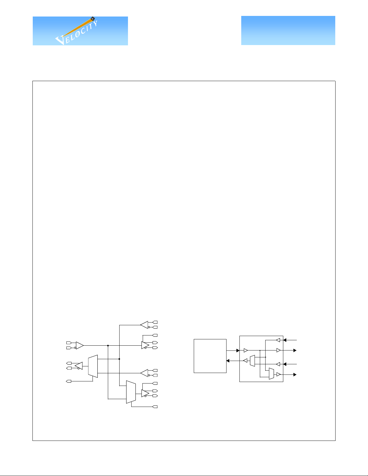
The VSC7132 is a high performance serial Link Replicator for applications in Fibre Channel (1.0625Gb/s),
Gigabit Ethernet (1.25Gb/s) and HDTV (1.485Gb/s). A serializer/deserializer, such as the VSC7123, would
normally be connected to the IN+/- and OUT+/- ports in order to provide duplicate links on the IN0/OUT0 and
IN1/OUT1 ports. A popular application is for Line Cards using serial links from a SerDes (VSC7123) or Serial
Backplane IC (VSC7211) where the VSC7132 provides redundant, hot-swappable links to redundant Switch
Fabric Cards. Another common application is in Host Adapters which require an internal and an external connector where the VSC7132 steers serial data between the SerDes (VSC7123) and the two connectors.
IN is sent to both OUT0 and OUT1 whose buffers are enabled when OE0 and OE1 are HIGH. OUT1 can
select between IN and IN0. OUT can select between IN0 and IN1.
In Link Replicator applications, such as the Line Card to Switch Card links, IN is transmitted to both OUT0
and OUT1, which either IN0 or IN1 is selected at OUT. In Host Adaptor applications, IN goes to OUT0 (an
internal connector) which returns data on IN0. IN0 is looped to OUT1 (an external connector) which returns
data on IN1 and then back to the SerDes on OUT.
• No External Components Required
• 0.4W Maximum Power Dissipation
• 3.3V Power Supply
• 28-Pin, 4.4 x 9.7mm TSSOP Package
G52243-0, Rev 3.0 Page 1
9/21/00
VSC7132 Block Diagram
IN+
IN-
OUT+
OUT-
MUX
0
1
0
1
© VITESSE SEMICONDUCTOR CORPORATION • 741 Calle Plano • Camarillo, CA 93012
Tel: (800)-VITESSE • FAX: (805) 987-5896 • Email: prodinfo@vitesse.com
IN0+
IN0-
OE0
OUT0+
OUT0-
SERDES
IN1+
IN1-
OE1
OUT1+
OUT1MUX1
Internet: www.vitesse.com
VSC7123
TX
RX
VSC7132
LOOP0
LOOP1
Page 2

®
VSC7132
VITESSE
SEMICONDUCTOR CORPORATION
Link Replicator for Fibre
Preliminary Datasheet
Channel, Gigabit Ethernet and HDTV
Figure 1: Timing Waveforms
IN+/IN0+/IN1+/-
OUT+/OUT0+/OUT1+/-
T
1
T
1
Table 1: AC Characteristics (Over recommended operating conditions)
Parameters Description Min Typ Max Units Conditions
F Operating frequency range 1.0 1.5 Gb/s
T
TR, T
T
1
J
Flow-through propagation delay 7.0 ns
Serial data rise and fall time — 300 ps
F
Deterministic jitter added to serial
input
— 30 ps p-p
— 40 ps p-p
T
J
Delay from any input to any
output.
20% to 80%, tested on a
sample basis
1.0 - 1.25 Gb/s. Measured on
K28.5+, K28.5- pattern
1.25 - 1.5 Gb/s. Measured on
K28.5+, K28.5- pattern
Table 2: DC Characteristics (Over recommended operating conditions)
Parameters Description Min Typ Max Units Conditions
V
IH(TTL)
V
IL(TTL)
I
IH(TTL)
I
IL(TTL)
V
DD
I
DD
P
D
(1)
DV
IN
DV
OUT50
DV
OUT75
NOTE: (1) Refer to Application Note, AN-37, for differential measurement techniques.
Page 2 G52243-0, Rev 3.0
Input HIGH voltage 2.0 — 5.5 V
Input LOW voltage 0 — 0.8 V
Input HIGH current — — 100 mA VIN = 2.4 V
Input LOW current — — –100 mA VIN = 0.5 V
Supply voltage 3.14 — 3.47 V VDD = 3.30V + 5%
Supply current — — 150 mA
Power dissipation 275 400 mW
Receiver differential peak-to-peak
Input Sensitivity, IN, IN0, IN1
Output differential peak-to-peak
(1)
voltage swing, OUT, OUT0, OUT1
Output differential peak-to-peak
(1)
voltage swing, OUT, OUT0, OUT1
© VITESSE SEMICONDUCTOR CORPORATION • 741 Calle Plano • Camarillo, CA 93012
Tel: (800)-VITESSE • FAX: (805) 987-5896 • Email: prodinfo@vitesse.com
300 2600 mVp-p
1000 — 2200 mVp-p 50Ω to VDD – 2.0 V
1200 2200 mVp-p 75Ω to VDD – 2.0 V
Internet: www.vitesse.com
Outputs open, VDD = VDD
max
Outputs open, VDD = VDD
max
AC-Coupled.
Internally biased at VDD/2
9/21/00
Page 3
®
VSC7132
VITESSE
SEMICONDUCTOR CORPORATION
Preliminary Data Sheet
Link Replicator for Fibre
Channel, Gigabit Ethernet and HDTV
Absolute Maximum Ratings
TTL Power Supply Voltage (VDD) .....................................................................................................0.5V to +4V
PECL DC Input Voltage (V
TTL DC Input Voltage (V
).............................................................................................................–0.5V to VDD +0.5V
INP
) .........................................................................................................................–0.5V to +5.5V
INT
DC Voltage Applied to Outputs for High Output State (V
PECL Output Current, (I
) (DC, Output High)..................................................................................................... –50mA
OUT
Case Temperature Under Bias (TC) .............................................................................................................–55oC to +125oC
Storage Temperature (T
)..........................................................................................................................–65oC to +150oC
STG
Recommended Operating Conditions
Power Supply Voltage (VDD).....................................................................................................+3.14V to +3.47V
Ambient Operating Temperature Range (T) ....................................................................................0oC to +70oC
NOTES: (1) CAUTION: Stresses listed under “Absolute Maximum Ratings” may be applied to devices one at a time without caus-
ing permanent damage. Functionality at or above the values listed is not implied. Exposure to these values for extended
periods may affect device reliability.
(2) Vitesse guarantees the functional and parametric operation of the part under“Recommended Operating Conditions”
except where specifically noted in the AC and DC Parametric Tables
(1)
)...............................................–0.5V to VDD + 0.5V
IN TTL
(2)
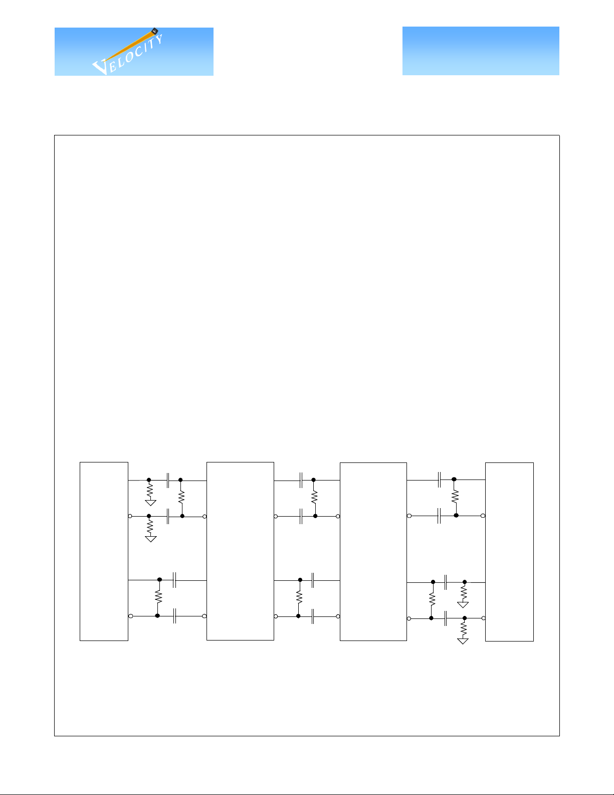
Figure 2: Application Example: VSC7123 and VSC7132 Interconnect
TX+
TX-
VSC7123
RX+
RX-
“R” is 180Ω for 100Ω differential traces or 267Ω for 150Ω differential traces.
“RT” matches the differential impedance of the link.
.01
R
.01
R
.01
RT
.01
I+
RT
I-
VSC7132
O+
O-
O1+
O1-
I1+
I1-
.01
RT
.01
.01
RT
.01
I1+
I1-
VSC7132
O1+
O1-
O+
O-
.01
.01
I+
RT
I-
.01
.01
RX+
RT
RX-
VSC7123
TX+
R
TX-
R
G52243-0, Rev 3.0 Page 3
9/21/00
© VITESSE SEMICONDUCTOR CORPORATION • 741 Calle Plano • Camarillo, CA 93012
Tel: (800)-VITESSE • FAX: (805) 987-5896 • Email: prodinfo@vitesse.com
Internet: www.vitesse.com
Page 4

®
VSC7132
VITESSE
SEMICONDUCTOR CORPORATION
Link Replicator for Fibre
Channel, Gigabit Ethernet and HDTV
Package Pin Descriptions
VDDP0
OE0
MUX
VSS
IN+
IN-
VSS
OE1
VDD
VDDP
OUT+
OUT-
VDDP
VSS
Figure 3: Pin Diagram
1
3
5
7
9
11
13
Preliminary Datasheet
OUT0+
27
25
23
21
19
17
15
OUT0VDDP0
VSS
IN0+
IN0VDDP1
OUT1+
OUT1VDDP1
IN1+
IN1TEST
MUX1
Table 3: Pin Identification
Pin # Name Description
5, 6
24, 23
18, 17
11, 12
28, 27
21, 20
2
8
3 MUX INPUT - TTL: Determines source of OUT. Selects either IN0 (LOW) or IN1 (HIGH).
15 MUX1 INPUT - TTL: Determines source of OUT1. Selects either IN (HIGH) or IN0 (LOW).
16 TEST INPUT - TTL: LOW for normal operation. HIGH for factory test.
9 VDD Digital Logic Power Supply: 3.3V supply for digital logic.
10, 13
1, 26
19, 22
4, 7
14, 25
IN+, ININ0+, IN0IN1+, IN1-
OUT+, OUTOUT0+, OUT0OUT1+, OUT1-
OE0
OE1
VDDP
VDDP0
VDDP1
VSS Ground.
INPUT - Differential (Biased to VDD/2): High-speed Serial Inputs.
OUTPUT - Differential: High-speed Serial Outputs.
INPUT - TTL: OE0/OE1 enables OUT0/OUT1 when HIGH. When LOW, OUTx is
powered down and both OUTx+ and OUTx- float HIGH.
High-speed Output Power Supply: 3.3V supply for PECL drivers. VDDP0 is for
OUT0, VDDP is for OUT, and VDDP1 is for OUT1.
Page 4 G52243-0, Rev 3.0
© VITESSE SEMICONDUCTOR CORPORATION • 741 Calle Plano • Camarillo, CA 93012
Tel: (800)-VITESSE • FAX: (805) 987-5896 • Email: prodinfo@vitesse.com
Internet: www.vitesse.com
9/21/00
Page 5

®
VSC7132
VITESSE
SEMICONDUCTOR CORPORATION
Preliminary Data Sheet
Package Information
28-Pin, 4.4 x 9.7 mm TSSOP
E1
Link Replicator for Fibre
Channel, Gigabit Ethernet and HDTV
Item mm Tol.
E1 4.40 +0.10
E 6.40 BSC
D 9.70 BSC
E
A 1.20 MAX
A1 0.10 +0.05
A2 1.00 +.05 / –0.20
e 0.65 BSC
b 0.25 +.05 / –0.06
c 0.15 +.05 / –0.06
L 0.60 +0.15
D
A
NOTES:
Drawing not to scale.
All units in mm unless otherwise noted.
A1
(0o - 8o)
A2
e
(14o)
REF
c
(14o)
REF
L
b
G52243-0, Rev 3.0 Page 5
9/21/00
© VITESSE SEMICONDUCTOR CORPORATION • 741 Calle Plano • Camarillo, CA 93012
Tel: (800)-VITESSE • FAX: (805) 987-5896 • Email: prodinfo@vitesse.com
Internet: www.vitesse.com
Page 6

®
VSC7132
VITESSE
SEMICONDUCTOR CORPORATION
Link Replicator for Fibre
Preliminary Datasheet
Channel, Gigabit Ethernet and HDTV
Package Thermal Characteristics
The VSC7132 is packaged into a TSSOP package with 28 leads. The package construction is as shown in
Figure 4. This package allows the VSC7132 to operate with ambient temperatures up to 70oC in still air.
Figure 4: Package Cross Section
Epoxy
Wire Bond
Die
Plastic Molding Compound
Exposed Leadframe
Table 4: Thermal Resistance
Symbol Description Value Units
θ
θ
ca-100
θ
ca-200
θ
ca-400
θ
ca-600
ca-0
Thermal resistance from case-to-ambient, still air 45
Thermal resistance from case-to-ambient, 100 LFPM air 45
Thermal resistance from case-to-ambient, 200 LFPM air 41
Thermal resistance from case-to-ambient, 400 LFPM air 37
Thermal resistance from case-to-ambient, 600 LFPM air 33
Moisture Sensitivity Level
This device is rated with a moisture sensitivity level 3 rating. Refer to Application Note AN-20 for appro-
priate handling procedures.
o
C/W
o
C/W
o
C/W
o
C/W
o
C/W
Page 6 G52243-0, Rev 3.0
© VITESSE SEMICONDUCTOR CORPORATION • 741 Calle Plano • Camarillo, CA 93012
Tel: (800)-VITESSE • FAX: (805) 987-5896 • Email: prodinfo@vitesse.com
Internet: www.vitesse.com
9/21/00
Page 7

®
VSC7132
VITESSE
SEMICONDUCTOR CORPORATION
Preliminary Data Sheet
Ordering Information
The order number for this product is formed by a combination of the device number and package type.
Device Type
Link Replicator
Marking Information
The package is marked with three lines of text as shown (not to scale).
VSC7132
Link Replicator for Fibre
Channel, Gigabit Ethernet and HDTV
xx
Package
YB: 28-pin, 4.4mm x 9.7mm Exposed Pad TSSOP
VITESSE
Lot Tracking Code
Part Number
Pin
Notice
This document contains information about a new product during its fabrication or early sampling phase of
development. The information in this document is based on design targets, simulation results or early prototype
test results. Characteristic data and other specifications are subject to change without notice. Therefore, the
reader is cautioned to confirm that this datasheet is current prior to design or order placement.
Warning
Vitesse Semiconductor Corporation’s products are not intended for use in life support appliances, devices
or systems. Use of a Vitesse product in such applications without written consent is prohibited.
####
7132YB
AAAA
Date Code
Package Suffix
G52243-0, Rev 3.0 Page 7
9/21/00
© VITESSE SEMICONDUCTOR CORPORATION • 741 Calle Plano • Camarillo, CA 93012
Tel: (800)-VITESSE • FAX: (805) 987-5896 • Email: prodinfo@vitesse.com
Internet: www.vitesse.com
Page 8

®
VSC7132
VITESSE
SEMICONDUCTOR CORPORATION
Link Replicator for Fibre
Channel, Gigabit Ethernet and HDTV
Preliminary Datasheet
Page 8 G52243-0, Rev 3.0
© VITESSE SEMICONDUCTOR CORPORATION • 741 Calle Plano • Camarillo, CA 93012
Tel: (800)-VITESSE • FAX: (805) 987-5896 • Email: prodinfo@vitesse.com
Internet: www.vitesse.com
9/21/00
 Loading...