

Page 1
Data Sheet
VSC7130
Dual Repeater/Retimer
for Fibre Channel and Gigabit Ethernet
G52297-0, Rev 4.0 Page 1
04/02/01
© VITESSE SEMICONDUCTOR CORPORATION • 741 Calle Plano • Camarillo, CA 93012
Tel: (800) VITESSE • FAX: (805) 987-5896 • Email: prodinfo@vitesse.com
Internet: www.vitesse.com
VITESSE
SEMICONDUCTOR CORPORATION
Features
General Description
The VSC7130 is used in Fibre Channel (1.0625Gb/s) and Gigabit Ethernet (1 .25Gb/s) systems to provide
bidirectional Clock and Data Recovery (CDR) to ensure standards compliance at critical systems interfaces. As
protocol ASICs integrate multiple SerDes functions, the ASICs tend to be located far from interface connectors
which results in signal degradation and dif fi culty in meet ing indust ry-sta ndard signal quality specificati ons. The
VSC7130 provides a low-cost, easy-to-use solution to this problem by ensuring standards-compliant signal
quality at system interfaces. Additional circuitry implements an FC-AL Hub node.
The VSC7130 provides a pair of bidirect ional CDRs which ca n be conf igured a s either repeat ers or r etimers
or bypassed altogether. Internal system data is recovered and retransmitted with standards-compliant signal
quality at the connector. External receive data from the connector is recovered and retransmitted to the internal
system with increased amplitude and attenuated jitter. An optional Two-Wire Interface allows robust configuration control and status monitoring of the device in order to enhance operation.
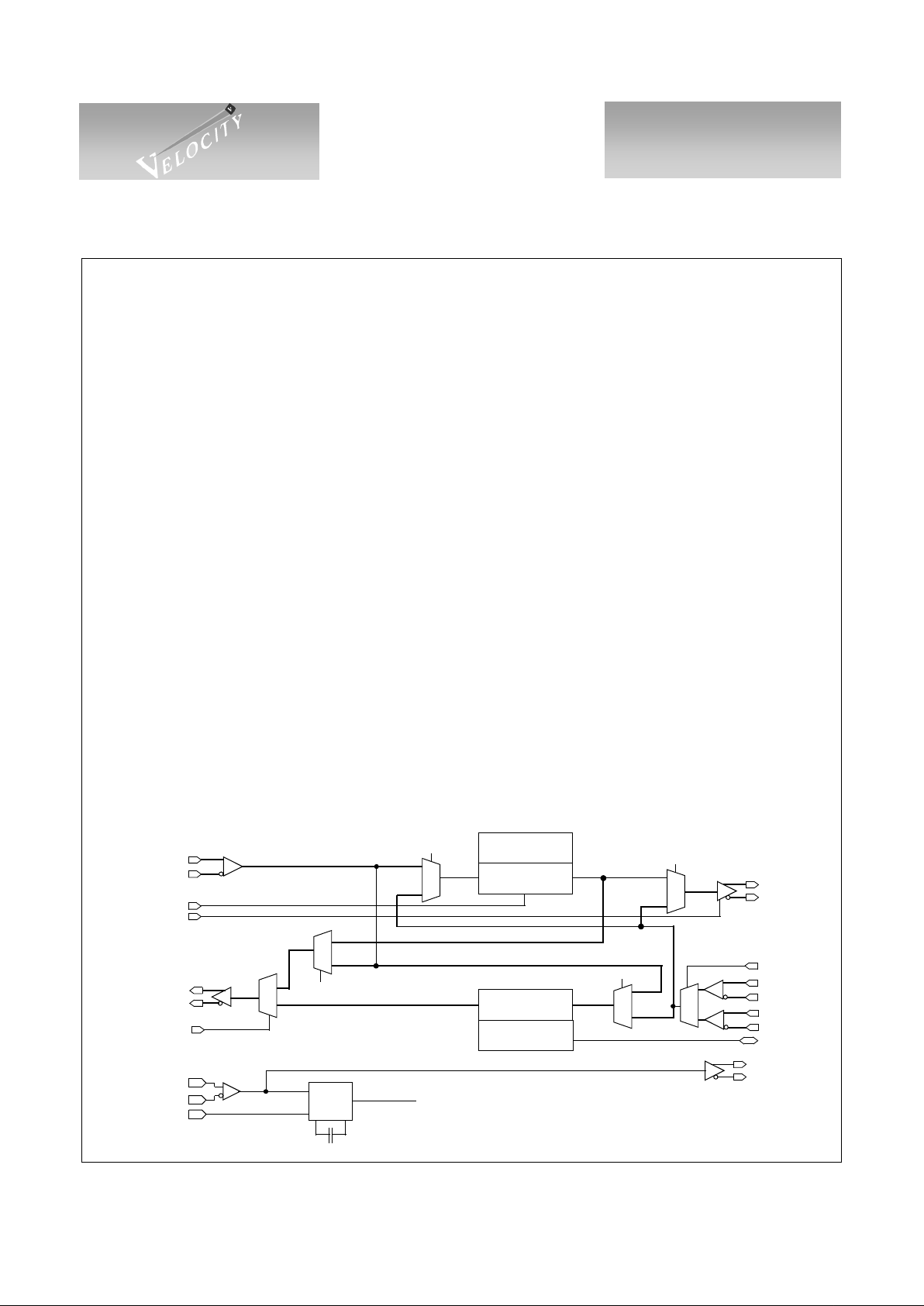
VSC7130 Block Diagram
• Used in Switches, Hubs, GBICs, MIAs and JBODs
• ANSI T11 Fibre Channel Compliant at 1.0625Gb/s
• IEEE 802.3z Gigabit Ethernet Compliant at 1.25Gb/s
• Dual Clock and Data Recovery Units Configurabl e as
Repeaters or Retimers
• Two-Wire Serial Communications Port for Control
and Status
• Combined Analog/Digital Signal Detect Units
• 1/10th or 1/20th Baud Rate TTL/PECL Reference Clock Input and PECL Output
• Bidirectional Analog/Digital Signal Detect
• 3.3V, 850mW Power Typical
• 64-pin, 10x10x1.0mm TQFP Package
• Cost Effective 0.35
µm CMOS Technology
SDET
SI+
SI-
TX+
TX-
SO+
SO-
RX1+
RX1-
CMU
REFI+
REFI-
HALF/FULL
1.0625 GHz
x10/x20
CAP0 CAP1
REFO+
REFO-
NOT SHOWN: Two-Wire Interface, test, modes and RXBIAS
CDR0
CDR1
SDU1
SDU0
MUX1
MUX2
MUX3
TXDIS
RX0+
RX0-
T/R
R1/0
0
1
BYP
1
0
0
1
MUX1SEL
MUX2SEL
0
1
53.125 or106 .25MHz
MUX4
0
1
MUX4SEL
MUX5
1
0
MUX5SEL
Clock Frequencies shown for Fibre Channel
Page 2
Data Sheet
VSC7130
Dual Repeater/Retimer
for Fibre Channel and Gigabit Ethernet
Page 2 G52297-0, Rev 4.0
04/02/01
© VITESSE SEMICONDUCTOR CORPORATION • 741 Ca ll e Pl an o • Camarillo, CA 93012
Tel: (800) VITESSE • FAX: (805) 987-5896 • Email: prodinfo@vitesse.com
Internet: www.vitesse.com
VITESSE
SEMICONDUCTOR CORPORATION
Applications
Several Fibre Channel and Gigabit Ethernet applications can use the VSC71 30. Configuration changes
between different applications are accomplished with mode pins and the Two-Wire Interface. SI+/- and SO+/-
are normally connected to the duplex i nterface from the sys tem while TX+/- and RX0+/- or RX1+/- are connected to the external link through a connector or optical transceiver. Redundant receive inputs are provided in
order to optimize layouts with copper connectors or optical modules. CDR0 improves the s ignal quality of SI
and retransmits the data on TX. CDR1 improves signal quality of RX0 or RX1 and retransmits recovered data
to SO.
In this document, the term “Repeater” will be used for a clock and data recovery function (CDR) where the
recovered serial data is retransmitted synchronously to the recovered clock. Unlike standard PLL-based CDRs,
this circuit is al l -di gi tal wh ich r esul t s i n good jitter toler anc e, excellent jitter t ransf er a nd low latency in a cir cu it
which performs identically across process, voltage and temperature.
The term “Retimer” is used for a CDR which retransmits the recovered serial data synchronously to the
local reference clock. This complex CDR function eliminates jit te r transfer at th e expe nse of l ate ncy. Due to the
potential mismatch between the baud rate of the incoming data and the local reference clock (i.e. +/-100ppm),
an add/drop elasticity buffer is neede d to insert/delete O rdered Sets to match th is rate difference. The data
which is added/dropped must meet Fibre Channel protocol specifications. By eliminating jitter transfer, standards compliance is ensured. The retimer function is not available for Gigabit Ethernet.
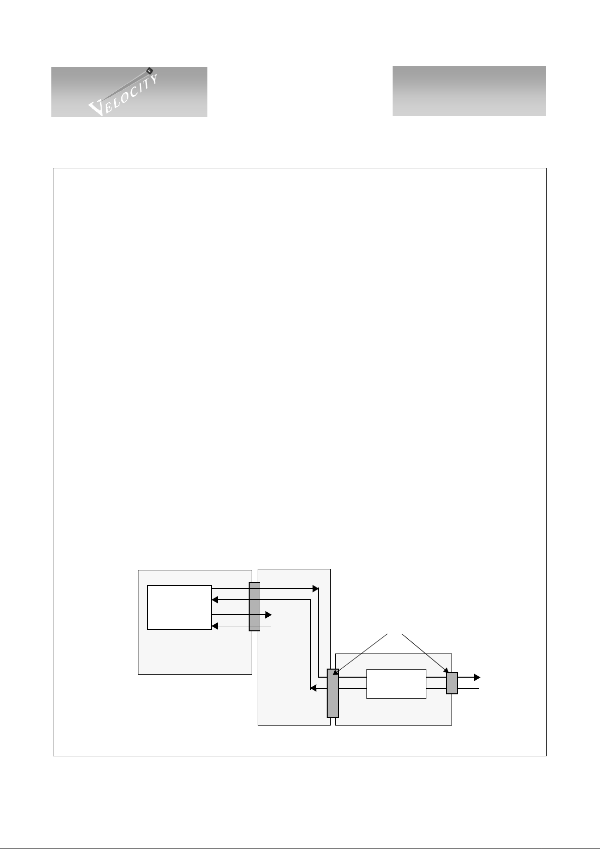
Multi-Node Switch
One application for the VSC7130 is in high port- cou nt Fibre C hanne l and Gigabi t Eth ernet systems such as
switches. Figure 1 shows a switch with a CMOS protocol ASIC with integrated Serializer/Deserializers located
on the Switch Fabric card. Serial data from the protocol ASIC passes through multiple connectors and long
traces on the PCB before reaching the connector. Without the VSC7130, the signal quality at the connectors
would result in poor system performance. However, by using the VSC7130, signal quality is improved to meet
the specifications of Fibre Channel and Gigabit Ethernet at the system interface connectors.
Figure 1: Fibre Channel or Gigabit Ethernet Switch
Protocol ASIC
Switch Fabric Card
Line Card
Connectors
VSC7130
Backplane
Port 1
CDR0>
<CDR1
Port N
Page 3
Data Sheet
VSC7130
Dual Repeater/Retimer
for Fibre Channel and Gigabit Ethernet
G52297-0, Rev 4.0 Page 3
04/02/01
© VITESSE SEMICONDUCTOR CORPORATION • 741 Calle Plano • Camarillo, CA 93012
Tel: (800) VITESSE • FAX: (805) 987-5896 • Email: prodinfo@vitesse.com
Internet: www.vitesse.com
VITESSE
SEMICONDUCTOR CORPORATION
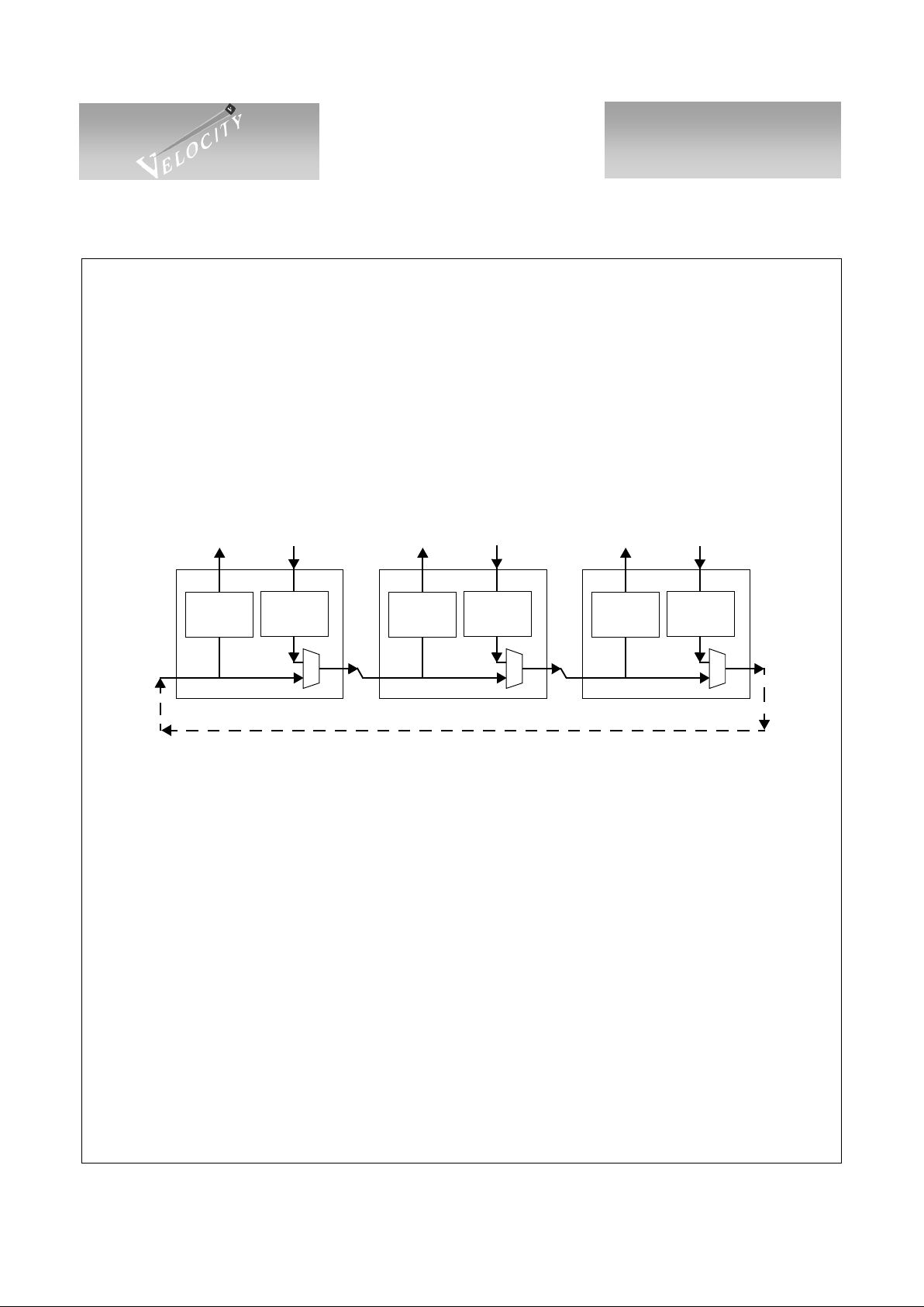
Fibre Channel Hub
The VSC7130 may be used as a single node in a Fibr e Channel A rbitrated Loop Hub. In this application,
incoming data on RX goes through a rep eat er (CDR1) which red uces ji tter. The data is then output on SO to the
next hub node. Incoming data from the previous hub node on SI goes through CDR0 which is configured as a
retimer to eliminate any ji tter ge nera ted inside the Hub . A by pass mu ltip lex er (M UX3) i s us ed t o by pass n odes
which do not have active devi ces connect ed. The si gnal d etection ci rcuitry id entifies v alid dat a at RX in order to
control the configuration of MUX3. The BYP pin may be connected vi a an invert er to SDET, BYP may be con-
trolled externally or MUX3 may be controlled via the Two-Wire Interface.
Access to internal registers through the Two-Wire Interfaces allows numerous features requires by sophi st icated managed Hubs such as Ordered Set Recognition, Ordered Set Generation and simple traffic monitoring.
Figure 2: Fibre Channel Arbitrated Loop Hub
Optical/Electrical Transceiver (GBIC)
As a dual repeater, the VSC7130 may provi de the func tions requ ired on an Op tical/El ectrical t ranscei ver
such as an Optical or an a active copper Gigabit Interface Converter (GBIC). In this application, outgoing data
from a system goes through CDR0 which can be configured as either a repeater or a retimer. Incoming data
passing through repeater CDR1 is transferred to the system. This function implements the critical circuits in an
active GBIC including RX_LOS.
CDR0
Retimer
CDR1
Repeater
SI
SO
RX
TX
CDR0
Retimer
CDR1
Repeater
SI
SO
RX
TX
CDR0
Retimer
CDR1
Repeater
SI
SO
RX
TX
Internal Loop
External
Device
External
Device
External
Device
Node N-1
Node N+1
MUX3 MUX3MUX3
Node N
Page 4
Data Sheet
VSC7130
Dual Repeater/Retimer
for Fibre Channel and Gigabit Ethernet
Page 4 G52297-0, Rev 4.0
04/02/01
© VITESSE SEMICONDUCTOR CORPORATION • 741 Ca ll e Pl an o • Camarillo, CA 93012
Tel: (800) VITESSE • FAX: (805) 987-5896 • Email: prodinfo@vitesse.com
Internet: www.vitesse.com
VITESSE
SEMICONDUCTOR CORPORATION
Figure 3: Active Copper GBIC Module
Functionality
Note this datasheet does not co mpletely describe the V SC7130. A c ompanion docume nt, the VSC7130
User’s Manual describes additional applications issues and goes into great depth regarding the Two-Wire Inter-
face and internal register operation.
Notation
All I/O pin names are in bold. All register bit nam es are italicized. Differential signals can be identifi ed
individually, e.g., I0+ and I0-, or together, e.g., I0. Signals and circuits w hich are r epeated a re generica lly
named using an ‘x’ to denote “any channel”, e.g., TXx for any Transmit pins. All registers are identified by
underlining, e.g., CDRxC
and the address for each referenced register will be listed immediately following the
register name (i.e. CDRxC-20h
).
Clock Multiplier Unit and Reference Clock
A reference clock is needed for the c lock multip lier un it (C MU) in o rder to gener ate th e intern al bau d rate
clock. The VSC7130 is used for both Fibre Channel (1.0625Gb /s) and Gigabit Ethernet (1.25Gb/s) appl icatio ns.
The HALF/FUL L signal indicates whether the reference clock is 1/20
th
of the baud rate (HIGH) or 1/10th of
the baud rate (LOW). Table 1 indicates the valid combinations of the HALF/FULL signal and reference clock
frequency. Combinations not listed in the table will result in abnormal functionality.
Table 1: Reference Clock Frequency Selection
HALF / FULL Pin Frequency (MHz) Application
HIGH 53.125 Fibre Channel @ 1.06 25Gb/s
LOW 106.25 Fibre Channel @ 1.0625Gb/s
HIGH 62.5 Gigabit Ethernet @ 1.25Gb/s
LOW 125.0 Gigabit Ethernet @ 1.25 Gb/s
All Other Combinations Not Allowed.
CDR1
Repeater
SO+
SO-
RX+
RX-
CDR0
Repeater
+TX_DAT
-TX_DAT
TX_DISABLE
TX_FAULT
+RX_DAT
-RX_DAT
RX_LOS
MOD_DEF0
MOD_DEF1
MOD_DEF2
SI+
SI-
TX+
TX-
GBIC CONNECTOR, 20-PIN SCA-2
DB-9 or HSSDC
VSC7130
SDET
SERIAL
EEPROM
OSC
TXDIS
RX+
TX+
RX-
TX-
Page 5
Data Sheet
VSC7130
Dual Repeater/Retimer
for Fibre Channel and Gigabit Ethernet
G52297-0, Rev 4.0 Page 5
04/02/01
© VITESSE SEMICONDUCTOR CORPORATION • 741 Calle Plano • Camarillo, CA 93012
Tel: (800) VITESSE • FAX: (805) 987-5896 • Email: prodinfo@vitesse.com
Internet: www.vitesse.com
VITESSE
SEMICONDUCTOR CORPORATION
Implementing reference clock distribution in multi-node systems can be difficult and expensive if optimal
signal quality is to be achieved. In order to reduce this bur den, the VSC7130 has a flexible reference input
buffer which can be either single- ended TTL, or differential PECL. If si ngl e-ended TTL, REFI+ should be connected to the clock source and REFI- should be left unconnected. REFI- is biased to V
DD
/2 for TTL thresh-
olds. If a PECL source is used, connect the positive side to REFI+ and the negative side to REFI-. In order to
provide the reference clock to multiple devices, a reference clock output, REFO+/-, is provided which is just a
PECL buffered version of REFI+/-. In this way, multiple VSC7130s m ay be daisy chained together with the
REFO driving the REFI of the next device. When REFO is driving REFI, a 100
Ω resistor should be con-
nected between REFI+ and REFI-.
The reference clock is used by the clock multiplier unit (CMU) in order to gener ate the internal baud rate
clock. In order to maximize signal quality of the TX and SO outputs, the REFI input should be of the highest
quality possible with sharp edges and l ow jitt er. Duty cycle distortion is not very important sinc e only the rising
edge of REFI is used. The CMU is a high perfor mance an alog PLL w hich multiplies the reference clock frequency by 20 or 10 depending on HALF/FULL.
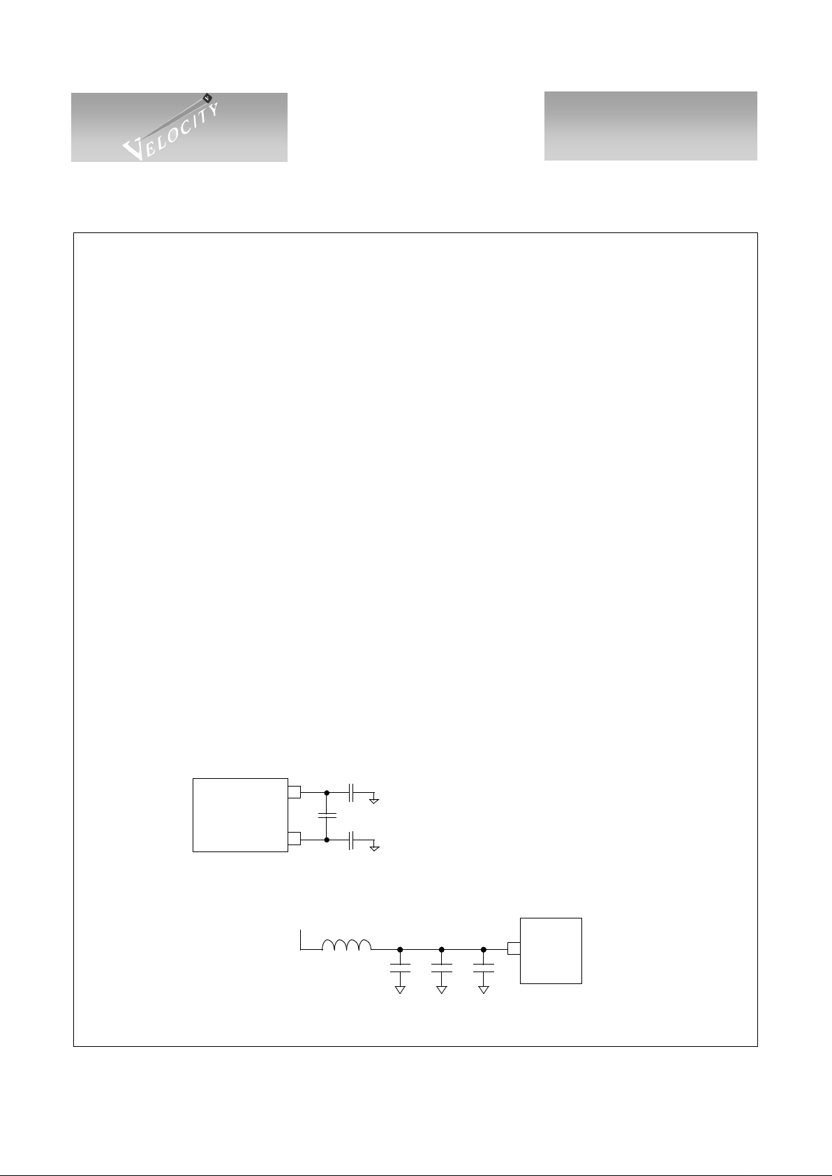
The on-chip PLL uses a single external 0.1µF capacitor, connected between CAP0 and CAP1, to control
the Loop Filter. This capacitor should be a multilayer ceramic dielectric, or better, with at least a 5V working
voltage rating and a good temp erat ure coefficient, i.e. NPO is preferred but X7R is acceptable. The se capacitors
are used to minimize the impact of common mode noise on the CMU , especially power supply noise. Higher
value capacitors provide better robust ness in syste ms. NPO i s preferred becau se i f an X7R capacitor is used, the
power supply noise sensitivity will vary with temperature. For best noise immunity, the designer may use a
three capacitor circuit with one differential capacitor between CAP0 and CAP1, C1, a capacitor from CAP0 to
ground, C2, and a capacitor from CAP1 to ground, C3. Lar g er values are be tter but 0.1µF i s adequat e. However,
if the designer cannot use a three capacitor circuit , a si ngl e differential capacitor, C1, is adequate. These components should be isolated from noisy traces. Figure 4 is the recommended Loop filtering scheme.
Separate power (VDDA) and ground (VSSA) are provided in order to allow a separately filtered power
supply to reduce noise. Figure 5 is the recommended VDDA filtering scheme.
Figure 4: Loop Filter Capacitors (Recommended Circuit)
Figure 5: VDDA Filtering (Recommended Circuit)
CAP0
CAP1
C1
C2
C3
VSC7130
C1=C2=C3= >0.1µF
MultiLayer Ceramic
Surface Mount
NPO (Preferred) or X7R
5V Working Voltage Rating
VDDA
VDD
C1=10-33µF
C3C2C1
L1
C2=0.1µF
C3=0.01µF-0.001µF
L1=Ferrite bead with
high impedance at high frequencies
and some DC resistance (0.5
Ω)
VSSA
VSC7130
Page 6

Data Sheet
VSC7130
Dual Repeater/Retimer
for Fibre Channel and Gigabit Ethernet
Page 6 G52297-0, Rev 4.0
04/02/01
© VITESSE SEMICONDUCTOR CORPORATION • 741 Ca ll e Pl an o • Camarillo, CA 93012
Tel: (800) VITESSE • FAX: (805) 987-5896 • Email: prodinfo@vitesse.com
Internet: www.vitesse.com
VITESSE
SEMICONDUCTOR CORPORATION
Input and Output Buffers, Analog Signal Detection, Cable Equalization
The RX0+/-, RX1+/- and SI+/- differential i nputs are h igh performa nce inpu t buffers which amplify the
incoming signal. Furthermore, a cable equalization circuit is included in the input buffer which accentuates
high frequency signals in order to co mpensate for the high frequenc y loss found in copper cable s and traces .
This cable equalization circuit enhances the ability of the VSC7130 to reliably receive serial inputs which have
been degraded with jitter. The RX 1+/- input buffer also includes an analog signal detection circuit which has
adjustable thresholds set by the external RXBIAS pin (see Figure 9). The output of this signal is processed further in the Signal Detection circuitry described elsewhere, as well as selectable threshold levels which are
selected with the RXBIAS input.
If the Two-Wire Interface is not used, R1/0 directly controls the RX0 and RX1 input buffers and Cable
Equalization is enab led in SI, RX0 and RX1. If the Two-Wi re Interface is used, microcontroller control allows
enabling or disabling of the cable equalization circuit.
Please refer to the VSC7130 User’s Manual for a more complete description of the input and output buffer
controls and cable equalization controls.
High-Speed I/O Termination Schemes
The high-speed I/O lines for the VSC7130 require the standard Vitesse 1Gb/s CMOS device termination
schemes. Plea se re fe r to the Termination for 1Gb/s CMOS Devices Applicatio n Note (AN-54) fo r VSC7130 RX
and TX termination schemes. When using the REFI+/- and REFO+/- pins on the VSC7130 in daisy-chained
clock applications, specific termination must be implemented. If the REFO+/- pins of one VSC7130 are to be
routed to the REFI+/- pins of a second VSC7130, 50
Ω single-ended (100Ω differential) traces should be used.
AC coupling caps should be placed between the two VSC7130s. Additionally, a 100
Ω 1% termination resistor
should be place between the REFI+ and REFI- lines of the second VSC7130. This termination resistor should
be located as close to the REFI+/- pins as possible. Figure 6 shows the recommended termination and compo-
nents when using the VSC7130’s REFI and REFO.
Figure 6: REFI and REFO Recommended Termination
VSC7130 #1
REFI+
REFI-
REFO+
REFO-
Oscillator
(TTL)
53.125 or 106.25MHz
X
VSC7130 #2
REFI+
REFI-
REFO+
REFO-
22
Ω
100
Ω
1%
0.01µF
0.01
µ
F
50
Ω
1%
50
Ω
1%
0.01µF
0.01µF
Page 7
Data Sheet
VSC7130
Dual Repeater/Retimer
for Fibre Channel and Gigabit Ethernet
G52297-0, Rev 4.0 Page 7
04/02/01
© VITESSE SEMICONDUCTOR CORPORATION • 741 Calle Plano • Camarillo, CA 93012
Tel: (800) VITESSE • FAX: (805) 987-5896 • Email: prodinfo@vitesse.com
Internet: www.vitesse.com
VITESSE
SEMICONDUCTOR CORPORATION
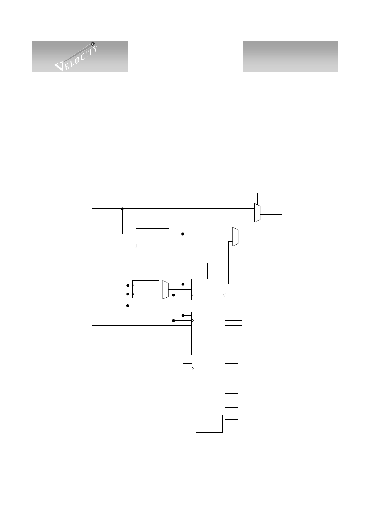
Clock and Data Recovery (CDR)
Two Clock and Data Recovery Units (CDR) are included in the VSC713 0 in order to improve signal qual ity of
serial data by amplification and jitter attenuation. Figure 7 shows a block diagram of each CDR with its corresponding Signal Detect Unit (SDU). Table 2 shows how each CDR may be configured as either a repeater or a
retimer using the MODE0, MODE1 and T/R pins or via the Two-Wire Interface by programming the MODEDIS,
T/RDIS and ITRx register bits.
Figure 7: CDRx/SDUx Block Diagram
OSGxSEL
Q
CLKO
D
REPEATERx
OSGENxA
OSGENxB
0
1
Serial In
Serial Out
RLLDISx
K28DISx
RLLx
K28x
ASDx
ASDDISx
KWINDx(5:0)
PSDx
QD
RETIMERx
D
SDUx
SDx
Analog Signal Detect In
Baud Rate Clock
D
HUB
IDLEx
Support
(from CMU)
BYPx
OSREC0A
OSREC0B
ARBx
OPENx
CLSx
OSRxA
OSRxB
LIPF7,F7x
LIPF8,F7X
LIPF7,Xx
LIPF8,Xx
LIPYXx
ADDx
DROPx
OVERx
(from input buffer)
UNDERx
LIPFFx
NLIPF8x
1
0
1
0
SELRTx
(derived from
MODE[1:0], T/R
,
MODEDIS, T/RDIS and
and ITRx)
OSGENx
Page 8

Data Sheet
VSC7130
Dual Repeater/Retimer
for Fibre Channel and Gigabit Ethernet
Page 8 G52297-0, Rev 4.0
04/02/01
© VITESSE SEMICONDUCTOR CORPORATION • 741 Ca ll e Pl an o • Camarillo, CA 93012
Tel: (800) VITESSE • FAX: (805) 987-5896 • Email: prodinfo@vitesse.com
Internet: www.vitesse.com
VITESSE
SEMICONDUCTOR CORPORATION
T able 2: CDRx Repeater/Retimer Configuration
The SELRTx signal determines whether the repeater or retimer output is selected, as shown in Figure 4.
The MODEDIS register bit (CHIPCA
-01h, bit 7) and the T/RDIS register bit (CHIPCA-01h, bit 4) can be
used to disable the pin controls defined in Table 2 for selecting repeater or retimer mode for each CDR unit. For
CDR0, if the MODEDIS and T/RDIS bits are both set, the ITR0 register bit (CDR0C
-20h, bit 4) will control the
repeater/retimer selection. For CDR1, only the MODEDIS register bit needs to be set in order to use ITR1
(CDR1C
-28h, bit 4) to control the repeater/retimer selection. A HIGH in ITRx selects repeater mode, and a
LOW selects retimer mode.
Normally, the SI inp ut pa sses t hr oug h M UX1 to t he input of CDR0 whose ou tput is transmitted on TX+/- if
TXDIS is LOW. If TXDIS is HIGH, TX+ and TX- will be HIGH. Similarly, the RX input normally passes
through MUX2, CDR1 and MUX3 to the SO output.
Retimer Operation
NOTE: Retimer operation is only used for Fibre Channel data at 1.0625Gb/ s. Do not use Retimer mode
unless the incoming data is Fibre Channel or follows the Ordered Set structure defined by Fibre Channel. Failure to do so will result in data corruption.
When CDRx is configured as a Retimer, recovered data is resynchronized to an internally generated baud
rate clock derived from the REFI. This prevents jitter at the inputs from transferring to the outputs. However,
incoming data is not necessarily at the same frequency as the internal baud rate clock, so special Fibre Channel
Ordered Sets, called Fill Words, are added or dropped from the data stream in order to accommodate this speed
difference. The rules for adding and dropping Fill Words are delineated in documents generated by the T11
committee: FC-PH, FC-PH2, FC-PH3, FC-AL, FC-AL2 and FC-AL3. The VSC7130 is compliant with these
rules.
A detailed block diagram of the Retimer is shown in Figure 8. Incoming data goes into a CRU where the
data is recovered and resampled. Recovered data and recovered clock are sent to the Add/Drop FIFO where the
data is stored using the recovered clock. Data is removed from the Add/Drop FIFO and resynchronized by the
Retransmitting Flip-Flop using the internally generated baud rate clock derived from REFI. The output of the
Flip-Flop is recovered serial data which is synchronous to the low-jitter baud rate clock and complies with all
jitter specifications for Fibre Channel.
MODE1 Pin MODE0 Pin T/R Pin CDR1 CDR0
00
0 Repeater (SELRT1=1) Repeater (SELRT0=1)
1 Repeater (SELRT1=1) Retimer (SELRT0=0)
01
0 Repeater (SELRT1=1) Repeater (SELRT0=1)
1 Repeater (SELRT1=1) Retimer (SELRT0=0)
10
n/a Bypass Bypass and power down
n/a Bypass Bypass and power down
11
0 Retimer (SELRT1=0) Repeater (SELRT0=1)
1 Retimer (SELRT1=0) Retimer (SELRT0=0)
Page 9

Data Sheet
VSC7130
Dual Repeater/Retimer
for Fibre Channel and Gigabit Ethernet
G52297-0, Rev 4.0 Page 9
04/02/01
© VITESSE SEMICONDUCTOR CORPORATION • 741 Calle Plano • Camarillo, CA 93012
Tel: (800) VITESSE • FAX: (805) 987-5896 • Email: prodinfo@vitesse.com
Internet: www.vitesse.com
VITESSE
SEMICONDUCTOR CORPORATION
Figure 8: Retimer Block Diagram
The internally generated baud rate clock (nominally 1. 0625GHz) is us ed by the Retimer for sever al functions. First, it provides the timing reference for the CRU. Second, it clocks data out of the FIFO. Third, it
retimes the retransmitted output data. The quality of the baud rate clock will impact the jitter tolerance of the
Clock Recovery Unit and the jitter generation of the Retransmitter Flip-Flop. The signal quality of the internally
generated baud rate clock i s di rect l y r el ated to jitter on REFI a nd po we r su pply noise. The user is encouraged to
minimize both REFI jitter and power supply noise in orde r to maximize jitter tolerance a t the input and minimize jitter generation at the output.
In the Add/Drop FIFO, a phase detector monitors the phase difference between the recovered clock and the
internally generated baud rate cl ock to dete rmine when to add or dr op Fill Words. Fill W o rds can only be added/
dropped between packets following the rules delineated by the Fibre Channel Specifications mentioned previously.
The retimer has two outputs indicating whether it is adding (ADDx) or dropping (DROPx) ordered sets
from the serial stream in order to perform rate matching between the incoming serial data and the local reference clock. The retimer also has an output (OVERx) indicating that an overrun condition has occurred when an
order set which needed to be dropped was not able to be dropped. Similarly, underrun errors are reported when
a Fill Word which needed to be added was not able to be added.
Please refer to the VSC7130 User’s Ma nual for more information regarding retimer operation and associ-
ated register controls.
Signal Detection
Associated with each CDR is a Signal Detect Unit (SDU) which is used to determine if a valid Fibre Channel signal is present at the CDR. Each SDU employs three independent checks to q ualify the signal as valid:
K28.5- primitive detection, Run-Length-Limit (RLL) error detection and K28.5- density checking. In addition,
when the RX1 input pair is selected for input (instead of RX0), SDU1 also uses the Analog Signal Detect
(ASD) circuit associated with the RX1 input pair as an additional signal detect qualification.
Signal Detect assertions and deassert ions are trigger ed by di ff erent co nditi ons observed by the VSC 7130 on
the incoming serial data signal. Signal Detect assertions are triggered only when two consecutive valid Fibre
Clock
Q
CLKO
D
ADD/DROP
Q
CLK
D
CLKI
Retransmit
QD
CLK
INPUT
DATA
To RTMRxC Register
1.0625GHz Internal Baud Rate Clock
CLKI
OUTPUT
DATA
Flip-Flop
FIFO
UNDERx
OVERx
ADDx
DROPx
Recovery
Unit
Page 10

Data Sheet
VSC7130
Dual Repeater/Retimer
for Fibre Channel and Gigabit Ethernet
Page 10 G52297-0, Rev 4.0
04/02/01
© VITESSE SEMICONDUCTOR CORPORATION • 741 Ca ll e Pl an o • Camarillo, CA 93012
Tel: (800) VITESSE • FAX: (805) 987-5896 • Email: prodinfo@vitesse.com
Internet: www.vitesse.com
VITESSE
SEMICONDUCTOR CORPORATION
Channel primitives containing K28.5- characters are received. Once Signal Detect is asserted, there are several
conditions which can result in t he deasser t i on of Si gnal Detect: (1) An RLL error (a viol at io n of 8B/10B coding
rules in which there are mor e than five cons ecutive zero s or ones in the data stream), (2) no K2 8.5- charac ter
seen for one density window time (defaults to apx. 77 microseconds, but can be modified using the Two-Wire
Interface to write to the KWINDx
-25h/2Dh register), or (3) an invalid signal level detected by the Analog Sig-
nal Detect circuit (only applies to SDU1 when the RX1 input is selected).
The Analog Signal Detect circuit is used to ensure that the signal am plitude presented to the RX1 input pair
is high enough to be considered va lid. Analog tra nsition detection is pe rformed on the input to verify that the
signal swings are of adequate amplitude. The RX1+/- input buffer conta ins a differential voltage c omparato r
which has adjustable thresholds set by the external RXBIAS pin (see Figure 9). If the Two-Wire Interface is
being used, the Analog Signal Detect check for SDU1 can also be disabled by setting the ASDDIS1 register bi t
(SDU1C
-29h, bit).
Figure 9 shows an approximation to the Analog Signal Detect thresholds which can be obtained with biasing resistors or another voltage reference source to the RXBIAS pin.
Figure 9: VSC7130 RXBIAS Equations and Graph
1. From the graph find the op timal SDET trip threshold for yo ur system. It is recommended that
the rising edge of the graph be used unless pulli ng RXBIAS to ground via a 1kΩ resistor.
2. From the SDET threshold, determine the voltage level for RXBIAS fr om V
RXBIAS
/VDD. In
most systems, VDD is assumed to be 3.3V and V
RXBIAS
is the voltage seen at the RXBIAS pin.
3. Use the equations to determine the resistance values for R1 and R2. The use of 1% resistors for
R1 and R2 is recommended. Other regulated voltage sources may be used as long as the
minimal current is provid ed.
100
200
300
400
500
600
0.00 0.20 0.40 0.60 0.80 1.00
V
RXBIAS
/VDD
SDET Threshold Voltage
(mV, pk-pk differential)
R1
R2
RXBIAS
VSC7130
RXBIAS
Pin 46
3.3V
R1 x R2
R1 + R2
1k
Ω
R1
<
~
<
_
3.3V - V
RXBIAS
150uA
R2
<
_
V
RXBIAS
50uA
Page 11

Data Sheet
VSC7130
Dual Repeater/Retimer
for Fibre Channel and Gigabit Ethernet
G52297-0, Rev 4.0 Page 11
04/02/01
© VITESSE SEMICONDUCTOR CORPORATION • 741 Calle Plano • Camarillo, CA 93012
Tel: (800) VITESSE • FAX: (805) 987-5896 • Email: prodinfo@vitesse.com
Internet: www.vitesse.com
VITESSE
SEMICONDUCTOR CORPORATION
Hub Support
Several functions are provided in the CD Rx/SDUx c ircuitry to support FC-AL H ubs. Two programmable
40-bit registers are available to ge nerat e dat a on TX or SO, allowing simple 40-bit patterns to be generated eas-
ily. Monitoring of the serial data out of the repeater provides the user with information concerning data content
of packets as they are received. Many FC-AL ordered sets are detected (all ARBs, IDLE, all LIPs, all CLS and
all OPENs). Furthermore, two 40-bit registers/comparators are provided to allow the user to identify when user
programmable patterns occur in the data. One use of these would be to monitor for the presence of ordered sets
defined after release of this product.
Please refer to the VSC7130 User ’s Manual for a more complete description of the ordered set generation
and recognition capabilities and associated register controls.
Performance Monitoring
In order to deter mine the rela tive tr affic on the li nk, a 32- bit c oun ter is pr ovi ded wh ich inc rem en ts on each
occurrence of an ARB ordered set or an IDLE ordered set. By reading this counter periodically, the relative traffic on the link can be calculated.
Please refer to t he VSC7130 User’s Manual for a more complete description of the performance monitoring
capabilities and associated register controls.
Power-On-Reset
The VSC7130 has an internal Power -On-Re set c ircuit to prov id e appro xima tely o ne mill is econ d delay after
power up during which all Two-Wire accessible registers are reset. An alternate method for resetting the device
is available. If TEST0 and A4 are LOW, the device is reset. Connect an active LOW Reset signal to TEST0 and
A4 if it would be HIGH during normal operation. When the reset input is LOW, the alternative reset method is
activated. When the reset input is HIGH, TEST0 and A4 assume their normal value.
Two-Wire Interface
An industry-standard Two-Wire Interface is provided to allow user access to internal con trol and stat us. Use
of the interface is optional. SCL is the serial interface clock running at up to 400kHz when used with read ily
available microcontrollers. SDA is a bidirectional data signal. A4 and A3 selects the group address of the device
while A2-A0 set the address. TWI and TWO are used to seri ally configure the addres s of da isy-ch ained de vices
in order to accommodate large numbers of devices on each Two-Wire Interface link. INT# is an open drain output used to signal an interruptible event to the microcontroller.
Please refer to the VSC7130 User’s Manual for a more complete description of this interface, includi ng tim-
ing diagrams.
Proprietary Interface
If higher perf ormanc e than 40 0kHz is require d, a prop rietary m ode ma y be used . In this mode, the SCL
clock can operate at a maximum speed of 6.25MHz. Due to the speed of this link, significant electrical limitations may be placed on the l ink which wil l restri ct trace lengt hs, the n umber of da isy-chained de vices and t he
use of multiple masters.
Page 12

Data Sheet
VSC7130
Dual Repeater/Retimer
for Fibre Channel and Gigabit Ethernet
Page 12 G52297-0, Rev 4.0
04/02/01
© VITESSE SEMICONDUCTOR CORPORATION • 741 Ca ll e Pl an o • Camarillo, CA 93012
Tel: (800) VITESSE • FAX: (805) 987-5896 • Email: prodinfo@vitesse.com
Internet: www.vitesse.com
VITESSE
SEMICONDUCTOR CORPORATION
The Verilog code for the Master Controller in proprietary mode will be made available to customers in
order to ensure compatibility. This Master Controller core is designed to use either a 25MHz or a 50MHz clock
to generate a 6.25MHz SCL clock frequency with a 25% high, 75% low duty cycle (1 clock high, 3 clocks low
at 25MHz). Slower clock frequencies are also allowable.
When using the Proprietary High-Speed mode o f the Two-Wire Interface, all other interface fu nctio nality i s
identical to the standard Two-Wire Interface with the exception that the interface timing has changed.
Interrupt Circuitry
Interrupts are avai lable only when the Two-Wire Interface is used, other wise INT# will be disabled. The
INT# output is open-drain so an external pul l-up re sistor is ne eded to al low the outpu t to achi eve a valid TT L or
CMOS HIGH level. Multiple INT# outputs can be wire ORed together. INT# is a glitchless signal which i s synchronized to divide-by-32 REFO clock. The output of the interrupt controller prior to the output buffer is readable in the INTOUT register bit, bit 2 of the CHIPS
-00h register.
The VSC7130 is capable of managing sever al dif fer ent kinds of interna l inter rupt condi tions. Each interr upt
source can be enabled independently using the registers accessible via the Two-Wire Interface. When an
enabled interrupt event occurs, the open-drain INT# output will be asserted LOW and will stay LOW until the
interrupt is cleared. The register address corresponding to the highest priority pending interrupt can be read
from ISR
-F8h. This provides a relatively fast means for determining the source of the interrupt with a single
register read operation.
Please refer to the VSC7130 User’s Manual for a more co mplete de script ion of the interrup t controll er and
its associated register controls.
Table 3: Interrupt Status Register Addresses, Priorities and Sources
Figure 10: Block Diagram of Interrupt Output
Address
(Hex)
Priority Label Function
22 1 (Highest) SDU0S SDU0 Status Register: SDR0 (7), SDF0 (6), ASD0 (2), RLL0 (1), K280 (0)
2A 2 SDU1S
SDU1 Status Register: SDR1 (7), SDF1 (6), ASD1 (2), RLL1 (1), K281 (0)
23 3 RTMR0C
Retimer0 Configuration Register: UNDER0 (6), OVER0 (4), ADD0 (2), DROP0 (0)
2B 4 RTMR1C Retimer1 Configuration Register: UNDER1 (6), OVER1 (4), ADD1 (2), DROP1 (0)
6C 5 MATCHA0 Ordered Set Match Register A for CDR0: All Bits except RES (1)
6D 6 MATCHB0
Ordered Set Match Register B for CDR0: All Bits except RES (6)
7C 7 MATCHA1 Ordered Set Match Register A for CDR1: All Bits except RES (1)
7D 8 MATCHB1 Ordered Set Match Register B for CDR1: All Bits except RES (6)
F4 9 ( Lowest) TEST4
Test Register 4: TESTINT (4) for diagnostics
INT#
INTOUT
Interrupt
Controller
(CHIPS-00h, bit 2)
VDD
Shared by Other
Devices
Page 13

Data Sheet
VSC7130
Dual Repeater/Retimer
for Fibre Channel and Gigabit Ethernet
G52297-0, Rev 4.0 Page 13
04/02/01
© VITESSE SEMICONDUCTOR CORPORATION • 741 Calle Plano • Camarillo, CA 93012
Tel: (800) VITESSE • FAX: (805) 987-5896 • Email: prodinfo@vitesse.com
Internet: www.vitesse.com
VITESSE
SEMICONDUCTOR CORPORATION
Programmable Registers
A list of the programmable registers accessible by the Two-Wire Interface is shown in Table 4. This list
includes the address of the regi ster, whether it is Readable and/or Writable, i f i t is a so urce of interrupts, the register’s name and function.
Table 4: Programmable Registers
Address
(Hex)
Read/
W rite
(or Clear)
Interrupt
Source
Label Function
CONFIGURATION/STATUS REGISTERS
00 R N CHIPS Chip Status Register
01 R/W N CHIPCA Chip Configuration Register A
02 R/W N CHIPCB
Chip Configuration Register B
03 R/W N CHIPCC Chip Configuration Register C
CDR0/CDR1
20/28 R/W N CDRxC
CDRx Configuration Register
21/29 R/W N SDUxC SDUx Configuration Register
22/2A R/C Y SDUxS
SDUx Status Register
23/2B R/W/C Y RTMRxC
Retimer0 Configuration Register
25/2D R/W N KWINDx
K28.5- Signal Detect Density Window Register for SDUx
60/70 R/W N OSGENxA0
Ordered Set Generator A, Bits 39-32 for CDRx
61/71 R/W N OSGENxA1 Ordered Set Generator A, Bits 31-24 for CDRx
62/72 R/W N OSGENxA2
Ordered Set Generator A, Bits 23-16 for CDRx
63/73 R/W N OSGENxA3
Ordered Set Generator A, Bits 15-8 for CDRx
64/74 R/W N OSGENxA4 Ordered Set Generator A, Bits 7-0 for CDRx
65/75 R/W N OSGENxB0
Ordered Set Generator B, Bits 39-32 for CDRx
66/76 R/W N OSGENxB1 Ordered Set Generator B, Bits 31-24 for CDRx
67/77 R/W N OSGENxB2 Ordered Set Generator B, Bits 23-16 for CDRx
68/78 R/W N OSGENxB3
Ordered Set Generator B, Bits 15-8 or CDRx
69/79 R/W N OSGENxB4 Ordered Set Generator B, Bits 7-0 for CDRx
6C/7C R/C Y MATCHAx Match Register A for CDRx
6D/7D R/C Y MATCHBx
Match Register B for CDRx
6E/7E R/W N MATIEAx Match Interrupt Enable Register A for CDRx
6F/7F R/W N MATIEBx Match Interrupt Enable Register B for CDRx
80/90 R/W N OSRECxA0
Ordered Set Recognition Register A, Bits 39-32 for CDRx
81/91 R/W N OSRECxA1 Ordered Set Recognition Register A, Bits 32-24 for CDRx
82/92 R/W N OSRECxA2 Ordered Set Recognition Register A, Bits 23-16 for CDRx
83/93 R/W N OSRECxA3
Ordered Set Recognition Register A, Bits 15-8 for CDRx
84/94 R/W N OSRECxA4 Ordered Set Recognition Register A, Bits 7-0 for CDRx
85/95 R/W N OSMASKxA0 Ordered Set Mask Register A, Bits 39-32 for CDRx
Page 14

Data Sheet
VSC7130
Dual Repeater/Retimer
for Fibre Channel and Gigabit Ethernet
Page 14 G52297-0, Rev 4.0
04/02/01
© VITESSE SEMICONDUCTOR CORPORATION • 741 Ca ll e Pl an o • Camarillo, CA 93012
Tel: (800) VITESSE • FAX: (805) 987-5896 • Email: prodinfo@vitesse.com
Internet: www.vitesse.com
VITESSE
SEMICONDUCTOR CORPORATION
NOTE: Please refer to the VSC7130 User’s Manual for a thorough description of each register and its function.
86/96 R/W N OSMASKxA1
Ordered Set Mask Register A, Bits 31-24 for CDRx
87/97 R/W N OSMASKxA2 Ordered Set Mask Register A, Bits 23-16 for CDRx
88/98 R/W N OSMASKxA3
Ordered Set Mask Register A, Bits 15-8 for CDRx
89/99 R/W N OSMASKxA4
Ordered Set Mask Register A, Bits 7-0 for CDRx
A0/B0 R/W N OSRECxB0
Ordered Set Recognition Register B, Bits 39-32 for CDRx
A1/B1 R/W N OSRECxB1 Ordered Set Recognition Register B, Bits 32-24 for CDRx
A2/B2 R/W N OSRECxB2
Ordered Set Recognition Register B, Bits 23-16 for CDRx
A3/B3 R/W N OSRECxB3 Ordered Set Recognition Register B, Bits 15-8 for CDRx
A4/B4 R/W N OSRECxB4 Ordered Set Recognition Register B, Bits 7-0 for CDRx
A5/B5 R/W N OSMASKxB0
Ordered Set Mask Register B, Bits 39-32 for CDRx
A6/B6 R/W N OSMASKxB1 Ordered Set Mask Register B, Bits 31-24 for CDRx
A7/B7 R/W N OSMASKxB2 Ordered Set Mask Register B, Bits 23-16 for CDRx
A8/B8 R/W N OSMASKxB3
Ordered Set Mask Register B, Bits 15-8 for CDRx
A9/B9 R/W N OSMASKxB4
Ordered Set Mask Register B, Bits 7-0 for CDRx
C0/D0 R/W N PCNT0x Performance Counter x, Bits 31-24 for CDRx
C1/D1 R/W N PCNT1x
Performance Counter x, Bits 23-16 for CDRx
C2/D2 R/W N PCNT2x
Performance Counter x, Bits 15-8 for CDRx
C3/D3 R/W N PCNT3x Performance Counter x, Bits 7-0 for CDRx
C4/D4 R/W N PCxCTL
Performance Counter x Control Register
MISCELLANEOUS REGISTERS
F0 - N TEST0
Test Register #0, For Factory Test Only, Do Not Access
F1 - N TEST1
Test Register #1, For Factory Test Only, Do Not Access
F2 - N TEST2
Test Register #2, For Factory Test Only, Do Not Access
F3 - N TEST3 Test Register #3, For Factory Test Only, Do Not Access
F4 R/W Y TEST4
Test Register #4, Soft Reset, TWOPOR & INT# Control
Register
F5 - N TEST5
Test Register #5, For Factory Test Only, Do Not Access
F6 - N TEST6
Test Register #6, For Factory Test Only, Do Not Access
F7 R/W N SADDR Soft ADDRess Register
F8 R/C N ISR Interrupt Status Register (Read, then write FFh to Clear)
FD R N MODEL1
Model Number Register (High Byte)
FE R N MODEL0 Model Number Register (Low Byte)
FF R N VER Version Regis ter
Address
(Hex)
Read/
W rite
(or Clear)
Interrupt
Source
Label Function
Page 15

Data Sheet
VSC7130
Dual Repeater/Retimer
for Fibre Channel and Gigabit Ethernet
G52297-0, Rev 4.0 Page 15
04/02/01
© VITESSE SEMICONDUCTOR CORPORATION • 741 Calle Plano • Camarillo, CA 93012
Tel: (800) VITESSE • FAX: (805) 987-5896 • Email: prodinfo@vitesse.com
Internet: www.vitesse.com
VITESSE
SEMICONDUCTOR CORPORATION
AC Characteristics (Over Recommended Operating Conditions)
Figure 11: AC Timing Diagrams
Ta ble 5: AC Characteristics (Over recommended operating conditions)
Parameters Description Min Typ Max Units Conditions
T
P
Latency from any Serial Input to any Serial
Output
0.25 — 8.75 ns No Retimer in path
T
S
Differential Output Rise/Fall time ——300 ps Between 20% and 80%
T
J(RPTR)
Total data output jitter
[Repeater Mode]
——192 ps
Jitter Generation at TX/SO
when driven by the CRU in
Repeater Mode. IE EE 802.3z
Clause 38.68
T
DJ(RPTR)
Serial data output deterministic jitter (p-p)
[Repeater Mode]
——80 ps
Jitter Generation at TX/SO
when driven by the CRU in
Repeater Mode. IE EE 802.3z
Clause 38.68
T
J(RTMR)
Total data output jitter [Retimer Mode] ——192 ps
Jitter Generation at TX/SO
when driven by the CRU in
Retimer Mode. IEEE 802.3z
Clause 38.68
T
DJ(RTMR)
Serial data output deterministic jitter (p-p)
[Retimer Mode]
——80 ps
Jitter Generation at TX/SO
when driven by the CRU in
Retimer Mode. IEEE 802.3z
Clause 38.68
T
JTOL
Jitter Tolerance at RX0/RX1/SI 0.24 ——UI
Minimum Eye Opening for
proper operation as de fined
in MJS 8.0.
T
T
REFI input rise/fall times ——1.5 ns
Between V
IL(MAX)
and
V
IH(MIN)
F REFI Frequency
105
52.5
—
126
63
MHz
HALF/FULL is LOW
HALF/FULL is HIGH
F
O
Frequency Offset between incoming data
and REFI.
-200 — +200 ppm
DC REFI Duty Cycle 30 70 % Measured at 1.5V
T
P
T
P
T
S
RX0+/-
TX+/-
REFI
T
T
T
T
T
H
T
L
T
V
IH(MIN)
V
IL(MAX)
80%
20%
T
S
RX1+/SI1+/-
SO+/-
Page 16

Data Sheet
VSC7130
Dual Repeater/Retimer
for Fibre Channel and Gigabit Ethernet
Page 16 G52297-0, Rev 4.0
04/02/01
© VITESSE SEMICONDUCTOR CORPORATION • 741 Ca ll e Pl an o • Camarillo, CA 93012
Tel: (800) VITESSE • FAX: (805) 987-5896 • Email: prodinfo@vitesse.com
Internet: www.vitesse.com
VITESSE
SEMICONDUCTOR CORPORATION
DC Characteristics (Over recommended operating conditions).
NOTE (1): Refer to Applicatio n Not e AN- 37 for differential measurement techniques.
Absolute Maximum Ratings
(1)
Power Supply Voltage (VDD).............................................................................................................-0.5V to +4V
PECL DC Input Voltage.........................................................................................................-0.5V to V
DD
+0.5V
TTL DC Input Voltage.......................................................................................................................-0.5V to 5.5V
DC Voltage Applied to TTL Outputs ...................................................................................-0.5V to V
DD
+ 0.5V
TTL Output Current ....................................................................................................................................±50mA
PECL Output Current..................................................................................................................................±50mA
Case Temperature Under Bias......................................................................................................-55°
C to +125
o
C
Storage Temperature....................................................................................................................-65°
C to + 150
o
C
Maximum Input ESD (Human Body Model)...............................................................................................1500V
NOTE:(1) CAUTION: Stresses listed under “Absolute Maximum Ratings” may be applied to devices one a t a time witho ut causing
permanent damage. Functionality at or above the values listed is not implied. Exposure to these values for extended periods may affect device reliability.
Recommended Operating Conditions
Power Supply Voltage (VDD).................................................................................................................+3.3V+5%
Ambient Operating Temperature Range ....................................................................0
o
C Ambient to +95oC Case
Parameters Description Min Typ Max Units Conditions
V
IH
Input HIGH voltage (TTL) 2.0 — 5.5 V
V
IL
Input LOW voltage (TTL) 0 — 0.8 V
I
IH
Input HIGH current (TTL) — 10 110 mA VIN = 2.4V
I
IL
Input LOW current (TTL) ——-110 mA VIN = 0.5V
V
OH
Output HIGH voltage (TTL) 2.4 —— VI
OH
= -1.0mA
V
OL
Output LOW voltage (TTL) ——0.5 V IOL= +1.0mA
V
DD
Supply voltage 3.14 — 3.47 V VDD = 3.3V + 5%
P
D
Power dissipation — 850 1200 mW Outputs open, Typical is at
3.3V, maximum is at 3.47V,
highest temperature
I
DD
Supply current — 260 345 mA
∆V
IN
(1)
PECL input swing: RX0, RX1 or SI
(PECL+) - (PECL-)
300 — 2200 mVp-p
AC-coupled.
Internally biased at V
DD
/2
∆V
OUT75
(1)
PECL output swing: TX or SO
(PECL+) - (PECL-)
1200 — 2200 mVp-p 75Ω to V
DD
– 2.0 V
∆V
OUT50
(1)
PECL output swing: TX or SO
(PECL+) - (PECL-)
1000 — 2200 mVp-p 50Ω to V
DD
– 2.0 V
∆V
IN
PECL input REFI+ 300 — 2200 mVp-p
∆V
OUT
PECL output REFO+ 1000 — 2200 mVp-p
Page 17

Data Sheet
VSC7130
Dual Repeater/Retimer
for Fibre Channel and Gigabit Ethernet
G52297-0, Rev 4.0 Page 17
04/02/01
© VITESSE SEMICONDUCTOR CORPORATION • 741 Calle Plano • Camarillo, CA 93012
Tel: (800) VITESSE • FAX: (805) 987-5896 • Email: prodinfo@vitesse.com
Internet: www.vitesse.com
VITESSE
SEMICONDUCTOR CORPORATION
Package Pin Descriptions
Figure 12: Pin Diagram, Top View
VDDP
SI-
VSS
VDD
INT#
TXDIS
BYP
VSS
REFO-
VDDP
VDD
SDET
VSS
VSS
RX1-
RX1+
TX+
N/C
VSS
VSS
TX-
VDD
REFI-
VDD
REFI+
TEST0
HALF/FULL
MODE0
A2
A1
A0
VSS
SDA
TWO
R1/0
TEST1
CAP1
VDDP
VDDA
REFO+
CAP0
TEST2
VSSA
VSS
SO+
SO-
T/R
VDDP
SI+
MODE1
VDD
TWI
VSS
RXBIAS
N/C
SCL
RX0-
RX0+
A3
A4
VSS
VDDP
VDDP
N/C
1
3
5
7
9
11
13
15
17 19 21 23 25 27 29 31
63 61 59 57 55 53 51 49
33
35
37
39
41
43
45
47
NOTE: Exposed pad on bottom must be connected to ground.
Exposed Pad Area
Page 18

Data Sheet
VSC7130
Dual Repeater/Retimer
for Fibre Channel and Gigabit Ethernet
Page 18 G52297-0, Rev 4.0
04/02/01
© VITESSE SEMICONDUCTOR CORPORATION • 741 Ca ll e Pl an o • Camarillo, CA 93012
Tel: (800) VITESSE • FAX: (805) 987-5896 • Email: prodinfo@vitesse.com
Internet: www.vitesse.com
VITESSE
SEMICONDUCTOR CORPORATION
Table 6: Pin Identification
Pin # Name Description
61, 60 RX0+, RX0- INPUT - PECL. Serial input to MUX2/MUX1 from the external media.
50, 51 RX1+, RX1- INPUT - PECL. Serial input to MUX2/MUX1 from the external media.
48 R1/0 INPUT - TTL. Selects RX1+/- when HIGH, RX0+/- when LOW.
26, 27 SI+, SI- INPUT - PECL. Serial input to MUX1/MUX3 from the internal system.
57, 56 TX+, TX- OUTPUT - PECL. Serial output from CDR0 to the external media.
22, 23 SO+, SO- OUTPUT - PECL. Serial output from CDR1 to the internal system.
31 TXDIS
INPUT - TTL. When HIGH, TX+=HIGH, TX-=HIGH. When LOW, TX+/- is enabled.
Can be overridden by TXDDIS.
40
39
REFI+
REFI-
INPUT - TTL or PECL. REFerence CLocK at 1/10th or 1/20th the baud rate as
determined by HALF/FULL. Used for the clock multiplier unit. If TTL, leave REFI-
open. If PECL, connect both REFI+ and REFI-.
35
34
MODE0
MODE1
INPUT - TTL. Selects the mode of operation for CDRx.
Overridden by the MODEDIS register bit.
36 HALF/FULL
INPUT - TTL. When LOW, REFI is 1/10th the baud rate. When HIGH, REFI is 1/20th
the baud rate
9
10
REFO+
REFO-
OUTPUT - PECL: This is a buffer ed version of REFI+/- which is intended for daisy
chaining the reference clocks between multiple chips.
13 SDET
BIDIRECTIONAL - TTL: Configured by default as an output. Can be configured as an
input via the Two-Wire Interface. Open drain, external 4.7KW p ul l-up required.
46 RXBIAS
INPUT - ANALOG: External resistors set the level of the analog signal detect circuits in
the RX1+/- input. See the Signal Detection section fo r mo re details.
20 T/R
INPUT - TTL. When HIGH, CDR0 is configured as a Retimer, when LOW, a Repeater.
Overridden by T/RDIS.
32 BYP
INPUT - TTL. When HIGH, MUX3 passes SI to SO. When LOW, MUX3 passes the
output of CDR1 to SO. Overridden by BYPDIS.
16, 17 CAP0, CAP1 Clock Multiplier Unit PLL Loop Filter Capacitor. Nominally 0.1 µF, +/-20%, X7R
43 SDA
BIDIRECTIONAL - TTL: This is the Two-Wire Interface data pin. Open drain, external
4.7KW pull-up required. If not used, pull HI GH.
42 SCL
INPUT - TTL: This is the Two-Wire Interface serial clock input. For normal Two- Wire
Interface usage, SCL may be clocked at up to 400 KHz. For Proprietary Link mode, SCL
should be at REFI/8 (HALF/FULL is HIGH) or REFI/16 (HALF/FULL is LOW).
Open drain, external 4.7KW pull-up req uired. If not used, pull HIGH.
6, 5, 4, 3, 2 A0-A4
INPUT - TTL: A4 is the address to select the group address for Two-Wire Interface
addressing. A0-A3 select the Two-Wire Interface address. A0-A3 are active only if TWI
is LOW. If not used, pull HIGH or LOW.
44 TWI
INPUT - TTL: Two-Wire Interface In put. T his i nput en able s dais y c hain ing of devi ce s on
the T wo-W ire Interface so t hat addresses can be assigned in software. If not used, connect
to VSS.
Page 19

Data Sheet
VSC7130
Dual Repeater/Retimer
for Fibre Channel and Gigabit Ethernet
G52297-0, Rev 4.0 Page 19
04/02/01
© VITESSE SEMICONDUCTOR CORPORATION • 741 Calle Plano • Camarillo, CA 93012
Tel: (800) VITESSE • FAX: (805) 987-5896 • Email: prodinfo@vitesse.com
Internet: www.vitesse.com
VITESSE
SEMICONDUCTOR CORPORATION
1TWO
BIDIRECTIONAL - TTL: Two-Wire Interface Output. This output enables daisy
chaining of devices on the Two-Wire Interface so that addresses can be assigned in
software. Input for power-up sensing. Output for Two-Wire Interface functions. Open
drain. For Soft Addressing, pull HIGH with a 4.7kW resistor. For Fixed Addressi ng, pull
LOW with a 4.7kW resist or.
30 INT#
OUTPUT - TTL: This output indicates that an interruptible cond ition occ urred internal ly.
Open drain, external 4.7kW pull-up required. If not used, pull HIGH.
37
33
14
TEST0
TEST1
TEST2
INPUT - TTL. LOW for factory test, HIGH for normal operation.
12, 29, 38
41, 47
VDD Power Supply, 3.3V.
8, 11
21, 24
55, 58
VDDP
High-Speed Output Power Supply. Pins 8 and 11 are for REFO+/- and may be left
unconnected in order to power down this output buffer. Pins 21 and 24 are for SO+/-. Pins
55 and 58 are for TX+/-
18 VDDA Analog Power Supply, 3.3V for Clock Multiplier PLL. Filter and bypass to VSSA.
15 VSSA Analog Ground
7, 19, 25 28,
45, 49, 52
59, 62, 64
VSS Ground.
53, 54, 63 N/C Do not connect (these are int ernally connecte d.).
Pin # Name Description
Page 20

Data Sheet
VSC7130
Dual Repeater/Retimer
for Fibre Channel and Gigabit Ethernet
Page 20 G52297-0, Rev 4.0
04/02/01
© VITESSE SEMICONDUCTOR CORPORATION • 741 Ca ll e Pl an o • Camarillo, CA 93012
Tel: (800) VITESSE • FAX: (805) 987-5896 • Email: prodinfo@vitesse.com
Internet: www.vitesse.com
VITESSE
SEMICONDUCTOR CORPORATION
Package Information: 64-pin TQFP
64 49
1
48
33
3217
G
F
IH
16
11/13o 8 PLACES
A
K
A2
0.08 MAX. LEAD
COPLANARITY
0.09/0.20
A
0.25
J
0o- 7o
E
0.08/0.20 R
0.08 R MIN
STANDOFF
Item
10
mm
Tolerance
A1.20 MAX
A1 0.10 ±0.05
A2 1.00 ±0.05
E0.22 ±0.05
F 12.00 BASIC
G 10.00 BASIC
H 12.00 BASIC
I 10.00 BASIC
J0.60 ±0.15
K0.50 BASIC
L5.00 BASIC
M5.00 BASIC
NOTES:
Drawing not to scale.
All units in mm unless otherwise noted.
A1
L
M
Exposed Pad
(Bottom Side)
Page 21

Data Sheet
VSC7130
Dual Repeater/Retimer
for Fibre Channel and Gigabit Ethernet
G52297-0, Rev 4.0 Page 21
04/02/01
© VITESSE SEMICONDUCTOR CORPORATION • 741 Calle Plano • Camarillo, CA 93012
Tel: (800) VITESSE • FAX: (805) 987-5896 • Email: prodinfo@vitesse.com
Internet: www.vitesse.com
VITESSE
SEMICONDUCTOR CORPORATION
Package Thermal Characteristics
The VSC7130 is packaged in an exposed pad, thin quad flatpack (TQFP) which adheres to industry-standard EIAJ footprints for a 10x10x1.0mm body, 64-lead TQFP. The package construction is shown in Figure 13.
The bottom of the leadframe is exposed so that it can be soldered to the printed circuit board and connected to
the ground plane. This provides excellent thermal characteristics and reduces electrical parasitics as well. Note:
contact Vitesse for the package vendor Application Note for details about using the exposed pad.
Figure 13: Package Cross Section
Table 7: 64-pin, Exposed Pad, TQFP Thermal Resistance
The VSC7130 is designed to operate with a case temperature up to 95oC. The user must guarantee that the
case temperature specification is not violated. With the thermal resistances shown above, the VS7130 can operate in still air ambient tem peratures of 70
o
C [ ~70oC = 95oC - 0.8W * 30 ]. If the ambient air temperature
exceeds these limits then some form of cooling through a heatsink or an increase in airflow must be provided.
Additional heat can be transferred to the printed circuit board by not using thermal reliefs on the power and
ground plane vias as well as using multiple vias to the power and ground planes.
If the exposed pad is not soldered to the pri nt ed ci rc uit board and grounded, bo th t her mal and el ect ri cal per -
formance will be degraded significantly.
Moisture Sensitivity Level
This device is rated at a Moisture Sensitivity Level 3 rating with maximum floor life of 168 hours at 30ºC,
60% relative humidity. Please refer to Application Note AN-20 for appropriate handling procedures
Symbol Description Value Units
q
CA-0
Thermal resistance from case to ambient, sti ll ai r 30
o
C/W
q
CA-100
Thermal resistance from case to ambient, 100 LFPM air 25
o
C/W
q
CA-200
Thermal resistance from case to ambient, 200 LFPM air 23
o
C/W
q
CA-400
Thermal resistance from case to ambient, 400 LFPM air 21
o
C/W
q
CA-600
Thermal resistance from case to ambient, 600 LFPM air 20
o
C/W
Die
Plastic Molding Compound
Wire Bond
Grounded Down Bond
Die Attach Epoxy
Copper Lead Frame
Exposed Pad
Page 22

Data Sheet
VSC7130
Dual Repeater/Retimer
for Fibre Channel and Gigabit Ethernet
Page 22 G52297-0, Rev 4.0
04/02/01
© VITESSE SEMICONDUCTOR CORPORATION • 741 Ca ll e Pl an o • Camarillo, CA 93012
Tel: (800) VITESSE • FAX: (805) 987-5896 • Email: prodinfo@vitesse.com
Internet: www.vitesse.com
VITESSE
SEMICONDUCTOR CORPORATION
Order information
The order number for this product is formed by a combination of the device number, and package type.
Marking Information
The top of the package is marked as in Figure 13.
Figure 14: Package Marking Information
Notice
Vitesse Semiconductor Corporation (“Vitesse”) provides this document for informational purposes only. This document contains pre-production
information about Vitesse products in their conce pt, development and/or testi ng phase. All information in this document, including de scri pt ion s of
features, functions, performance, t echnical specif ications and availability, is subject to chan ge without no tice at any time. Nothing contained in this
document shall be co nstru ed as e xten ding an y w arran ty or pr omise , e xpress or imp lied , that any Vitesse product wi ll b e av ail able as described or
will be suitable for or will accompli sh any particular task.
Vitesse products are not intended for use in life support applia nc es, devices or systems. Use of a Vitesse product in such applications without written consent is prohibited.
VSC7130
XX
Device Type
Package
Dual Repeater/Retimer for Fibre Channel
RC: 64-Pin Exposed Pad TQFP, 10x10x1.0mm
and Gigabit Ethernet
VITESSE
VSC7130RC
####AAAAA
Part Number
DateCode
Package Suffix
Lot Tracking Code (4 or 5 characters)
Pin 1 Identifier
 Loading...