

Page 1
VITESSE
SEMICONDUCTOR CORPORATION
Datasheet
SC7126
1.0625 Gbits/sec Fibre
Channel Transceiver
Features
• ANSI X3T11 Fibre Channel Compatible 1.0625
Gbps Full-duplex Transce ive r
• GLM Compatible (FCSI-301-Rev 1.0)
• 20 Bit TTL Interface For Transmit And Recei ve Data
• Monolithic Clock Synthesis And Clock Recovery No External Components
• 53.125 MHz TTL Reference Clock
• Automatic Lock-to-Reference Function
• Suitable For Both Copper And Fiber
Optical Link Applications
• Low Power Operation - 850 mW
• 80 Pin, 14x14 mm PQFP
• Single +3.3V Power Supply
General Description
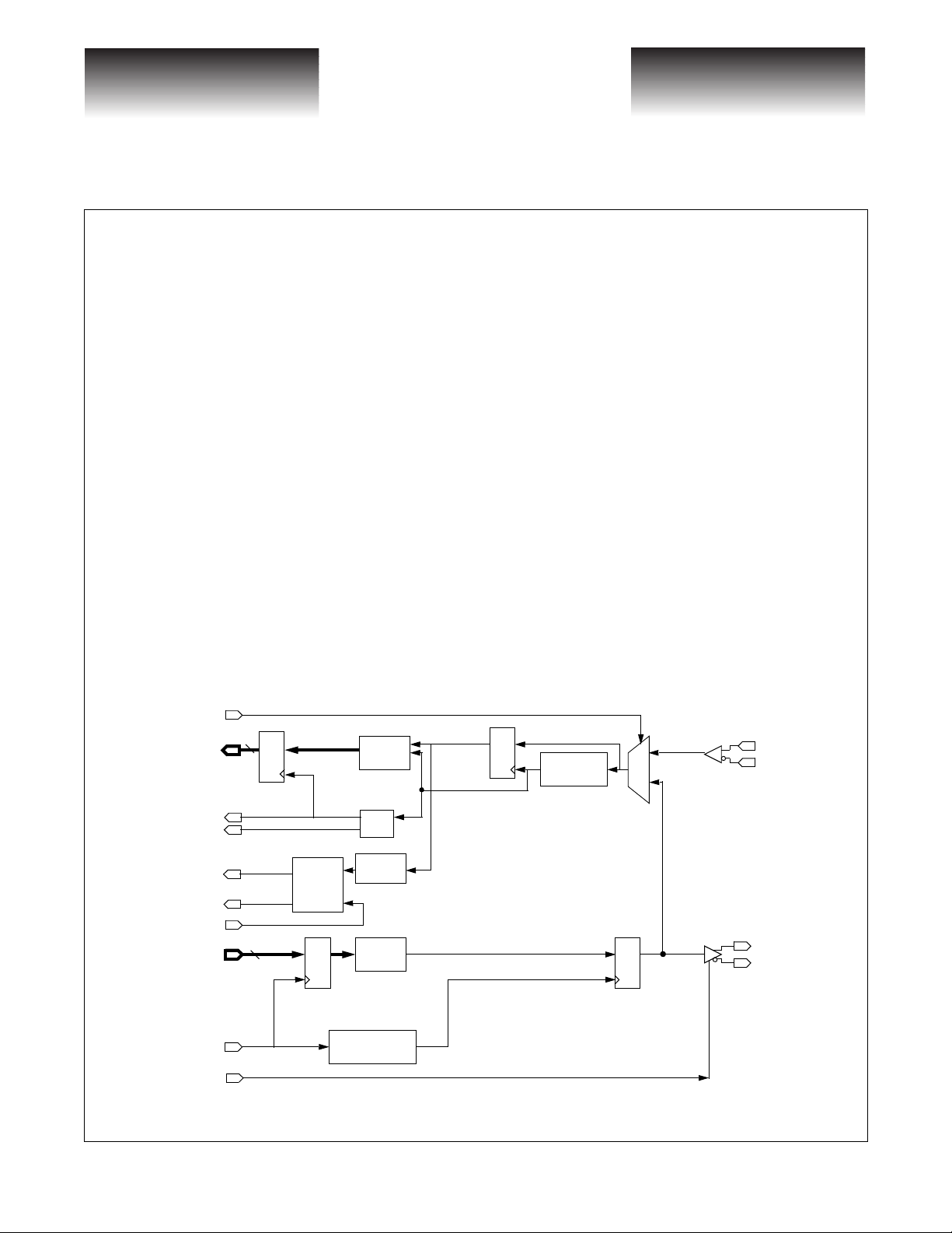
The VSC7126 is a full-speed Fibre Channel Transceiver optimized for Host Adapter and other space- constrained applications. It accepts two 10-bit 8B/10B encoded transmit characters, latches them on the rising edge
of TBC and serializes the data onto the TX+/- PE CL dif ferenti al output s at a baud rate which is twent y times the
TBC frequency. It also samples serial re ceive data o n the RX+/- PE CL differen tial inputs, re covers the clo ck
and data, deserializes it onto two 10-bit receive characters, outpu ts a recovered clocks at one twe ntieth of the
incoming baud rate and detects Fibre Channel “Comma” characters. The VSC7126 contains on-chip PLL circuitry for synthesis of the baud-rate transmit clock, and extraction of the clock from the received serial stream.
These circuits are fully monolithic and require no external components.
VSC7126 Block Diagram
EWRAP
20
R0:19
RBC(0)
RBC(1)
L_UNUSE
COM_DET
EN_CDET
T0:19
TBC
TXEN#
Q D
53.125 MHz
Frame
Logic
20
D Q
53.125 MHz
PLL Clock
Multiply (x20)
Serial to
Parallel
÷ 20
Comma
Detect
Parallel
to Serial
Retimed
Data
Recovered
Clock
Q D
Clock
Recovery
Serial Data
Synthesized
Clock
D Q
2:1
RX+
RX-
TX+
TX-
G52148-0, Rev. 4.3
3/4/99 741 Calle Plano, Camarillo, CA 93012 • 805/388-3700 • FAX: 805/987-5896
VITESSE SEMICONDUCTOR CORPORATION
Page 1
Page 2
VITESSE
SEMICONDUCTOR CORPORATION
.0625 Gbits/sec Fibre
hannel Transceiver
Datasheet
VSC7126
Functional Description
Clock Synthesizer:
The VSC7126 clock synthesizer multiplies the 53.125 MHz reference frequency provided on the TBC pin
by 20 to achieve a baud rate clock at nominally 1.0625 GHz. The clock synthesizer contains a fully monolithic
PLL which does not require any external components.
Serializer:
The VSC7126 accepts TTL input data as tw o parallel 10 bit c haracters o n the T0:19 bus which is latched
into the input latch on the rising edge of TBC. This data will be serialized and transmitted on the TX PECL differential outputs at a baud rate of twenty times the frequency of the TBC inp ut, with bit T0 transmitted first.
User data should be encoded for tr ansmissi on usin g the 8B/ 10B block code descr ibed in th e Fibre C hannel specification, or an equivalent, edge rich, DC-balanced code. If either EWRAP or TXEN# is HIGH the transmitter
will be disabled with TX+ HIGH and TX- LOW. If both EWRAP and TXEN# are LOW, the transmitter outputs
serialized data.
Transmission Character Interface
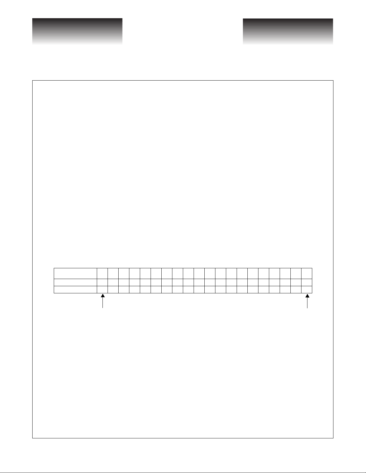
In Fibre Channel, an encoded byte is 10 bits and is referred to as a transmission character. The 20 bit interface on the VSC712 6 corresponds to two transmission characters. This mapping is illustrated in Figure 1.
Figure 1: Transmission Order and Mapping to Fibre Channel Character
Parallel Data Bits 191817161514131211100908070605040302010
8B/10B Bit Position
Valid Comma Position
Last Data Bit Transmitted
Clock Recovery:
The VSC7126 accepts differential high speed serial inputs on the RX+/RX- pins, (when EWRAP is LOW),
extracts the clock and retimes the data. The serial bit stream should be encoded to provide DC balance and limited run length by a Fibre Channel compatible 8B/10B transmitter or equivalent. The VSC7126 clock recovery
circuitry is completely monolithic and requires no external components. For proper operation, the baud rate of
the data stream to be recovered should be within 200 ppm of twenty times the TBC frequency. This allows
oscillators on either end of the link to be 53.125 MHz +/- 100ppm.
Deserializer:
The retimed serial bit stream is converted into two 10-bit parallel output charact ers. The VSC7126 provides
a TTL recovered clock, RBC(0) and its complement RBC(1), at one-twentieth of the serial baud rate. The
clocks are generated by dividing down the high-speed clock which is phase locked to the serial data. The serial
data is retimed by the internal high-speed clock, and deserialized. The resulting parallel data will be captured
j hgfi edcbaj hgf i edcba
1111100
First Data Bit Transmitted
0
Page 2
741 Calle Plano, Camarillo, CA 93012 • 805/388-3700 • FAX: 805/987-5896 3/4/99
VITESSE SEMICONDUCTOR CORPORATION
G52148-0, Rev. 4.3
Page 3

VITESSE
SEMICONDUCTOR CORPORATION
Datasheet
SC7126
by the adjoining protocol logic on the falling edge of RBC(0). In order to maximize the setup and hold times
available at this inte rface, the paral lel data is loaded into the outp ut register at a po int nomina lly midway
between the falling edges of RBC(0).
If serial input data is not pres ent, or does no t meet the requ ired baud rate, th e VS C7126 will continue to
produce a recovered clock so that downstream logic ma y continue to function. In the absence of a signa l, the
RBC(0)/RBC(1) output clocks will immediately lock to the TBC reference clock.
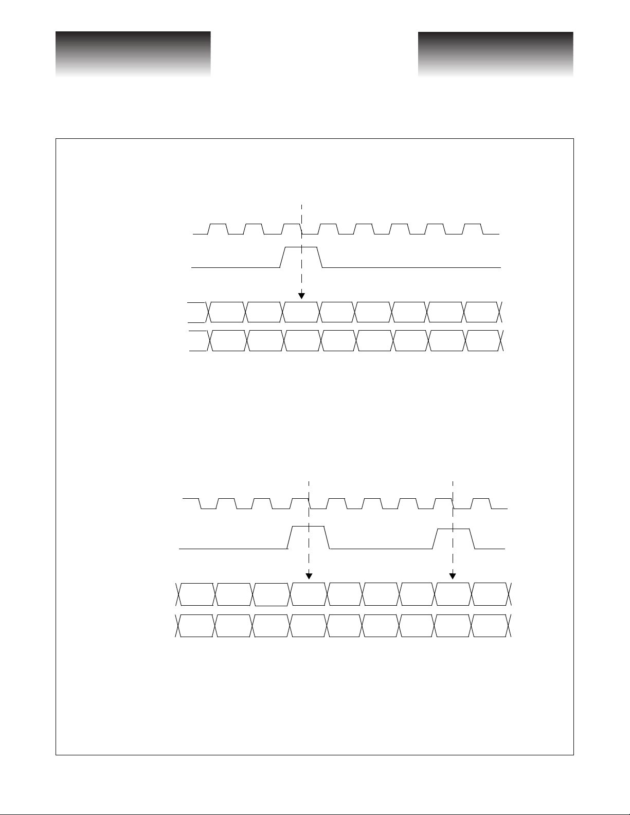
Word Alignment:
The VSC7126 provides 7-bit Fibre Channel comma character recognition and data word alignment. Word
synchronization is enabled by asserting EN_CDET HIGH. When synchronization is enabled, the VSC7126
constantly examines the se rial data for the p resence of the Fibre Channel “c omma” char acter. This pattern is
“0011111XXX”, where the leading zero corresponds to the first bit received. The comma sequence is not contained in any normal 8B/10B coded data character or pair of adjacent characters. It occurs only within special
characters, known as K28.1, K28.5 and K28.7, which are define d specifically for synchro nization in Fibre
Channel systems. Improper alignment of the comma character is defined as any of the following conditions:
1) The comma is not aligned within the 10-bit transmission character such that T0...T6 = “0011111”
2) The comma straddles the boundary between two 10-bit transmission characters.
When EN_CDET is HIGH and an improperly aligned comma is encountered, the internal data is shifted in
such a manner that the comma character is aligned properly in R0:6 as shown in Figure 1. This resul ts in proper
character and word alignment. When the parallel data alignment changes in response to an improperly aligned
comma pattern, some data which would have been presented on the parallel output port may be lost. However,
the synchronization chara cter and subsequent data will b e output correctly and pro perly aligned. When
EN_CDET is LOW, the current alignment of the ser ial dat a is maint ained indef initel y, regardless of data pattern.
On encountering a comma character, COM_DET is driven HIGH to inform the user that realignment of the
parallel data field may have occurred. The COM_DET pulse is presented simultaneously with the comma character and has a duration equal to the data. The COM_DET signal is timed such that it can be captured by the
adjoining protocol logic on the falling edge of RBC(0). Functional waveforms for synchronization are given in
Figure 2 and Figure 3. Figure 2 shows the case when a comma character is detected and no phase adjustment is
necessary. It illustrates the position of the COM_DET pulse in relation to the comma character on R0:6.
Figure 3 shows the case where the K28.5 is det ect ed, b ut it i s o ut of phase and a change in the ou tp ut dat a al i gnment is required. Note that up to three characters prior to the comma character may be corrupted by the realignment process.
1.0625 Gbits/sec Fibre
Channel Transceiver
Signal Detection:
An output, LUNUSE, is provided to signal when the link is open or down. This signal is asserted if R0:19
are all either LOW or HIGH and EWRAP is LOW.
G52148-0, Rev. 4.3
3/4/99 741 Calle Plano, Camarillo, CA 93012 • 805/388-3700 • FAX: 805/987-5896
VITESSE SEMICONDUCTOR CORPORATION
Page 3
Page 4
VITESSE
SEMICONDUCTOR CORPORATION
.0625 Gbits/sec Fibre
hannel Transceiver
Figure 2: Detection of a Properly Aligned Comma Character
RBC(0)
COM_DET
R0:9
R10:19
Datasheet
VSC7126
K28.5 TChar TChar TChar
TChar TChar TChar TChar
TChar: 10 bit Transmission Character
Figure 3: Detection and Resynchronization of an Improperly Aligned Comma
Receiving Two Consecutive K28.5+TChar Transmission Words
RBC(0)
COM_DET
R0:9
R10:19
PC
PC = Potentially Corrupted
K28.5 TChar TChar TChar K28.5 TChar
PCPC
TChar TChar TChar TChar TChar TChar
Page 4
741 Calle Plano, Camarillo, CA 93012 • 805/388-3700 • FAX: 805/987-5896 3/4/99
VITESSE SEMICONDUCTOR CORPORATION
G52148-0, Rev. 4.3
Page 5
VITESSE
SEMICONDUCTOR CORPORATION
Datasheet
SC7126
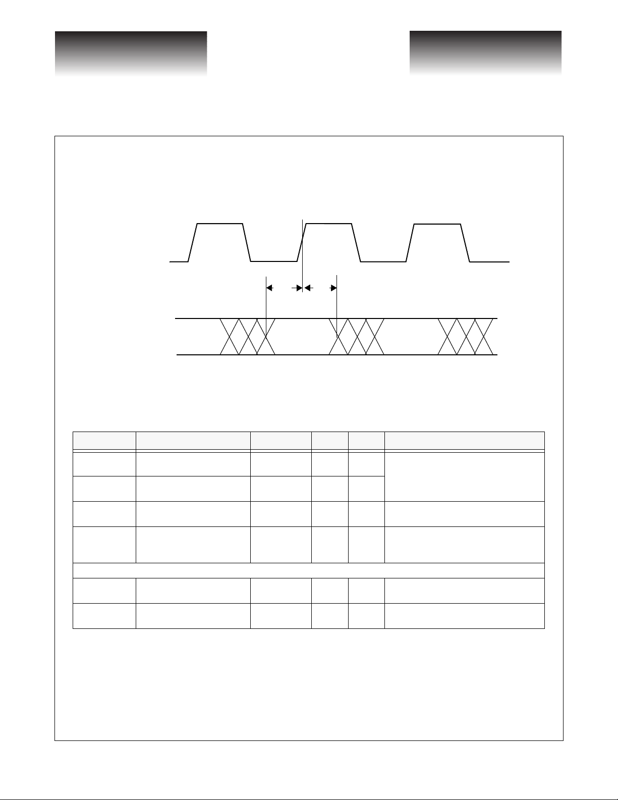
AC Characteristics
TBC
T0:19
20 Bit Data
Data Valid
Figure 4: Transmit Timing Waveforms
T
1
Data Valid
T
2
1.0625 Gbits/sec Fibre
Channel Transceiver
Data Valid
Table 1: Transmit AC Characteristics
Parameters Description Min Max Units Conditions
T
T
T
SDR,TSDF
T
LAT
1
2
T0:19 Setup time to the
rising edge of TBC
T0:19 hold time after the
rising edge of TBC
TX+/TX- rise and fall time — 300 ps.
Latency from rising edge
of TBC to T0 appearing on
TX+/TX-
1.5 —ns.
2.5 — ns.
20 bc - 4 ns ns. bc = Bit Clock Period s
Measured between the valid data level of
T0:19 to the 1.4V point of TBC
20% to 80%, 75 Ohm load to Vdd-2V
Tested on a sample basis
Transmitter Output Jitter Allocation
T
RJ
T
DJ
Serial data output random
jitter (RMS)
Serial data output
deterministic jitter (p-p)
—20ps.
— 120 ps.
RMS, tested on a sample ba s i s
(refer to Figure 8)
Peak to peak, tested on a sample basis
(refer to Figure 8)
G52148-0, Rev. 4.3
3/4/99 741 Calle Plano, Camarillo, CA 93012 • 805/388-3700 • FAX: 805/987-5896
VITESSE SEMICONDUCTOR CORPORATION
Page 5
Page 6

VITESSE
SEMICONDUCTOR CORPORATION
.0625 Gbits/sec Fibre
hannel Transceiver
RBC(0)
RBC(1)
R0:19 &
COM_DET
LUNUSE
Table 2: Receive AC Characteristics
Data Valid
Figure 5: Receive Timing Waveforms
T
3
T
SKEW
T
1
Data Valid Data Valid
T
2
Datasheet
VSC7126
Parameters Description Min. Max. Units Conditions
T
1
T
2
T
4
T
, T
R
R
lat
T
SKEW
T
LOCK
NOTE: Probability of Recovery for data acquisition is 95% per section 5.3 of the FC-PH rev 4.3.
Data or COM_DET Valid
prior to RBC(0) fall
Data or COM_DET Valid
after RBC(0) fall
Deviation of RBC(0) falling
edge to falling edge delay
from nominal.
R0:19, COM_DET, RBC(0)
F
rise and fall time
Latency from RX to RBC(0)
falling and RO valid.
Skew between edges of
RBC(0) and RBC(1)
Data acquisition lock time @
1.0625Gb/s
4 —ns.
6.0 — ns.
-500 500 ps.
0.7 2.4 ns.
40 bc + 10 ns 59 bc + 10 ns
---- 1.5 ns
—2.4
Clocks
Bit
µs.
Measured between t he 1.4V
point of RBC(0) and a valid
level of R0:19 or
COM_DET. All outputs
driving 10pF load.
Nominal delay is 20 bit
times.
Tested on sample basis
Between V
, into 10 pf. load.
V
ih(min)
bc = bit clock periods
8B/10B IDLE pattern.
Tested on a sample basis
il(max)
and
Page 6
741 Calle Plano, Camarillo, CA 93012 • 805/388-3700 • FAX: 805/987-5896 3/4/99
VITESSE SEMICONDUCTOR CORPORATION
G52148-0, Rev. 4.3
Page 7

VITESSE
SEMICONDUCTOR CORPORATION
Datasheet
SC7126
Figure 6: TBC Timing Waveforms
T
H
TBC
T
L
Table 3: Reference Clock Requirements
Parameters Description Min Max Units Conditions
Range over which both transmit an d receive
FR Frequency Range 50 55 M Hz
reference clocks on any link may be centered
1.0625 Gbits/sec Fibre
Channel Transceiver
V
ih(min)
V
il(max)
Mean frequency offset between transmit and
FO Frequency Offset -200 200 ppm.
T
L,TH
DC TBC duty cycle 30 70 % Measured at 1.5V
T
RCR,TRCF
J
T
Pulse Width, Low / High 4 .5 ---- ns
TBC rise and fall time ---- 2.0 ns. Between V
T ot al jitter tolera n ce on
REFCLK
---- 120 ps
receive reference clocks on one link
Low is measured from Vil(max) to Vil(max),
High is measured from V
Peak-to-peak total jitter for frequencies
between 50KHz and 7MHz
il(max)
and V
(min) to Vih(min)
ih
ih(min)
G52148-0, Rev. 4.3
3/4/99 741 Calle Plano, Camarillo, CA 93012 • 805/388-3700 • FAX: 805/987-5896
VITESSE SEMICONDUCTOR CORPORATION
Page 7
Page 8

VITESSE
SEMICONDUCTOR CORPORATION
.0625 Gbits/sec Fibre
hannel Transceiver
DC Characteristics
Parameters Description Min Typ Max Units Conditions
∆V
∆V
V
OH
V
OL
OUT75
OUT50
∆V
V
V
I
IH
I
IL
V
DD
P
I
DD
IN
IH
IL
D
Output HIGH voltage (TTL) 2.4 2.9 —VIOH = -1.0 mA
Output LOW voltage (TTL) — — 0.5 V IOL = +1.0 mA
Serial Output vol tage
differential peak-to-peak swing
(TX+/TX-)
Serial Output vol tage
differential peak-to-peak swing
(TX+/TX-)
Serial Input voltage differential
peak-to-peak swing (RX+/RX-)
Input HIGH voltage (TTL) 2.0 — 5.5 V
Input LOW voltage (TTL) 0 — 0.8 V —
Input HIGH current (TTL) — 50 500 µAVIN = 2.4 V
Input LOW current (TTL) — — -500 µAVIN = 0.5 V
Supply voltage 3.14 — 3.47 V 3. 3V±5%
Power dissipation — 850 1560 mW
Supply Curren t — 245 450 mA
(Over recommended operating conditions).
1200 — 2200 mV 75Ω to V
1000 — 2200 mV 50Ω to V
400 — 3200 mV
Outputs open,
V
= VDD max
DD
Outputs open,
V
= VDD max
DD
Datasheet
VSC7126
– 2.0 V
DD
– 2.0 V
DD
Absolute Maximum Ratings
(1)
Power Supply Voltage, (VDD)............................................................................................................-0.5V to +4V
DC Input Voltage (PECL inputs)............................................................................................-0.5V to V
DD
+0.5V
DC Input Voltage (TTL inputs) .........................................................................................................-0.5V to 5.5V
DC Output Voltage (TTL Outputs)........................................................................................ -0.5V to V
+ 0.5V
DD
Output Current (TTL Outputs)................................................................................................................. +/-50mA
Output Current (PECL Outputs)................................................................................................................+/-50mA
o
Case Temperature Under Bias.........................................................................................................-55
Storage Temperature.....................................................................................................................-65
to +125oC
o
C to +150oC
Maximum Input ESD (Human Body Model)............................................................................................... 1500V
Recommended Operating Conditions
Power Supply Voltage, (VDD)................................................................................................................+3.3V+5%
o
Operating T emp eratur e Range ................................................. ........ .......0
Notes:
(1) CAUTION: Stresses listed under “Absolute Maximum Ratings” may be applied to devices one at a tim e without causing
permanent damage. Functionality at or above the values listed is not implied. Exposure to these values for extended
periods may affect device reliability.
C Ambient to 90oC Case Temperature
Page 8
741 Calle Plano, Camarillo, CA 93012 • 805/388-3700 • FAX: 805/987-5896 3/4/99
VITESSE SEMICONDUCTOR CORPORATION
G52148-0, Rev. 4.3
Page 9

VITESSE
SEMICONDUCTOR CORPORATION
Datasheet
SC7126
1.0625 Gbits/sec Fibre
Channel Transceiver
Figure 7: Parametric Measurement Information
Serial Input Rise and Fall Time TTL Input and Output Rise and Fall Time
V
80%
20%
T
r
Receiver Input Eye Diagram Jitter Tolerance Mask
T
f
Bit Time
T
r
T
f
ih(min)
V
il(max)
Amplitude
Parametric Test Load Circuit
Serial Output Load
Z0 = 75Ω
V
DD
75Ω
– 2.0V
Total jitter tolerance is
0.7UI, according to
Fibre Channel 4.3 Annex J
Eye Width%
TTL A.C. Output Load
10 pF
G52148-0, Rev. 4.3
3/4/99 741 Calle Plano, Camarillo, CA 93012 • 805/388-3700 • FAX: 805/987-5896
VITESSE SEMICONDUCTOR CORPORATION
Page 9
Page 10

VITESSE
SEMICONDUCTOR CORPORATION
.0625 Gbits/sec Fibre
hannel Transceiver
BERT
Pattern
Generator
CLK = 1.0625 GHz
DATA = 00000 0 000011111 11111
0011111000 0011111000
Random jitter (RJ) measurements performed according to Fibre Channel 4.3 Annex A, Test Methods, Section
A.4.4. Measure standard deviation of all 50% crossing points. Peak to peak RJ is +
Figure 8: Transmitter Jitter Measurement Method
Random Jitter Measurement
RJ
-K28.7 -K28.7
DATA
DATA
53.125MHz
53.125MHz
VSC7126
TBC
T00:19
TX
TX+
TX-
Trigger
1.0625 Gbit/s
Single-Ended Measurement
Datasheet
VSC7126
Digitizing
Scope
7 sigma of distributi on.
BERT
Pattern
Generator
CLK = 1.0625 GHz
DAT A = 00000 0000011111 11111
DJ
TRIGGER
DATA
-K28.5 +K28.5
0011111010 1100000101
2 bit time
Deterministic Jitter Measurement
DATA
PAT SYNC
8 bit time
7 bit time
53.125
53.125MHz
12 bit time
10 bit time
9 bit time
VSC7126
TX
TBC
T0:19
TX+
TX-
19 bit time
18 bit time
17 bit time
Trigger
1.0625 Gbit/s
Single-Ended Measurement
surements performed accordi ng to
20 bit time
Fibre Channel 4.3 Annex A, Test
Methods, Section A. 4.3. Measure
time of all the 50% points of all ten
transitions. DJ is the range of the
timing variation fro m expe cted .
Digitizing
Scope
Deterministic jitter (DJ) mea-
Page 10
741 Calle Plano, Camarillo, CA 93012 • 805/388-3700 • FAX: 805/987-5896 3/4/99
VITESSE SEMICONDUCTOR CORPORATION
G52148-0, Rev. 4.3
Page 11

VITESSE
SEMICONDUCTOR CORPORATION
Datasheet
SC7126
Input Structures
INPUT
Figure 9: Input Structures
+3.3 V
V
DD
Current
Limit
R
R
1.0625 Gbits/sec Fibre
Channel Transceiver
INPUT
INPUT
GND
TBC and TTL Inputs
A
V
DD
+3.3 V
GND
High Speed Differential Input
(RX+/RX-)
B
All Resistors
3.3K
G52148-0, Rev. 4.3
3/4/99 741 Calle Plano, Camarillo, CA 93012 • 805/388-3700 • FAX: 805/987-5896
VITESSE SEMICONDUCTOR CORPORATION
Page 11
Page 12

VITESSE
SEMICONDUCTOR CORPORATION
.0625 Gbits/sec Fibre
hannel Transceiver
Package Pin Descriptions
Datasheet
VSC7126
Figure 10: Pin Diagram
Table 4: Pin Identification
Pin # Name Description
2,4,6,9,11,14,
16,18,20,23,3,
5,8,10,12,15,
17,19,22,24
31 TBC
79
77
Page 12
T0:19
TX+
TX-
741 Calle Plano, Camarillo, CA 93012 • 805/388-3700 • FAX: 805/987-5896 3/4/99
Transmit Data Bus, Bits 0 thru 19. INPUTS - TTL
20-bit transmit character. Parallel data on this bus is clocked in on the rising edge of
TBC. The data bit corresponding to T0 is transmitted first.
Transmit Byte Clock. INPUT - TTL
This rising edge of this clock latches T0:9 into the input register. It also provides the
reference clock, at one twentieth of the baud rate to the PLL.
Transmitter Serial Outputs. OUTPUTS - Differential PECL
These pins output the serialized tran smit data whe n EWRAP is LOW. When EWRAP is
HIGH, TX+ is HIGH and TX- is LOW. (AC Coupling reco mmended)
VITESSE SEMICONDUCTOR CORPORATION
G52148-0, Rev. 4.3
Page 13

VITESSE
SEMICONDUCTOR CORPORATION
Datasheet
SC7126
Pin # Name Description
65,63,59,57,
55,52,50,48,
45,43,64,62,
58,56,54,51,
49,47,44,42
34 EWRAP
70
69
39
38
27 EN_CDET
37 COMDET
35 TXEN#
66 LUNUSE
26
28
29
1,21,30,68,72 VSS Digital Ground
40,41,60,61 VSST Digital Ground for TTL Outputs
74 VSSA Analog Ground
7,13,25,32,33,
67,71,75
36,46,53 VDDT Digital Power for TTL outputs (3.3V)
76,80 VDDP Digital Power for PECL outputs (3.3V)
73 VDDA Analog Power (3.3V)
78 N/C Not Internally Connected.
R0:19
RX+
RX-
RBC(0)
RBC(1)
TEST1
TEST2
TEST3
VDD Digital Power (3.3V)
Receive Data Bus, Bits 0 thru 19 OUTPUTS - TTL
20-bit received character. Parallel data on this bus i s clocked out on the rising edge of
RBC(0). R0 is the first bit received on RX+/RX-.
Enable Internal WRAP Mode. INPUT - TTL
LOW for Normal Operation. When HIGH, an internal loopback path from the
transmitter to the receiver is enabled, TX+ = HIGH and TX- is LOW.
Receive Serial Inputs INPUTS - Differential PECL
The receiver inputs when EWRAP is LOW. Internally biased to VDD/2, with 3.3KΩ
resistors to VDD and GND. (AC Coupling recommended)
Recovered Byte Clock and Complement OUTPUT - TTL
Recovered cl ock and co mplemen t derive d from on e twentieth of the RX+/ - data s tream.
The rising edge of RBC(0) corresponds to a new word on R0:19.
ENable Comma DETect. INPUT - TTL
Enables comma detection and word resynchronization when HIGH. When LOW, keeps
current word alignment and disables comma detection.
COMma DETect OUTPUT - TTL
This output goes HIGH to indicate that R0:6 contains a Comma Character (‘001111 1’).
COMDET will go HIGH only during a cycle when RBC(0) is falling. COMDET is
enabled by EN_CDET being HIGH.
Transmitter ENable INPUT - TTL
When LOW , the TX outputs transmit serial data. When HIGH, the TX+ is HIGH and the
TX- is LOW.
Link UNUSE OUTPUT - TTL
Normally is LOW. If R0:19 is all LOW or all HIGH and EWRAP is LOW, this output
will be asserted HIGH to indicate an open link on RX+/-.
TEST Mode Pins INPUT - TTL
Factory test pins . Tie to VDD for normal operation.
1.0625 Gbits/sec Fibre
Channel Transceiver
G52148-0, Rev. 4.3
3/4/99 741 Calle Plano, Camarillo, CA 93012 • 805/388-3700 • FAX: 805/987-5896
VITESSE SEMICONDUCTOR CORPORATION
Page 13
Page 14

VITESSE
SEMICONDUCTOR CORPORATION
.0625 Gbits/sec Fibre
hannel Transceiver
Package Information
80 61
1
20
Datasheet
VSC7126
80-pin PQFP Package Drawing
F
G
60
IH
41
Item 14 mm T olerance
A2.35 MAX
D 2.00 +0.10/-0.05
E0.30 ±.05
F 17.20 ±.25
G 14.00 ±.10
H 17.20 ±.25
I 14.00 ±.10
J 0 .88 +.15/-.10
K0.65BASIC
21 40
10° TYP
A
10° TYP
NOTES:
Drawing not to scale.
All units in mm unless otherwise noted.
K
A
0.17 MAX.
D
0.30 RAD. TYP
0.20 RAD. TYP.
0.25
J
.
STANDOFF
0.25 MAX.
0.102 MAX LEAD
COPLANARITY
0° - 8°
E
Page 14
741 Calle Plano, Camarillo, CA 93012 • 805/388-3700 • FAX: 805/987-5896 3/4/99
VITESSE SEMICONDUCTOR CORPORATION
G52148-0, Rev. 4.3
Page 15

VITESSE
SEMICONDUCTOR CORPORATION
Datasheet
SC7126
1.0625 Gbits/sec Fibre
Channel Transceiver
Package Thermal Characteristics
The VSC7126 is packaged in a 14 mm PQFP with an integrated heat spreader. These packages use industry-standard EIAJ footprints, but have been enhanced to improve therma l dissipation. The construction of the
packages is as shown in Figure 11.
Figure 11: Package Cross Section - 14 mm package
Plastic Molding Compound
Lead
Table 5: Thermal Resistance
Symbol Description 14mm Value Units
θ
jc
θ
ca
θ
ca-100
θ
ca-200
θ
ca-400
θ
ca-600
Thermal resistance from junction to case 17
Thermal resistance from case to ambient in still air including
conduction through the leads.
Thermal resistance from case to ambient with 100 LFM airflow 28
Thermal resistance from case to ambient with200 LFM airflow 25
Thermal resistance from case to ambient with 400 LFM airflow 22
Thermal resistance from case to ambient with 600 LFM airflow 20
Bond Wire
Copper Heat Spreader
Die
32
o
C/W
o
C/W
o
C/W
o
C/W
o
C/W
o
C/W
The VSC7126 is designed to operate with a case temperature up to 90oC. The user must guarantee that the
temperature specification is not violated. With the Thermal Resistances shown above, the 14x14 PQFP can
o
operate in still air ambient temperatures of 40
C (40°C = 90°C - 1.56W * 32°C/W). If the ambient air tempera-
ture exceeds these limits, then some form of cooling through a heatsi nk or an i ncrease in ai rflo w wil l be needed.
Moisture Sensitivity Level
This device is rated with a moisture sensitivity level 3 rating. Refer to Application Note AN-20 for appropriate handling procedures.
G52148-0, Rev. 4.3
3/4/99 741 Calle Plano, Camarillo, CA 93012 • 805/388-3700 • FAX: 805/987-5896
VITESSE SEMICONDUCTOR CORPORATION
Page 15
Page 16

VITESSE
SEMICONDUCTOR CORPORATION
.0625 Gbits/sec Fibre
hannel Transceiver
Ordering Information
The order number for this product is formed by a combination of the device number, and package type.
Device Type
VSC7126: 1.0625 Gbps Transceiver
Package Style
QX: 80-pin, 14 x 14 mm PQFP
VSC7126
Datasheet
VSC7126
QX
Notice
Vitesse Semiconductor Corporation reserves the right to make changes in its products, specifications or
other information at any time without prior notice. Therefore the reader is cautioned to confirmation that this
datasheet is current prior to placing any orders. The company assumes no responsibility for any circuitry
described other than circuitry entirely embodied in a Vitesse product.
Warning
Vitesse Semiconductor Corporation’s product are not intended for use in life support appliances, devices or systems.
Use of a Vitesse product in such applications without written consent is prohibited.
Page 16
741 Calle Plano, Camarillo, CA 93012 • 805/388-3700 • FAX: 805/987-5896 3/4/99
VITESSE SEMICONDUCTOR CORPORATION
G52148-0, Rev. 4.3
 Loading...