

Page 1
V
E
L
O
C
I
T
Y
T
M
VITESSE
SEMICONDUCTOR CORPORATION
Advance Product Information
VSC7123 - Extended Temperature Range
10-Bit Transceiver for Fibre
Channel and Gigabit Ethernet
G52312-0, Rev 2.2 Page 1
04/05/01
© VITESSE SEMICONDUCTOR CORPORATION • 741 Calle Plano • Camarillo, CA 93012
Tel: (800) VITESSE • FAX: (805) 987-5896 • Email: prodinfo@vitesse.com
Internet: www.vitesse.com
Features
General Description
The VSC7123 Extended Temperature Range (ETR) is a full-speed Fibre Channel and Gigabit Ethernet
Transceiver with industry-standard pinouts, which operates down to
−40
o
. The VSC7123 ETR accepts 10-bit
8B/10B encoded transmit data, latches i t on the ri sin g edge of REFCLK and seri ali zes i t onto the TX PEC L differential outputs at a ba ud rate wh ich is 10 t imes the REFCLK frequenc y. Serial da ta input on the RX PEC L differential inputs is resampled by the Clock Recovery Unit (CRU) and deserialized onto the 10-bit receive data
bus synchronously to complementary divide-by-twenty clocks. The VSC7123 ETR receiver detects “Comma”
characters for frame alignment. An analog/digital signal detection circuit indicates that a valid signal is present
on the RX input. A cable equalizer compensates for InterSymbol Interference (ISI) in order to increase maximum cable distances.
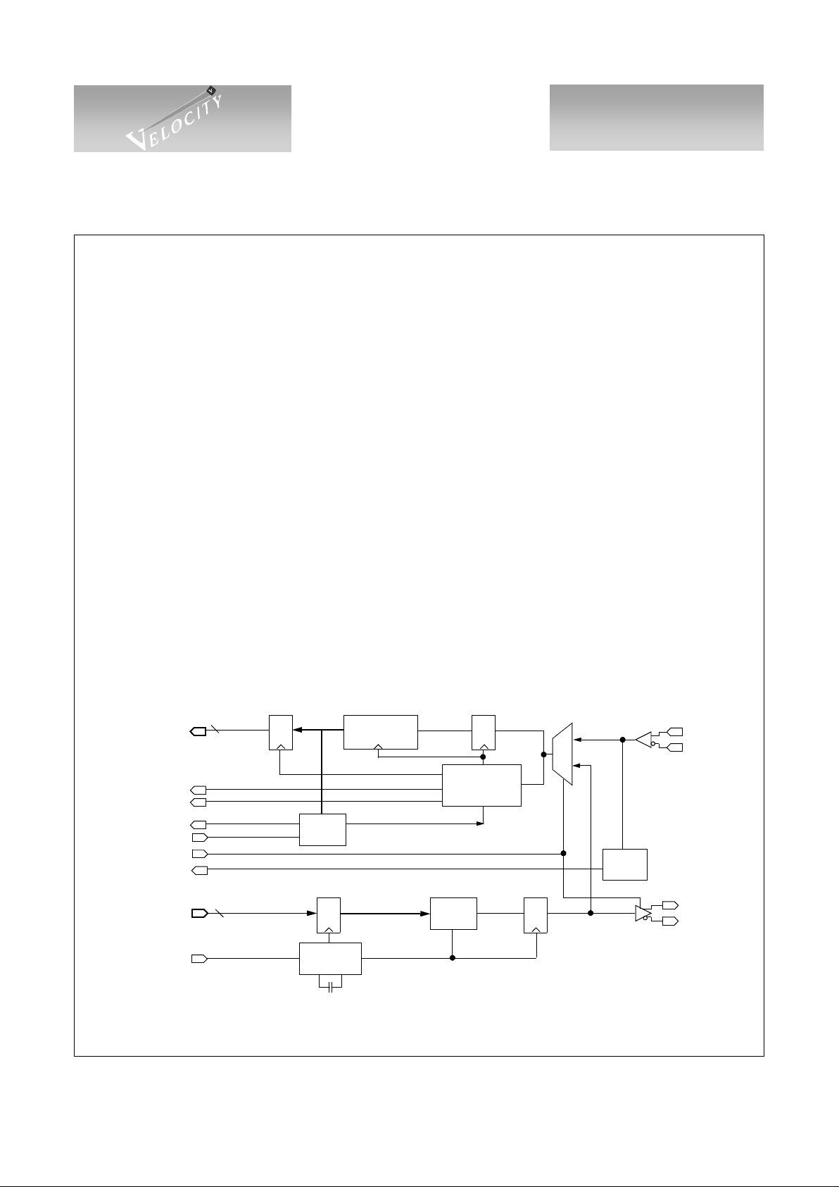
VSC7123 ETR Block Diagram
• 802.3z Gigabit Ethernet Compliant 1. 25 Gb/ s
Transceiver
• ANSI X3T11 Fibre Channel Compliant
1.0625 Gb/s Transceiver
• 0.98 Gb/s to 1.36 Gb/s Ful l -Dupl ex Oper ati on
• 10-Bit TTL Interface for Transmit and
Receive Data
• Operating Temperature Down to -40
o
• RX Cable Equalization
• Analog/Digital Signal Detection
• JTAG Access Port for Testability
• 64-Pin, 10 mm TQFP Package
• Single +3.3V Supply, 650mW Typical
RX+
RX-
Q D
Serial to
Parallel
Clock
Recovery
÷10
Comma
R(0:9)
COMDET
ENCDET
T(0:9)
x10 Clock
Multiply
Parallel
to Serial
TX+
TX-
EWRAP
÷20
RCLK
10
10
2:1
RCLKN
REFCLK
Signal
Detect
Q D
QD
Detect
SIGDET
D QD Q
NOT SHOWN: JTAG Boundary Scan
Page 2

V
E
L
O
C
I
T
Y
T
M
VITESSE
SEMICONDUCTOR CORPORATION
Advance Product Information
10-Bit Transceiver for Fibre
Channel and Gigabit Ethernet
Extended Temperature Ra nge - VSC7123
Page 2 G52312-0, Rev 2.2
04/05/01
© VITESSE SEMICONDUCTOR CORPORATION • 741 Ca ll e Pl an o • Camarillo, CA 93012
Tel: (800) VITESSE • FAX: (805) 987-5896 • Email: prodinfo@vitesse.com
Internet: www.vitesse.com
Functional Description
Clock Synthesizer
The VSC7123 ETR clock synthesizer multiplies the reference frequency provided on the REFCLK pin by
10 to achieve a baud rate clock be tween 0.98GH z and 1.36GHz. The on-chip Pha se Lock Loop (PLL) use s a
single external 0.1
µF capacitor to control the Loop Filter.
Serializer
The VSC7123 ETR accepts TTL input data as a parallel 10 bit character on the T(0:9) bus, which is latched
into the input register on the rising edge of REFCLK. This data is serialized and transmitted on the TX PECL
differential outputs at a baud rate that is 10 times the frequency of the REFCLK, with bit T0 transmitted first.
User data should be encoded using 8B/10B block code or equivalent.
Transmission Character Interface
An encoded byte is 10 bits and is referred to as a transmission character. The 10-bit interface on the
VSC7123 ETR corresponds to a transmission character. This mapping is shown in Figure 1.
Figure 1: Transmission Order and Mapping of an 8B/10B Character
Clock Recovery
The VSC7123 ETR accepts differential high-speed serial inputs on the RX+/RX- pin s, extracts the clock
and retimes the data. Equalizers are included in the receiver to open the data eye and compensate for InterSymbol Interference which may be pres ent in the incoming data. The se rial bit stream should be encoded so as to
provide DC balance and limited run length by an 8B/10B encoding scheme. The CRU is completely monolithic
and requires no external components. For proper operation, the baud rate of the data stream to be recovered
should be within +
200ppm of 10 times the REFCLK frequency. For example, Gigabit Ethernet systems would
use 125MHz oscillators with a
±100ppm accuracy resulting in ±200ppm between VSC7123 ETR pairs.
Deserializer
The recovered serial bit stream is converted into a 10-bit parallel output character. The VSC7123 ETR provides complementary TTL recovered clocks, RCLK and RCLKN, which are 1/20
th
of the serial baud rate. The
clocks are generated by dividing down the high-speed recovered clock which is phase-locked to the serial data.
The serial data is retimed, deserialized and out pu t on R(0 :9). T he paral lel dat a wil l be capture d by the adj oi ni ng
protocol logic on the rising edges of RCLK and RCLKN.
First Data Bit Transmitted
Last Data Bit Transmitted
Parallel Data Bits
8B/10B Bit Position
T9 T8 T7 T6 T5 T4 T3 T2 T1 T0
j hgfi edcba
Comma Character
XXX1111100
Page 3

V
E
L
O
C
I
T
Y
T
M
VITESSE
SEMICONDUCTOR CORPORATION
Advance Product Information
VSC7123 - Extended Temperature Range
10-Bit Transceiver for Fibre
Channel and Gigabit Ethernet
G52312-0, Rev 2.2 Page 3
04/05/01
© VITESSE SEMICONDUCTOR CORPORATION • 741 Calle Plano • Camarillo, CA 93012
Tel: (800) VITESSE • FAX: (805) 987-5896 • Email: prodinfo@vitesse.com
Internet: www.vitesse.com
If serial input data is not present, or does not meet the required baud rate, the VSC7123 ETR will continue
to produce a recovered clo ck, a ll owing downstream logic functionalilty t o co nt in ue. T he RCLK/ RCLKN output
frequency under these circumstances will differ from its expected frequency by no more than +
1%.
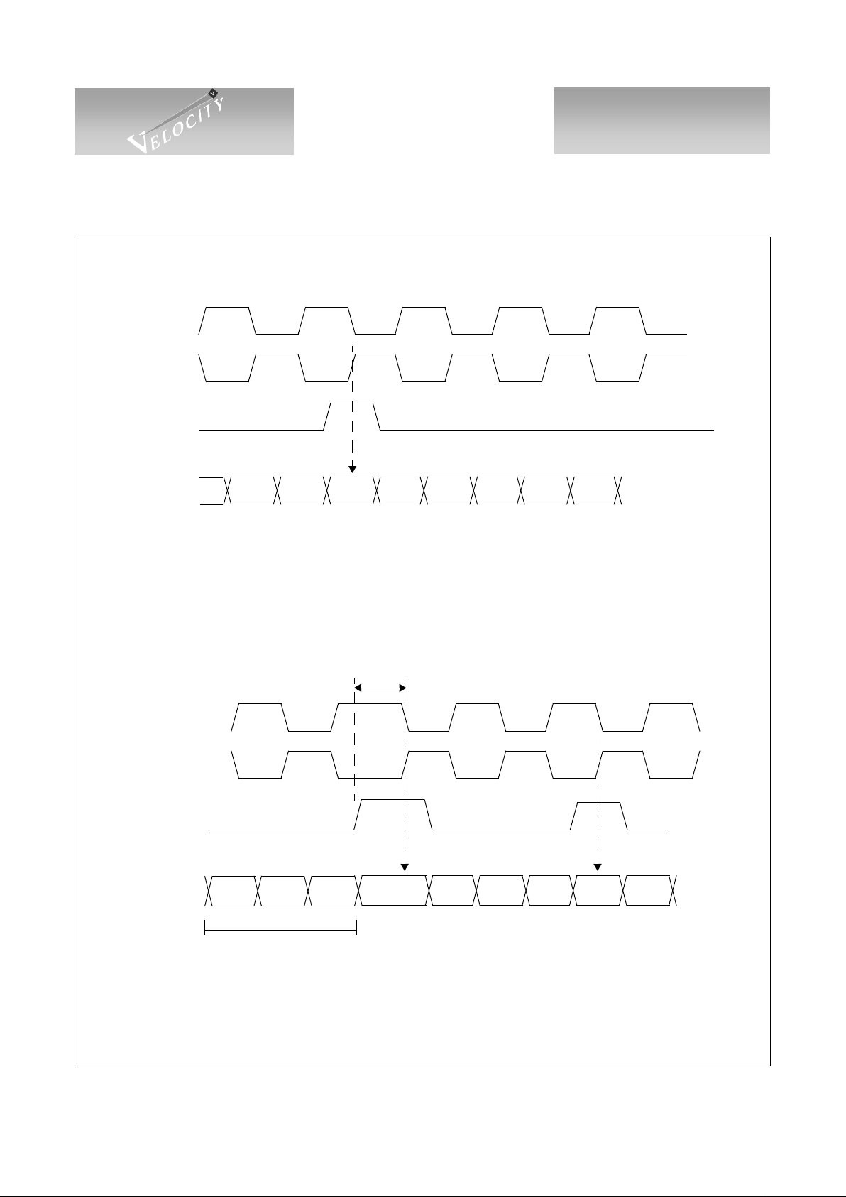
Word Alignment
The VSC7123 ETR provides 7-bit comma character rec ogni tio n an d dat a wo rd al ignment . Word synchron ization is enabled by asserting ENCDET HIGH. When synchronization is enabled, the receiver examines the
recovered serial data for the presence of the “Comma” character. This pattern is “0011111XXX”, where the
leading zero corresponds to the first bit received. The comma sequence is not contained in any normal 8B/10B
coded data character or pair of adjacent characters. It occurs only within special characters, known as K28.1,
K28.5 and K28.7, which are defined for synchronization purposes. Improper alignment of the “Comma” character is defined as any of the following conditions:
1) The comma is not aligned within the 10-bit transmission character such that R0...R6 = “0011111”.
2) The comma straddles the boundary between two 10-bit transmission characters.
3) The comma is properly aligned but occurs in the received character presented during the rising edge of
RCLK rather than RCLKN.
When ENCDET is HIGH and an improperly aligned comma is encountered, the recovered clock is
stretched (never slivered) so that the comma character and recovered clocks are properly aligned to R(0:9). This
results in proper character and word alignment. When the parallel data alignment changes in response to an
improperly aligned comma p att er n, some d a ta whi ch wo ul d have been presented on the paral le l out put p ort may
be lost. Additionally, the first Comma patt er n may also b e lo st or co rru pt ed. Su bsequent data will be output correctly and properly aligned. When ENCDET is LOW, the current alignment of the serial data is maintained
indefinitely, regardless of data pattern.
On encountering a comma character, COMDET is driven HIGH. The COMDET pulse is presented simultaneously with the comma charact er and has a duration equal to the dat a, or ha lf of an R CLK per iod. The COMDET signal is timed such that it can be captured by the adjoining protocol logic on the rising edge of RCLKN.
Functional waveforms for synchronization are given in Figure 2 and Figure 3. Figure 2 shows the case when a
comma character is detected and no phase adjust ment is necessary. It illustrates the position of the COMDET
pulse in relation to the comma character on R(0:9). Figure 3 shows the case where the K28.5 is detected, but it
is misaligned so a change in the output data alignment is required. Note that up to three characters prior to the
comma character may be corrupted by the realignment process.
Page 4
V
E
L
O
C
I
T
Y
T
M
VITESSE
SEMICONDUCTOR CORPORATION
Advance Product Information
10-Bit Transceiver for Fibre
Channel and Gigabit Ethernet
Extended Temperature Ra nge - VSC7123
Page 4 G52312-0, Rev 2.2
04/05/01
© VITESSE SEMICONDUCTOR CORPORATION • 741 Ca ll e Pl an o • Camarillo, CA 93012
Tel: (800) VITESSE • FAX: (805) 987-5896 • Email: prodinfo@vitesse.com
Internet: www.vitesse.com
Figure 2: Detection of a Properly Aligned Comma Character
Figure 3: Detection and Resynchronization of an Improperly Aligned Comma Character
TChar: 10 bit Transmission Character
COMDET
R(0:9)
RCLK
RCLKN
K28.5 TChar TChar TChar
COMDET
Receiving Two Consecutive K28.5+TChar Transmission Words
K28.5 TChar TChar TChar K28.5 TChar
Potentially Corrupted
R(0:9)
RCLK
RCLKN
Clock Stretching
TChar: 10 bit Transmission Character
Page 5

V
E
L
O
C
I
T
Y
T
M
VITESSE
SEMICONDUCTOR CORPORATION
Advance Product Information
VSC7123 - Extended Temperature Range
10-Bit Transceiver for Fibre
Channel and Gigabit Ethernet
G52312-0, Rev 2.2 Page 5
04/05/01
© VITESSE SEMICONDUCTOR CORPORATION • 741 Calle Plano • Camarillo, CA 93012
Tel: (800) VITESSE • FAX: (805) 987-5896 • Email: prodinfo@vitesse.com
Internet: www.vitesse.com
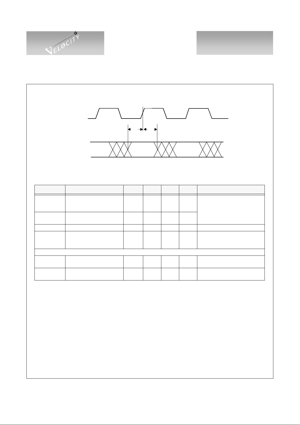
Signal Detection
The receiver has an output, SIGDET, indicating, when HIGH, that the RX input contains a valid Fibre
Channel or Gigabit Ethernet signal. A combination of one analog and three digital checks are used to determi ne
if the incoming signal contains valid data. SIGDET is updated every four RCLKs. During the current period, if
all four of the following criteria are met, SIGDET will be HIGH during the next 4-RCLK period. If any of the
four criteria is not met during the current period, SIGDET will be LOW during the next 4-RCLK period.
1) Analog transition detection is performed on the input to verify that the signal swings are of adequate
amplitude. The RX+/- input buffer contains a differential voltage comparator which will go high if the
differential peak-to-peak amplitude is greater than 400mV or LOW if under 20 0mV. If the amplitude is
between 200 and 400mV, the output is indeterminate.
2) Data on R(0:9) is monitored for all zeros (0000000000). If this pattern is encountered during the current
RCLK interval, the SIGDET output will go LOW du ring the next 4-RCLK interval.
3) Data on R(0:9) is monitored for all ones (1111111111). If this pattern is encountered during the current
RCLK interval, the SIGDET output will go LOW du ring the next 4-RCLK interval.
4) Data on R(0:9) is monitored for K28.5- (0011111010). Unlike previous patterns, the interval during
which a K28.5- must occur is 64K+24 10-bit characters in length. Valid Fibre Channel or Gigabit Ethernet data will contain a K28.5- character during any period of this length. If a K28.5- is not detected during the monitoring period, SIGDET will go LOW during the next period.
The behavior of SIGDET is affected by EWRAP and ENCDET as shown in Table 1.
Table 1: Signal Detect Behavior
NOTE: COMDET, RCLK, RCLKN and R(0:9) are unaltered by SIGDET.
JTAG Access Port
A JTAG Access Port is provided to assist in board-level testing. Through this port most pins can be
accessed or controlled and all TTL outputs can be tri-stated. A full description of the JTAG functions on this
device is available in “VSC7123/VSC7133 JTAG Access Port Functionality.”
EWRAP ENCDET COMDET
Transition
Detect
All Zeros/
All Ones
K28.5
Presence
Mode
0 0 Disabled Enabled Enabled Enabled Normal
0 1 Enabled Enabled Enabled Disabled SIGDET ignores commas
1 0 Disabled Enabled Disabled Disabled Loopback
1 1 Enabled Enabled Disabled Disabled Loopback
Page 6
V
E
L
O
C
I
T
Y
T
M
VITESSE
SEMICONDUCTOR CORPORATION
Advance Product Information
10-Bit Transceiver for Fibre
Channel and Gigabit Ethernet
Extended Temperature Ra nge - VSC7123
Page 6 G52312-0, Rev 2.2
04/05/01
© VITESSE SEMICONDUCTOR CORPORATION • 741 Ca ll e Pl an o • Camarillo, CA 93012
Tel: (800) VITESSE • FAX: (805) 987-5896 • Email: prodinfo@vitesse.com
Internet: www.vitesse.com
Figure 4: Transmit Timing Waveforms
Table 2: Transmit AC Characteristics
Parameters Description Min Typ Max Units Conditions
T
1
T(0:9) Setup time to the
rising edge of REFCLK
1.5 ——ns
Measured between the valid data
level of T(0:9) to the 1.4V point o f
REFCLK
T
2
T(0:9) hold time after the
rising edge of REFCLK
1.0 ——ns
T
SDR,TSDF
TX+/TX- rise and fall time ——300 ps 20% to 80%, 50Ω load to VDD- 2.0
T
LAT
Latency from rising edge of
REFCLK to T0 appearing on
TX+/TX-
8bc —
8bc+
4ns
ns
bc = bit clocks
ns = nano second
Transmitter Output Jitter Allo catio n
RJ Random jitter (RMS) — 58ps
Measured at SO+/-, 1 sigma
deviation of 50% crossing point.
DJ
Serial data output
deterministic jitter (pk-pk)
— 30 80 ps
IEEE 802.3Z Clause 38.68 , t ested
on a sample basis
Data Valid
T(0:9)
T
1
T
2
REFCLK
Data Valid
Data Valid
Page 7

V
E
L
O
C
I
T
Y
T
M
VITESSE
SEMICONDUCTOR CORPORATION
Advance Product Information
VSC7123 - Extended Temperature Range
10-Bit Transceiver for Fibre
Channel and Gigabit Ethernet
G52312-0, Rev 2.2 Page 7
04/05/01
© VITESSE SEMICONDUCTOR CORPORATION • 741 Calle Plano • Camarillo, CA 93012
Tel: (800) VITESSE • FAX: (805) 987-5896 • Email: prodinfo@vitesse.com
Internet: www.vitesse.com
Figure 5: Receive Timing Waveforms
Table 3: Receive AC Characteristics
Parameters Description Min. Max. Units Conditions
T
1
TTL outputs valid prior to
RCLK/RCLKN rise
4.0
3.0
—
—
ns
@ 1.0625Gb/s
@ 1.25Gb/s
T
2
TTL outputs valid after
RCLK or RCLKN rise
3.0
2.0
—
—
ns
@ 1.0625Gb/s
@ 1.25Gb/s
T
3
Delay between rising edge of
RCLK to rising edge of
RCLKN
10 x T
RX
−500
10 x T
RX
+500
ps
T
RX
is the bit period of the
incoming data on Rx.
T
4
Period of RCLK and
RCLKN
1.98 x
T
REFCLK
2.02 x
T
REFCLK
ps
Whether or not locked to
serial data.
T
R
, T
F
R(0:9), COMD ET, SIGDET,
RCLK and RCLKN rise and
fall time
— 2.4 ns
Between V
IL(MAX)
and
V
IH(MIN)
, into 10pF load.
R
LAT
Latency from RX to R (0:9) 12 bc + 1 ns 13 bc + 9 ns
bcnsbc = bit clock
ns = nano second
T
LOCK
(1)
Data acquisition lock time — 1400 bc
8B/10B IDLE pattern,
bc= bit clocks
Note: (1) Probability of recovery for data acquisition is 95% per Section 5.3 of FC-PH rev. 4.3.
RCLK
R(0:9)
RCLKN
T
2
T
3
Data Valid Data Valid
T
1
T
4
Data Valid
Page 8

V
E
L
O
C
I
T
Y
T
M
VITESSE
SEMICONDUCTOR CORPORATION
Advance Product Information
10-Bit Transceiver for Fibre
Channel and Gigabit Ethernet
Extended Temperature Ra nge - VSC7123
Page 8 G52312-0, Rev 2.2
04/05/01
© VITESSE SEMICONDUCTOR CORPORATION • 741 Ca ll e Pl an o • Camarillo, CA 93012
Tel: (800) VITESSE • FAX: (805) 987-5896 • Email: prodinfo@vitesse.com
Internet: www.vitesse.com
Figure 6: REFCLK Timing Waveforms
Table 4: Reference Clock Requirements
Parameter Description Min Max Units Conditions
FR Frequency Range 98 136 MHz
Range over which both transmit and
receive reference clocks on any lin k may
be centered.
FO Frequency Offse t −200 200 ppm
Maximum frequency offs et between
transmit and receive reference clocks on
one link
DC REFCLK duty cycle 35 65 % Measured at 1.5V.
T
R,TF
REFCLK rise and fall time — 1.5 ns Between V
IL(MAX)
and V
IH(MIN)
.
REFCLK
V
IL(MAX)
V
IH(MIN)
T
L
T
H
T
R
T
F
Page 9

V
E
L
O
C
I
T
Y
T
M
VITESSE
SEMICONDUCTOR CORPORATION
Advance Product Information
VSC7123 - Extended Temperature Range
10-Bit Transceiver for Fibre
Channel and Gigabit Ethernet
G52312-0, Rev 2.2 Page 9
04/05/01
© VITESSE SEMICONDUCTOR CORPORATION • 741 Calle Plano • Camarillo, CA 93012
Tel: (800) VITESSE • FAX: (805) 987-5896 • Email: prodinfo@vitesse.com
Internet: www.vitesse.com
Figure 7: Parametric Measurement Information
Serial Input Rise and Fall Time TTL Input and Output Rise and Fall Time
TTL AC Output Load
Receiver Input Eye Diagram Jitter Tolerance Mask
Serial Output Load
T
R
T
F
80%
20%
T
R
T
F
V
IH(MIN)
V
IL(MIN)
10 pF
Z0 = 75Ω
50 or 75Ω
V
DD
– 2.0V
Bit Time
24% Minimum Eye Width%
Amplitude
Parametric Test Load Circuit
Page 10

V
E
L
O
C
I
T
Y
T
M
VITESSE
SEMICONDUCTOR CORPORATION
Advance Product Information
10-Bit Transceiver for Fibre
Channel and Gigabit Ethernet
Extended Temperature Ra nge - VSC7123
Page 10 G52312-0, Rev 2.2
04/05/01
© VITESSE SEMICONDUCTOR CORPORATION • 741 Ca ll e Pl an o • Camarillo, CA 93012
Tel: (800) VITESSE • FAX: (805) 987-5896 • Email: prodinfo@vitesse.com
Internet: www.vitesse.com
Absolute Maximum Ratings
(1)
Power Supply Voltage, (VDD)..............................................................................................................................–0.5V to +4V
DC Input Voltage (PECL inputs)
...........................................................................................................–0.5V to V
DD
+0.5V
DC Input Voltage (TTL inputs).......................................................................................................-0.5V to +5.5V
DC Output Voltage (TTL Outputs).......................................................................................................–0.5V to V
DD
+ 0.5V
Output Current (TTL Outputs)...................................................................................................................
±50mA
Output Current (PECL Outputs)
...................................................................................................±50mA
Case Temperature Under Bias
.......................................................................................................................–55
o
C to +125oC
Storage Temperature
.........................................................................................................................................–65
o
C to +150oC
Note: (1) CAUTION: Stresses listed under “Absolute Maximum Ratings” may be applied to devices one at a time without causing
permanent damage. Functionality at or above the values listed is not implied. Exposure to these values for extended periods may affect device reliability.
Recommended Operating Conditions
Power Supply Voltage, (VDD)...............................................................................................................+3.3V +5%
Operating Temperature Range
.......................................................................–40
o
Ambient to +95oC Case Temperature
Page 11

V
E
L
O
C
I
T
Y
T
M
VITESSE
SEMICONDUCTOR CORPORATION
Advance Product Information
VSC7123 - Extended Temperature Range
10-Bit Transceiver for Fibre
Channel and Gigabit Ethernet
G52312-0, Rev 2.2 Page 11
04/05/01
© VITESSE SEMICONDUCTOR CORPORATION • 741 Calle Plano • Camarillo, CA 93012
Tel: (800) VITESSE • FAX: (805) 987-5896 • Email: prodinfo@vitesse.com
Internet: www.vitesse.com
DC Characteristics (Over recommended operating conditions).
Parameters Description Min Typ Max Units Conditions
V
OH
Output HIGH voltage (TTL) 2.4 —— VIOH = –1.0 mA
V
OL
Output LOW voltage (TTL) ——0.5 V IOL = +1.0 mA
V
IH
Input HIGH voltage (TTL) 2 .0 — 5.5 V 5V Tolerant Inputs
V
IL
Input LOW voltage (TTL) 0 — 0.8 V —
I
IH
Input HIGH current (TTL) — 50 500 µAVIN = 2.4V
I
IL
Input LOW current (TTL) ——–500 µAVIN = 0.5V
∆V
OUT75
(1)
TX Output differential peak-topeak voltage swing
1200 — 2200 mVp-p
75Ω to V
DD
– 2.0 V
(TX+) – (TX-)
∆V
OUT50
(1)
TX Output differential peak-topeak voltage swing
1000 — 2200 mVp-p
50Ω to V
DD
– 2.0 V
(TX+) – (TX-)
∆V
IN
(1)
RX Input differential peak-topeak input sensitivity
300 — 2600 mVp-p
Internally biased to VDD/2
(RX+) – (RX-)
V
DD
Supply voltage 3.14 — 3.47 V 3.3V±5%
P
D
Power dissipation — 650 900 mW
Outputs open,
V
DD
= VDD max
I
DD
Supply current (all supplies) — 190 260 mA
Outputs open, Case temp =
95
o
C, VDD = VDD max
I
DDA
Analog supply current ——100 mA V
DDA
= V
DDA
max
NOTE: (1) Refer to Application Note, AN-37, for differential measurement techniques.
Page 12

V
E
L
O
C
I
T
Y
T
M
VITESSE
SEMICONDUCTOR CORPORATION
Advance Product Information
10-Bit Transceiver for Fibre
Channel and Gigabit Ethernet
Extended Temperature Ra nge - VSC7123
Page 12 G52312-0, Rev 2.2
04/05/01
© VITESSE SEMICONDUCTOR CORPORATION • 741 Ca ll e Pl an o • Camarillo, CA 93012
Tel: (800) VITESSE • FAX: (805) 987-5896 • Email: prodinfo@vitesse.com
Internet: www.vitesse.com
Figure 8: Input Structures
INPUT
INPUT
High-Speed Input (RX+/RX-)
V
DDD
GND
TTL Inputs (not REFCLK)
INPUT
GND
V
DDD
3K
V
DDP
GND
V
DDD
TX+
TX-
High-Speed Outputs (TX+/-)
3K
4K
4K
V
DDT
V
SST
OUTPUT
TTL Outputs
REFCLK
REFCLK TTL Input
V
DD
GND
+3.3 V
12.6K
12.6K
9.3K
9.3K
VSSD
Page 13

V
E
L
O
C
I
T
Y
T
M
VITESSE
SEMICONDUCTOR CORPORATION
Advance Product Information
VSC7123 - Extended Temperature Range
10-Bit Transceiver for Fibre
Channel and Gigabit Ethernet
G52312-0, Rev 2.2 Page 13
04/05/01
© VITESSE SEMICONDUCTOR CORPORATION • 741 Calle Plano • Camarillo, CA 93012
Tel: (800) VITESSE • FAX: (805) 987-5896 • Email: prodinfo@vitesse.com
Internet: www.vitesse.com
Package Pin Descriptions
Figure 9: Pin Diagram
Table 5: Pin Identification
Pin # Name Description
2,3,4,6,7,8,9
,11,12,13
T0,T1,T2,T3
T4,T5,T6,T7
T8,T9
INPUTS - TTL:
10-Bit Transmit Character. Parallel data on this bus is clocked in on the rising edge of
REFCLK. The data bit corresponding to T0 is transmitted first.
22 REFCLK
INPUT - TTL:
This rising edge of this clock latches T(0:9) into the input register. It also provides the
reference clock, at one tenth the baud rate to the PLL.
62, 61 TX+, TX-
OUTPUTS - Differential PECL (AC-coupling recommended):
These pins output the serialized transmit data when EWRAP is LOW. When EWRAP is
HIGH, TX+ is HIGH and TX- is LOW.
T5
TDO
V
DDD
V
DDT
RCLKN
RCLK
V
SST
T4
V
DDD
T7
T8
T9
V
SSD
RX-
V
SSDVDDD
V
DDD
V
DDP
TX+
TCK
TRSTN
R6
R5
COMDET
R4
V
DDT
R7
R8
T2
V
DDD
T3
V
SSD
R2
V
SSD
TDI
V
SST
CAP1
ENCDET
V
DDA
T6
CAP0
V
SSD
V
SSA
EWRAP
REFCLK
V
DDD
V
DDD
V
SSD
SIGDET
R9
R3
R1
R0
V
SST
N/C
V
DDT
V
DDP
TX-
T1
T0
V
DDDVSSD
TMS
RX+
1
3
5
7
9
11
13
15
17 19 21 23 25 27 29 31
63 61 59 57 55 53 51 49
33
35
37
39
41
43
45
47
(Top View)
Page 14

V
E
L
O
C
I
T
Y
T
M
VITESSE
SEMICONDUCTOR CORPORATION
Advance Product Information
10-Bit Transceiver for Fibre
Channel and Gigabit Ethernet
Extended Temperature Ra nge - VSC7123
Page 14 G52312-0, Rev 2.2
04/05/01
© VITESSE SEMICONDUCTOR CORPORATION • 741 Ca ll e Pl an o • Camarillo, CA 93012
Tel: (800) VITESSE • FAX: (805) 987-5896 • Email: prodinfo@vitesse.com
Internet: www.vitesse.com
45,44,43,41
40,39,38,36
35,34
R0,R1,R2,R3
R4,R5,R6,R7
R8,R9
OUTPUTS - TTL:
10-Bit Received Character. Parallel data on this bus is clocked out on the rising edges of
RCLK and RCLKN. R0 is the first bit received on RX+/RX-.
19 EWRAP
INPUT - TTL:
LOW for Normal Operation. When HIGH, an internal loop back path from the transmitter to
the receiver is enabled. TX+ is held HIGH and TX- is held LOW.
54, 52 RX+, RX-
INPUTS - Differential PECL (AC Coupling recommended):
The serial receive data inputs selected when EWRAP is LOW. Internally biased to V
DD
/2,
with 3.3kΩ resistors from each input pin to V
DD
and GND.
31, 30
RCLK,
RCLKN
OUTPUT - Complementary TTL:
Recovered clocks derived from 1/20
th
of the RX+/- data stream. Each rising transitio n of
RCLK or RCLKN corresponds to a new word on R(0:9).
24 ENCDET
INPUT - TTL
Enables COMDET and word resynchronizatio n when HIGH. When LOW, maintains curren t
word alignment and disables COM D E T.
47 COMDET
OUTPUT - TTL:
This output goes HIGH for half of an RCLK period to indicate that R(0:9) contains a Comma
Character (‘0011111XXX’). COMDET will go HIGH only during a cycle when RCLKN is
rising. COMDET is enabled by ENCDET being HIGH.
26 SIGDET
OUTPUT - TTL:
SIGnal DETect. This output goes HIGH when the RX input contains a valid Fibre Channel or
Gigabit Ethernet signal. A LOW indicates an invalid signal.
16, 17 CAP0, CAP1 ANALOG: Differential capacitor for the CMU’s VCO. 0.1 µF nominal.
49 TCK INPUT - TTL: JTAG clock input. Not normally connected.
48 TDI INPUT - TTL: JTAG data input. Not normally connected.
55 TMS INPUT - TTL: JTAG mode select input. Normally tied to V
DDD
56 TRSTN INPUT - TLL: JTAG reset input. Tie to V
SSD
for normal operation.
27 TDO OUTPU - TTL: JTAG data output. Normally tri-stated.
18 VDDA Analog Power Supply
15 VSSA Analog Ground
5,10,20,23
28,50,57,59
VDDD Digital Logic Power Supply
1,14,21,25
51,58,64
VSSD Digital Logic Ground
29, 37, 42 VDDT TTL Output Power Supply
32, 33, 46 VSST TTL Output Gr ound
60,63 VDDP PECL I/O Power Supply
53 N/C No internal connection
Pin # Name Description
Page 15

V
E
L
O
C
I
T
Y
T
M
VITESSE
SEMICONDUCTOR CORPORATION
Advance Product Information
VSC7123 - Extended Temperature Range
10-Bit Transceiver for Fibre
Channel and Gigabit Ethernet
G52312-0, Rev 2.2 Page 15
04/05/01
© VITESSE SEMICONDUCTOR CORPORATION • 741 Calle Plano • Camarillo, CA 93012
Tel: (800) VITESSE • FAX: (805) 987-5896 • Email: prodinfo@vitesse.com
Internet: www.vitesse.com
Package Information: 64-pin TQFP
64 49
1
48
33
3217
G
F
IH
16
11/13o 8 PLACES
A
K
A2
0.08 MAX. LEAD
COPLANARITY
0.09/0.20
A
0.25
J
0o- 7o
E
0.08/0.20 R
0.08 R MIN
STANDOFF
Item 10 mm Toleranc e
A1.20 MAX
A1 0.10 ±0.05
A2 1.00 ±0.05
E 0.22 ±0.05
F12.00 BASIC
G10.00 BASIC
H12.00 BASIC
I10.00 BASIC
J 0.60 ±0.15
K0.50 BASIC
L3.80 BASIC
M3.80 BASIC
NOTES:
Drawing not to scale.
All units in mm unless otherwise noted.
A1
L
M
Page 16

V
E
L
O
C
I
T
Y
T
M
VITESSE
SEMICONDUCTOR CORPORATION
Advance Product Information
10-Bit Transceiver for Fibre
Channel and Gigabit Ethernet
Extended Temperature Ra nge - VSC7123
Page 16 G52312-0, Rev 2.2
04/05/01
© VITESSE SEMICONDUCTOR CORPORATION • 741 Ca ll e Pl an o • Camarillo, CA 93012
Tel: (800) VITESSE • FAX: (805) 987-5896 • Email: prodinfo@vitesse.com
Internet: www.vitesse.com
Package Thermal Considerations
The VSC7123 ETR is packaged in a 10mm cavity-down, exposed pad TQFP. This package uses an industry-standard EIAJ footprint, which has been enhanced to improve thermal dissipation. The construction of the
package is shown in Figure 10.
Figure 10: TQFP Package Cross Section
Table 6: Thermal Resistance
The VSC7123 ETR is designed to operate with a case temperature up to 95oC. The user must guarantee that
the case temperature specification is not violated. With the thermal resistances shown in Table 6, the TQFP
package can operate in a still air ambient temperature of 59
o
C [59oC = 95oC - 0.9W * 40oC/W]. If the ambient
air temperature exceeds these limits, then some form of cooling through a heatsink or an increase in airflow
must be provided.
Moisture Sensitivity Level
This device is rated at a Moisture Sensitivity Level 3 rating with maximum floor life of 168 hours at 30ºC,
60% relative humidity. Please refer to Application Note AN-20 for appropriate handling procedures.
Symbol Description 10mm TQFP Units
θ
JC
Thermal resistance from junction-to-case 7.0
o
C/W
θ
CA
Thermal resistance from case-to-ambient in still air including conduction
through the leads.
40
o
C/W
θ
CA-100
Thermal resistance from case-to-ambient with 100 LFM airflow 38
o
C/W
θ
CA-200
Thermal resistance from case-to-ambient with 200 LFM airflow 35
o
C/W
θ
CA-400
Thermal resistance from case-to-ambient with 400 LFM airflow 33
o
C/W
θ
CA-600
Thermal resistance from case-to-ambient with 600 LFM airflow 30
o
C/W
Heat Spreader
Die
Plastic Mold ing Compound
Lead
Bond Wire
Insulator
Page 17

V
E
L
O
C
I
T
Y
T
M
VITESSE
SEMICONDUCTOR CORPORATION
Advance Product Information
VSC7123 - Extended Temperature Range
10-Bit Transceiver for Fibre
Channel and Gigabit Ethernet
G52312-0, Rev 2.2 Page 17
04/05/01
© VITESSE SEMICONDUCTOR CORPORATION • 741 Calle Plano • Camarillo, CA 93012
Tel: (800) VITESSE • FAX: (805) 987-5896 • Email: prodinfo@vitesse.com
Internet: www.vitesse.com
Ordering Informatio n
The part number for this product is formed by a combination of the device type and the package style.
Marking Information
The package is marked with three lines of text as shown in Figure 11.
Figure 11: Package Marking Information
Notice
Vitesse Semiconductor Corporation (“Vitesse”) provides this document for informational purposes only. This document contains pre-production
information about Vitesse products in their conce pt, development and/or testi ng phase. All information in t his document, including de scriptions of
features, functions, performance, technical specifications and availability, is subjec t to change without notice at any time. Nothing contained in this
document shall be co nstru ed as e xten ding an y w arran ty or pr omise , e xpress or imp lied , that any Vitesse product wi ll b e av ail able as described or
will be suitable for or will accompli sh any particular task.
Vitesse products are not intended for use in life support appliances, devices or systems. Use of a Vitesse product in such applications without
written consent is prohibi te d .
VSC7123
RD
Device Type
Package
10-Bit Transceiver
RD: 64-Pin, 10x10mm TQFP
2
Extended Temperature Range (−40°)
VSC7123RD2
####AAAAA
Part Number
DateCode
Package Suffix
Lot Tracking Code
Pin 1 Identifier
VITESSE
(4 or 5 characters)
Page 18

V
E
L
O
C
I
T
Y
T
M
VITESSE
SEMICONDUCTOR CORPORATION
Advance Product Information
10-Bit Transceiver for Fibre
Channel and Gigabit Ethernet
Extended Temperature Ra nge - VSC7123
Page 18 G52312-0, Rev 2.2
04/05/01
© VITESSE SEMICONDUCTOR CORPORATION • 741 Ca ll e Pl an o • Camarillo, CA 93012
Tel: (800) VITESSE • FAX: (805) 987-5896 • Email: prodinfo@vitesse.com
Internet: www.vitesse.com
This page left intentionally blank.
 Loading...