

Page 1
V
E
L
O
C
M
T
Y
T
I
VITESSE
SEMICONDUCTOR CORPORATION
Data Sheet
VSC7123
10-Bit Transceiver for Fibre
Channel and Gigabit Eth er net
Features
• 802.3z Gigabit Ethernet-Compliant
1.25 Gb/s Transceiver
• ANSI X3T11 Fibre Channel-Compliant
1.0625 Gb/s Transceiver
• 0.98 to 1.36 Gb/s Full-Duplex Operation
• 10-Bit TTL Interface for Transmit and
Receive Data
• Automatic Lock-to-Reference
• RX Cable Equalization
• Analog/Digital Signal Detection
• JTAG Access Port for Testability
• Single +3.3V Supply, 650mW Typical
• Packages: 64-Pin 10mm and 14mm PQFP and
10mm TQFP
General Description
The VSC7123 is a full-speed Fibre Channel and Gigabit Ethernet Transceiver with industry-standard
pinouts. The VSC7123 accepts 10-bit 8B/10B encoded transmit data, latches it on the rising edge of REFCLK
and serializes the data onto the TX PECL differential outputs at a baud rate which is 10 times the REFCLK
frequency. Serial data input on the RX PECL differential inputs is resampled by the Clock Recovery Unit
(CRU) and deserialized onto the 10-bit receive data bus synchronously to complementary divide-by-twenty
clocks. The VSC7123 receiver detects “Comma” characters for frame alignment. An analog/digital signal
detection circuit indicates that a valid signal is present on the RX input. A cable equalizer compensates for
InterSymbol Interference (ISI) in order to increase maximum cable distances. The VSC7123 is a higher
performance, lower cost replacement for the VSC7125 and VSC7135.
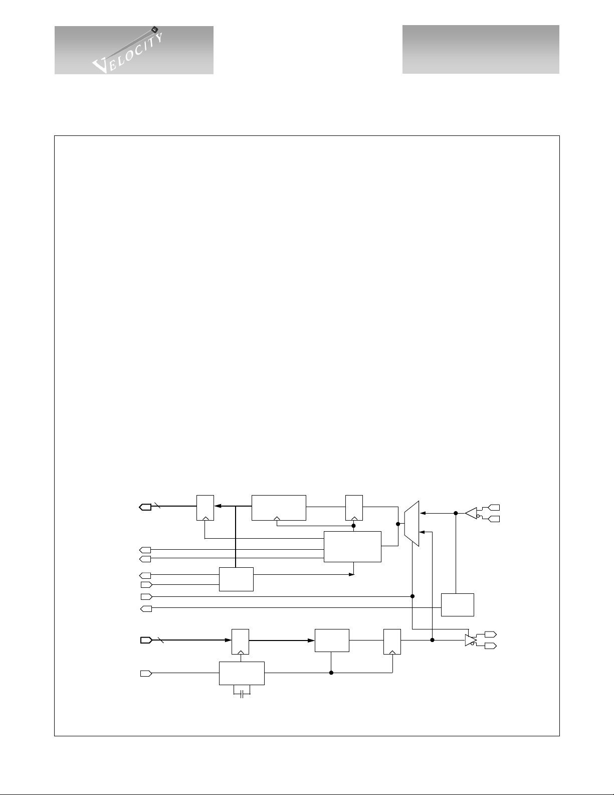
VSC7123 Block Diagram
R(0:9)
RCLK
RCLKN
COMDET
ENCDET
EWRAP
SIGDET
T(0:9)
REFCLK
G52212-0, Rev 4.3 Page 1
03/25//01
10
10
© VITESSE SEMICONDUCTOR CORPORATION • 741 Calle Plano • Camarillo, CA 93012
Q D
Comma
Detect
x10 Clock
Multiply
Tel: (800) VITESSE • FAX: (805) 987-5896 • Email: prodinfo@vitesse.com
Serial to
QD
Parallel
÷10
÷20
Parallel
to Serial
Internet: www.vitesse.com
Q D
Clock
Recovery
2:1
Signal
Detect
D QD Q
NOT SHOWN: JTAG Boundary Scan
RX+
RX-
TX+
TX-
Page 2
V
E
L
O
C
M
T
Y
T
I
VITESSE
SEMICONDUCTOR CORPORATION
10-Bit Transceiver for Fibre
Channel and Gigabit Ethernet
Data Sheet
VSC7123
Functional Description
Clock Synthesizer
The VSC7123 clock synthesizer multiplies the reference frequency provided on the REFCLK pin by 10 to
achieve a baud rate clock between 0.98GHz and 1.36GHz. The on-chip Phase Lock Loop (PLL) uses a single
external 0.1
Serializer
The VSC7123 accepts TTL input data as a parallel 10-bit character on the T(0:9) bus, which is latched into
the input register on the rising edge of REFCLK. This data is serialized and transmitted on the TX PECL
differential outputs at a bau d rate that is 10 ti mes the frequenc y of the REFCLK , with bit T0 tra nsmitted first.
User data should be encoded using 8B/10B block code or equivalent.
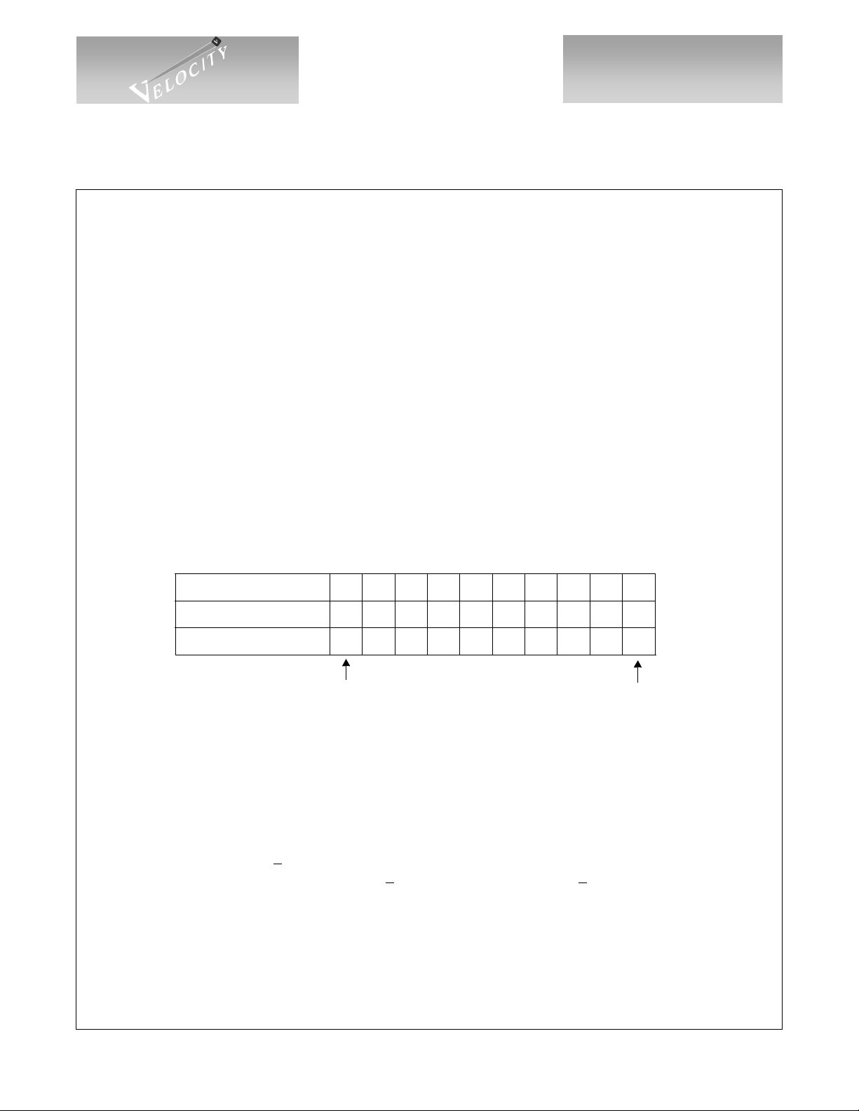
Transmission Character Interface
An encoded byte is 10 bits and is referred to as a transmission character. The 10 bit interface on the
VSC7123 corresponds to a transmission character. This mapping is illustrated in Figure 1.
µF capacitor to control the Loop Filter.
Figure 1: Transmission Order and Mapping of an 8B/10B Character
Parallel Data Bits
8B/10B Bit Position
Comma Character
Last Data Bit Transmitted
Clock Recovery
The VSC7123 accepts differential high-speed serial inputs on the RX+/RX- pins, extracts the clock and
retimes the data. Equalizers are included in the receiver to open the data eye and compensate for InterSymbol
Interference which may be present in the incoming data. The serial bit stream should be encoded to provide DC
balance and limited run length by an 8B/10B encoding scheme. The Clock Recovery Unit is completely
monolithic an d requires no ex ternal componen ts. For proper ope ration, the baud ra te of the data stream to be
recovered should be within +
systems would use 125MHz oscillators with a +
pairs.
Deserializer
The recovered serial bit stream is converted into a 10-bit parallel output character. The VSC7123 provides
complementary TTL recovered clocks, RCLK and RCLKN, which are 1/20
are generated by dividing down the high-speed recovered clock, which is phase-locked to the serial data. The
200 ppm of 10 times the REFCLK frequency. For example, Gigabit Ethernet
T9 T8 T7 T6 T5 T4 T3 T2 T1 T0
j
hgf iedcba
XXX1111100
First Data Bit Transmitted
100ppm accuracy resulting in +200 ppm between VSC7123
th
of the serial baud rate. The clocks
Page 2 G52212-0, Rev 4.3
© VITESSE SEMICONDUCTOR CORPORATION • 741 Ca l le Pl an o • Camarillo, CA 93012
Tel: (800) VITESSE • FAX: (805) 987-5896 • Email: prodinfo@vitesse.com
Internet: www.vitesse.com
03/25/01
Page 3

V
E
L
O
C
M
T
Y
T
I
VITESSE
SEMICONDUCTOR CORPORATION
Data Sheet
VSC7123
serial data is retimed, deserialized and output on R(0:9). The parallel data will be captured by the adjoining
protocol logic on the rising edges of RCLK and RCLKN.
If serial input data is not present or does not meet the required baud rate, the VSC7123 will continue to
produce a recovered clock, allowing downstream logic functionality to continue. Under these circumstances,
the RCLK/RCLKN output frequency differ from its expected frequency by no more than +
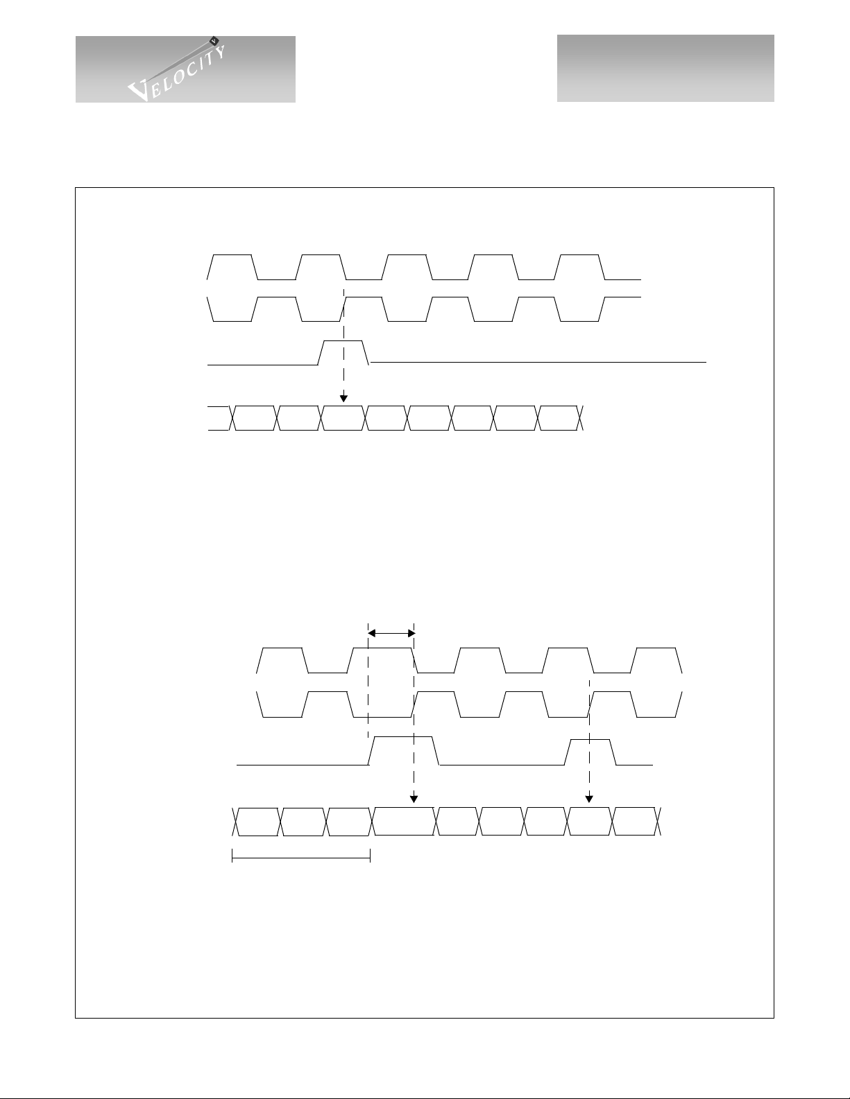
Word Alignment
The VSC7123 provides 7-bit comma character recognition and data word al ig nment . Word synchr oni zat ion
is enabled by asserting ENCDET HIGH. When synchronization is enabled, t he recei ve r exami nes the recov ered
serial data for the presence of the “Comma” character. This pattern is “0011111XXX”, where the leading zero
corresponds to the first bit received. The comma sequence is not contained in any normal 8B/10B coded data
character or pair of adjacent characters. It occurs only within special characters, known as K28.1, K28.5 and
K28.7, which are defined for synchronization purposes. Improper alignment of the comma character is defined
as any of the following conditions:
1) The comma is not aligned within the 10-bit transmission character such that R0...R6 = “0011111.”
2) The comma straddles the boundary between two 10-bit transmission characters.
3) The comma is properly aligned but occurs in the received character presented during the rising edge of
RCLK rather than RCLKN.
When ENCDET is HIGH and an improperly aligned comma is encountered, the recovered clock is
stretched (never slivered) so that the comma character and recovered clocks are properly aligned to R(0:9). This
results in proper character and word alignment. When the parallel data alignment changes in response to a
improperly aligned comma p a tter n, some data which would have been present ed o n t he par al le l output port may
be lost. Additionally, the first Comma pattern may also be lost or corrupted. Subsequent data will be output
correctly and properly aligned. When ENCDET is LOW, the current alignment of the serial data is maintained
indefinitely, regardless of data pattern.
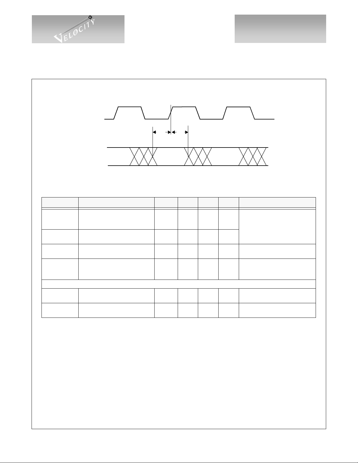
When encountering a comma character, COMDET is driven HIGH. The COMDET pulse is presented
simultaneously with the comma character and has a duration equal to the data, or half of an RCLK period. The
COMDET signal is timed such that it can be captured by the adjoining protocol logic on the rising edge of
RCLKN. Functional waveforms for syn chr oni zati on are given in Figure 2 and F ig ure 3 . Fig ure 2 shows the case
when a comma character is detected and no phase adjustment is necessary. Figure 2 illustrates the position of
the COMDET pulse in relation to the comma character on R(0:9). Figure 3 shows the case where the K28.5 is
detected, but it is misaligned so a change in the output data alignment is required. Note that up to three
characters prior to the comma character may be corrupted by the realignment process.
10-Bit Transceiver for Fibre
Channel and Gigabit Eth er net
1%.
G52212-0, Rev 4.3 Page 3
03/25//01
© VITESSE SEMICONDUCTOR CORPORATION • 741 Calle Plano • Camarillo, CA 93012
Tel: (800) VITESSE • FAX: (805) 987-5896 • Email: prodinfo@vitesse.com
Internet: www.vitesse.com
Page 4
V
E
L
O
C
M
T
Y
T
I
VITESSE
SEMICONDUCTOR CORPORATION
10-Bit Transceiver for Fibre
Channel and Gigabit Ethernet
Figure 2: Detection of a Properly Aligned Comma Character
RCLK
RCLKN
COMDET
R(0:9)
Data Sheet
VSC7123
K28.5 TChar TChar TChar
TChar: 10-bit transmission character
Figure 3: Detection
RCLK
RCLKN
COMDET
R(0:9)
Receiving Two Consecutive K28.5+TChar Transmission Words
Clock Stretching
K28.5 TChar T Char TChar K28.5 TChar
Potentially Corrupted
TChar: 10-bit transmission character
Page 4 G52212-0, Rev 4.3
© VITESSE SEMICONDUCTOR CORPORATION • 741 Ca l le Pl an o • Camarillo, CA 93012
Tel: (800) VITESSE • FAX: (805) 987-5896 • Email: prodinfo@vitesse.com
Internet: www.vitesse.com
03/25/01
Page 5
V
E
L
O
C
M
T
Y
T
I
VITESSE
SEMICONDUCTOR CORPORATION
Data Sheet
VSC7123
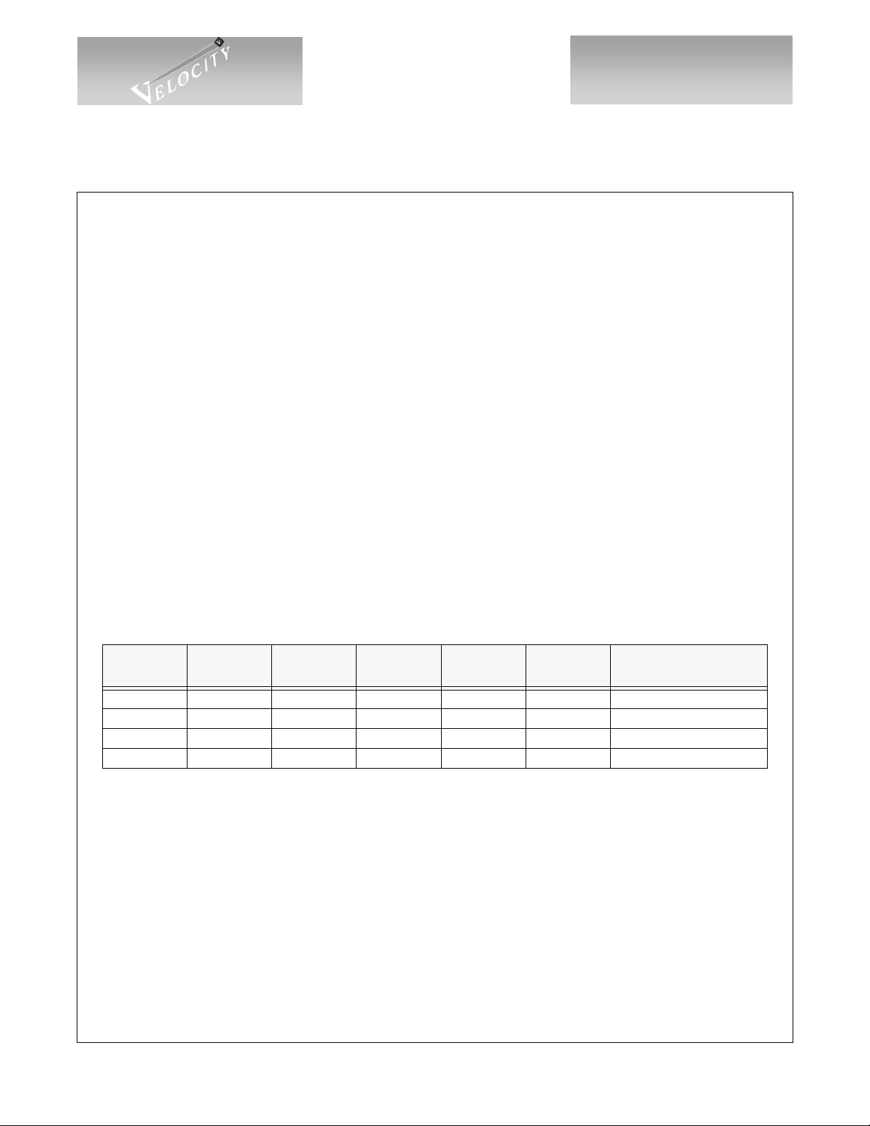
Signal Detection
The receiver has an output, SIGDET, indicating, when HIGH, that the RX input contains a valid Fibre
Channel or Gigabit Ethernet signal. A combination of one analog and three digital checks are used to determi ne
if the incoming signal contains valid data. SIGDET is updated every four RCLKs. If during the current period,
all the four criteria are met, SIGDET will be HIGH during th e next 4 RCLK perio d. If during t he current per iod,
any of the four criteria is not met, SIGDET will be LOW during the next 4 RCLK period.
1) Analog transition detection is performed on the input to verify that the signal swings are of adequate
amplitude. The RX+/- input buffer contains a differential voltage comparator which will go HIGH if the
differential peak-to-peak amplitude is greater than 400mV or LOW if under 200mV. If the amplitude is
between 200mV and 400mV, the output is indeterminate.
2) Data on R(0:9) is monitored for all zeros (0000000000). If this pattern is encountered during the current
RCLK interval, the SIGDET output will go LOW during the next four RCLK interval.
3) Data on R(0:9) is monitored for all ones (1111111111). If this pattern is encountered during the current
RCLK interval, the SIGDET output will go LOW during the next four RCLK interval.
4) Data on R(0:9) is monitored for K28.5- (0011111010). Unlike previous patterns, the interval during which
a K28.5- must occur is 64K+24 10-bit characters in length. Valid Fibre Channel or Gigabit Ethernet data
will contain a K28.5- character during any period of this length. If a K28.5- is not detected during the
monitoring period, SIGDET will go LOW during the next period.
The behavior of SIGDET is affected by EWRAP and ENCDET as shown in Table 1.
10-Bit Transceiver for Fibre
Channel and Gigabit Eth er net
Table 1: Signal Detect Behavio r
EWRAP ENCDET COMDET
0 0 Disabled Enabled Enabled Enabled Normal
0 1 Enabled Enabled Enabled Disabled SIGDET ignores commas
1 0 Disabled Enabled Disabled Disabled Rollback
1 1 Enabled Enabled Disabled Disabled Loopback
Note: COMDET, RCLK, RCLKN and R(0:9) are unaltered by SIGDET.
JT AG Access Port
A JTAG Access Port is provided to assist in board-level testing. Through this port, most pins can be
accessed or controlled and all TTL outputs can be tri-stated. A full description of the JTAG functions on this
device is available in “VSC7123/VSC7133 JTAG Access Port Functionality.”
Transition
Detect
All Zeros/
All Ones
K28.5
Presence
Mode
G52212-0, Rev 4.3 Page 5
03/25//01
© VITESSE SEMICONDUCTOR CORPORATION • 741 Calle Plano • Camarillo, CA 93012
Tel: (800) VITESSE • FAX: (805) 987-5896 • Email: prodinfo@vitesse.com
Internet: www.vitesse.com
Page 6
V
E
L
O
C
M
T
Y
T
I
VITESSE
SEMICONDUCTOR CORPORATION
10-Bit Transceiver for Fibre
Channel and Gigabit Ethernet
Figure 4: Transmit Timing Waveforms
REFCLK
T
T(0:9)
Data Valid
T a ble 2: Transmit AC Characteristics
Parameters Description Min Typ Max Units Conditions
T
T
T
SDR,TSDF
T
LA T
1
2
T(0:9) Setup time to the rising
edge of REFCLK
T(0:9) hold time after the rising
edge of REFCLK
TX+/TX- rise and fall time ——300 ps
Latency from r ising edge of
REFCLK to T0 appearing on
TX+/TX-
Transmitter Output Jitter Allocation
RJ Random jitter (RMS) — 58ps.
DJ
Serial data output deterministic
jitter (pk-pk)
T
1
Data Valid
1.5 ——ns
1.0 ——ns
8bc —
2
Data Valid
8bc+
4ns
— 30 80 ps.
Measured between the valid data
level of T(0:9) to the 1.4V point
of REFCLK.
20% to 80%, 50Ω load to
-2.0.
V
DD
bc = Bit clocks
ns
ns = Nano second
Measured at SO+/-, 1 sigma
deviation of 50% cro s si ng poin t.
IEEE 802.3Z Clause 38.68,
tested on a sample basis.
Data Sheet
VSC7123
Page 6 G52212-0, Rev 4.3
© VITESSE SEMICONDUCTOR CORPORATION • 741 Ca l le Pl an o • Camarillo, CA 93012
Tel: (800) VITESSE • FAX: (805) 987-5896 • Email: prodinfo@vitesse.com
Internet: www.vitesse.com
03/25/01
Page 7

V
E
L
O
C
M
T
Y
T
I
VITESSE
SEMICONDUCTOR CORPORATION
Data Sheet
VSC7123
RCLK
RCLKN
R(0:9)
Table 3: Receive AC Characterist ics
Parameters Description Min. Max. Units Conditions
TTL Outputs Valid prior to
RCLK/RCLKN rise
TTL Outputs Valid after
RCLK or RCLKN rise
Delay betwee n rising edge of
RCLK to rising edge of
RCLKN
Period of RCLK and
RCLKN
R(0:9), COMDET, SIGDET,
RCLK and RCLKN rise and
fall time
Latency from RX to R (0:9) 12 bc + 1 ns 13 bc + 9 ns
Data acquisition lock time — 1400 bc
T
T
LOCK
T
1
T
2
T
3
T
4
, T
R
F
R
LA T
(1)
Figure 5: Receive Timing Waveforms
T
4
T
2
10 x T
+500
2.02 x
T
REFCLK
Data Valid
T
1
Data Valid Data Valid
4.0
3.0
3.0
2.0
10 x T
RX
-500
1.98 x
T
REFCLK
— 2.4 ns
—
—
—
—
RX
10-Bit Transceiver for Fibre
Channel and Gigabit Eth er net
T
3
At 1.0625Gb/s
ns
At 1.25Gb/s
At 1.0625Gb/s
ns
At 1.25Gb/s
is the bit period of the
T
ps
ps
bc
ns
RX
incoming data on Rx.
Whether or not l ocked to
serial data.
Between V
IH(MIN)
, into 10pf load.
V
bc = bit clo c k
ns = nano second
8B/10B IDLE pat tern.
bc = bit clocks
IL(MAX)
and
NOTE: (1) Probability of recovery for data acquisition is 95% per Section 5.3 of FC-PH rev. 4.3.
G52212-0, Rev 4.3 Page 7
03/25//01
© VITESSE SEMICONDUCTOR CORPORATION • 741 Calle Plano • Camarillo, CA 93012
Tel: (800) VITESSE • FAX: (805) 987-5896 • Email: prodinfo@vitesse.com
Internet: www.vitesse.com
Page 8

V
E
L
O
C
M
T
Y
T
I
VITESSE
SEMICONDUCTOR CORPORATION
10-Bit Transceiver for Fibre
Channel and Gigabit Ethernet
Figure 6: REFCLK Timing Waveforms
T
L
REFCLK
T
R
Table 4: Reference Clock Requirements
Parameter Description Min Max Units Conditions
FR Frequency Range 98 136 MHz
FO Frequency Offset -200 200 ppm
DC REFCLK duty cycle 35 65 % Measured at 1.5V
T
R,TF
REFCLK rise and fall time — 1.5 ns Between V
T
H
T
F
Range over which both transmit and
receive reference clocks on any link may
be centered.
Maximum frequency offs et between
transmit and receive reference cloc ks on
one link.
IL(MAX)
Data Sheet
VSC7123
V
IH(MIN)
V
IL(MAX)
and V
IH(MIN)
Page 8 G52212-0, Rev 4.3
© VITESSE SEMICONDUCTOR CORPORATION • 741 Ca l le Pl an o • Camarillo, CA 93012
Tel: (800) VITESSE • FAX: (805) 987-5896 • Email: prodinfo@vitesse.com
Internet: www.vitesse.com
03/25/01
Page 9

V
E
L
O
C
M
T
Y
T
I
VITESSE
SEMICONDUCTOR CORPORATION
Data Sheet
VSC7123
10-Bit Transceiver for Fibre
Channel and Gigabit Eth er net
Figure 7: Parametric Measurement Information
Serial Input Rise and Fall Time TTL Input and Output Rise and Fall Time
80%
20%
T
R
T
F
Receiver Input Eye Diagram Jitter Tolerance Mask
Bit Time
Amplitude
T
R
T
F
V
IH(MIN)
V
IL(MIN)
Serial Output Load
Z0 = 75W
V
DD
24% Minimum Eye Width%
Parametric Test Load Circuit
50 or 75W
– 2.0V
TTL AC Output Load
10pF
G52212-0, Rev 4.3 Page 9
03/25//01
© VITESSE SEMICONDUCTOR CORPORATION • 741 Calle Plano • Camarillo, CA 93012
Tel: (800) VITESSE • FAX: (805) 987-5896 • Email: prodinfo@vitesse.com
Internet: www.vitesse.com
Page 10

V
E
L
O
C
M
T
Y
T
I
VITESSE
SEMICONDUCTOR CORPORATION
10-Bit Transceiver for Fibre
Channel and Gigabit Ethernet
V
DDD
INPUT
GND
TTL Inputs (not REFCLK)
V
DD
+3.3 V
Figure 8: Input Structures
INPUT
INPUT
V
DDD
3K
4K
3K
4K
GND
High-Speed Input (RX+/RX-)
Data Sheet
VSC7123
REFCLK
12.6K
9.3K
12.6K
GND
REFCLK TTL Input
V
DDT
V
SST
TTL Outputs
V
SSD
9.3K
OUTPUT
GND
V
DDD
V
DDP
High-Speed Outputs (TX+/-)
TX+
TX-
Page 10 G52212-0, Rev 4.3
© VITESSE SEMICONDUCTOR CORPORATION • 741 Ca l le Pl an o • Camarillo, CA 93012
Tel: (800) VITESSE • FAX: (805) 987-5896 • Email: prodinfo@vitesse.com
Internet: www.vitesse.com
03/25/01
Page 11

V
E
L
O
C
M
T
Y
T
I
VITESSE
SEMICONDUCTOR CORPORATION
Data Sheet
VSC7123
10-Bit Transceiver for Fibre
Channel and Gigabit Eth er net
DC Characteristics (over recommend ed ope rati ng con di tion s)
Parameters Description Min Typ Max Units Conditions
2.4 —— V
——0.5 V
2.0 — 5.5 V
0 — 0.8 V
— 50 500 µA
——-500 µA
1200 — 2200 mVp-p
1000 — 2200 mVp-p
300 — 2600 mVp-p
3.14 — 3.47 V
— 650 900 mW
— 190 260 mA
——100 mA
IOH = –1.0 mA
IOL = +1.0 mA
5V Tolerant Inputs
—
VIN = 2.4V
VIN = 0.5V
75Ω to VDD – 2.0V
(TX+) - (TX-)
50Ω to VDD – 2.0V
(TX+) - (TX-)
Internally biased to VDD/2
(RX+) - (RX-)
3.3V±5%
Outputs open,
V
DD
Outputs open, Case temp =
o
95
V
DDA
∆V
∆V
V
V
V
V
I
I
OUT75
OUT50
∆V
V
P
I
DD
I
DDA
OH
OL
IH
IL
IH
IL
IN
DD
D
(1)
Output HIGH voltage (TTL)
Output LOW voltage (TTL)
Input HIGH voltage (TTL)
Input LOW voltage (TTL)
Input HIGH current (TTL)
Input LOW current (TTL)
TX output differential peak-
(1)
to-peak voltage swing
TX output differential peak-
(1)
to-peak voltage swing
RX Input differential peak-
to-peak input sensitivity
Supply voltage
Power dissipation
Supply current (all supplies)
Analog suppl y current
= VDD max
C, VDD = VDD max
= V
DDA
max
NOTE: (1) Refer to Application Note, AN-37, for differential measurement techniques.
G52212-0, Rev 4.3 Page 11
03/25//01
© VITESSE SEMICONDUCTOR CORPORATION • 741 Calle Plano • Camarillo, CA 93012
Tel: (800) VITESSE • FAX: (805) 987-5896 • Email: prodinfo@vitesse.com
Internet: www.vitesse.com
Page 12

V
E
L
O
C
M
T
Y
T
I
VITESSE
SEMICONDUCTOR CORPORATION
10-Bit Transceiver for Fibre
Channel and Gigabit Ethernet
Absolute Maximum Ratings
Power Supply Voltage, (VDD) ................................................................................................................ –0.5V to +4V
DC Input Voltage (PECL inputs)
DC Input Voltage (TTL inputs)
DC Output Voltage (TTL outputs)
Output Current (TTL outputs).................................................................................................................... +
Output Current (PECL outputs)...................................................................................................................+50mA
Case Temperature Under Bias
Storage Temperature
.......................................................................................................................... –65
................................................................................................ –0.5V to V
........................................................................................................... –0.5V to +5.5V
............................................................................................ –0.5V to V
.......................................................................................................... –55
(1)
Data Sheet
VSC7123
o
C to +125oC
o
C to +150oC
Recommended Operating Conditions
Power Supply Voltage, (VDD)................................................................................................................+3.3V+5%
o
Operating Temperature Range ............................................................. 0
Note: (1) CAUTION: Stresses listed under “Absolute Maximum Ratings” may be applied to devices one at a time without causing
permanent damage. Functionality at or above the values listed is not implied. Exposure to these values for extended periods may affect device reliability.
C Ambient to +95oC Case Temperature
DD
+ 0.5V
DD
+0.5V
50mA
ESD Ratings
Proper ESD procedures should be used when handling this product. The VSC7123 is rated to the following
ESD voltages based on the human body and charge device models:
1. All pins are rated at or above 1000V (charge device model).
2. All pins are rated at or above 2000V (human body model).
Page 12 G52212-0, Rev 4.3
© VITESSE SEMICONDUCTOR CORPORATION • 741 Ca l le Pl an o • Camarillo, CA 93012
Tel: (800) VITESSE • FAX: (805) 987-5896 • Email: prodinfo@vitesse.com
Internet: www.vitesse.com
03/25/01
Page 13

V
E
L
O
C
M
T
Y
T
I
VITESSE
SEMICONDUCTOR CORPORATION
Data Sheet
VSC7123
Package Pin Descriptions
V
SSD
T0
T1
T2
V
DDD
T3
T4
T5
T6
V
DDD
T7
T8
T9
V
SSD
V
SSA
CAP0
1
3
5
7
9
11
13
15
Figure 9: Pin Diagram
(Top View)
SSD
DDP
V
V
63 61 59 57 55 53 51 49
DDP
DDDVSSD
DDD
V
TX+
V
TX-
TRSTN
TMS
V
RX+
N/C
SSDVDDD
V
RX-
VSC7123
17 19 21 23 25 27 29 31
10-Bit Transceiver for Fibre
Channel and Gigabit Eth er net
TCK
TDI
47
45
43
41
39
37
35
33
COMDET
V
SST
R0
R1
R2
V
DDT
R3
R4
R5
R6
V
DDT
R7
R8
R9
V
SST
CAP1
DDD
V
SSD
V
V
REFCLK
DDA
V
EWRAP
DDD
ENCDET
SSD
V
SIGDET
DDT
DDD
TDO
V
V
RCLKN
SST
V
RCLK
Table 5: Pin Identifications
Pin # Name Description
2,3,4,6
7,8,9,11
12,13
22 REFCLK
G52212-0, Rev 4.3 Page 13
03/25//01
T0,T1,T2,T3
T4,T5,T6,T7
T8,T9
INPUTS - TTL:
10-bit transmit character. Parallel data on this bus is clocked in on the rising edge of
REFCLK. The data bit corresponding to T0 is transmitted first.
INPUT - TTL:
This rising edge of this clock latches T(0:9) into the input register. It also provides the
reference clock, at one tenth the baud rate to the PLL.
© VITESSE SEMICONDUCTOR CORPORATION • 741 Calle Plano • Camarillo, CA 93012
Tel: (800) VITESSE • FAX: (805) 987-5896 • Email: prodinfo@vitesse.com
Internet: www.vitesse.com
Page 14

V
E
L
O
C
M
T
Y
T
I
VITESSE
SEMICONDUCTOR CORPORATION
10-Bit Transceiver for Fibre
Channel and Gigabit Ethernet
Pin # Name Description
OUTPUTS - Differential PECL (AC-coupling recommended):
62, 61 TX+, TX-
45,44,43,41
40,39,38,36
35,34
19 EWRAP
54, 52 RX+, RX-
31, 30
24 ENCDET
47 COMDET
26 SIGDET
16, 17 CAP0, CAP1 ANALOG: Differential capacitor for the CMU’s VCO, 0.1 µF nominal.
49 TCK INPUT - TTL: JT AG clock inpu t. Not no rmally conn ecte d .
48 TDI INPUT - TTL: JTAG data input. Not normally connected.
55 TMS INPUT - TTL: JTAG mode select input. Normally tied to V
56 TRSTN INPUT - TLL: JTAG reset input. Tie to V
27 TDO OUTPU - TTL: JTAG data output. Normally tri-stated.
18 VDDA Analog Power Supply
15 VSSA Analog Ground
5,10,20,23
28,50,57,59
1,14,21,25
51,58,64
29, 37, 42 VDDT TTL Output Power Supply
32, 33, 46 VSST TTL Output Ground
60,63 VDDP PECL I/O Power Supply
53 N/C No internal connection
R0,R1,R2,R3
R4,R5,R6,R7
R8,R9
RCLK,
RCLKN
VDDD Digital Logic Power Supply
VSSD Digital Logic Ground
These pins output the serialized transmit data when EWRAP is LOW. When EWRAP is
HIGH, TX+ is HIGH and TX- is LOW.
OUTPUTS - TTL:
10-bit received character. Parallel data on this bus is clocked out on the rising edges of
RCLK and RCLKN. R0 is the first bit received on RX+/RX-.
INPUT - TTL:
LOW for normal operation. When HIGH, an internal loopback path from the transmitter to
the receiver is enabled. TX+ is held HIGH and TX- is held LOW.
INPUTS - Differential PECL (AC-coupling recommended):
The serial receive data inputs selected when EWRAP is LOW. Internally biased to VDD/2,
with 3.3KΩ resistors from each input pin to VDD and GND.
OUTPUT - Complementary TTL:
Recovered clocks derived from 1/20
RCLK or RCLKN corresponds to a new word on R(0:9).
INPUT - TTL:
Enables COMDET and word resynchron iz ation when HIGH. When LOW, keeps current
word alignment and disables COMDET.
OUTPUT - TTL:
This output goes HIGH for half of an RCLK period to indicate that R(0:9) contains a comma
character (‘0011111XXX’). COMDET will go HIGH only during a cycle when RCLKN is
rising. COMDET is enabled by ENCDET being HIGH.
OUTPUT - TTL
SIGnal DETect. This output goes HIGH when the RX input contains a valid Fibre Channel or
Gigabit Ethernet signal. A LOW indicates an invalid signal.
Data Sheet
VSC7123
th
of the RX+/- data stream. Each rising transition of
DDD
for normal operation.
SSD
Page 14 G52212-0, Rev 4.3
© VITESSE SEMICONDUCTOR CORPORATION • 741 Ca l le Pl an o • Camarillo, CA 93012
Tel: (800) VITESSE • FAX: (805) 987-5896 • Email: prodinfo@vitesse.com
Internet: www.vitesse.com
03/25/01
Page 15
V
E
L
O
C
M
T
Y
T
I
VITESSE
SEMICONDUCTOR CORPORATION
Data Sheet
VSC7123
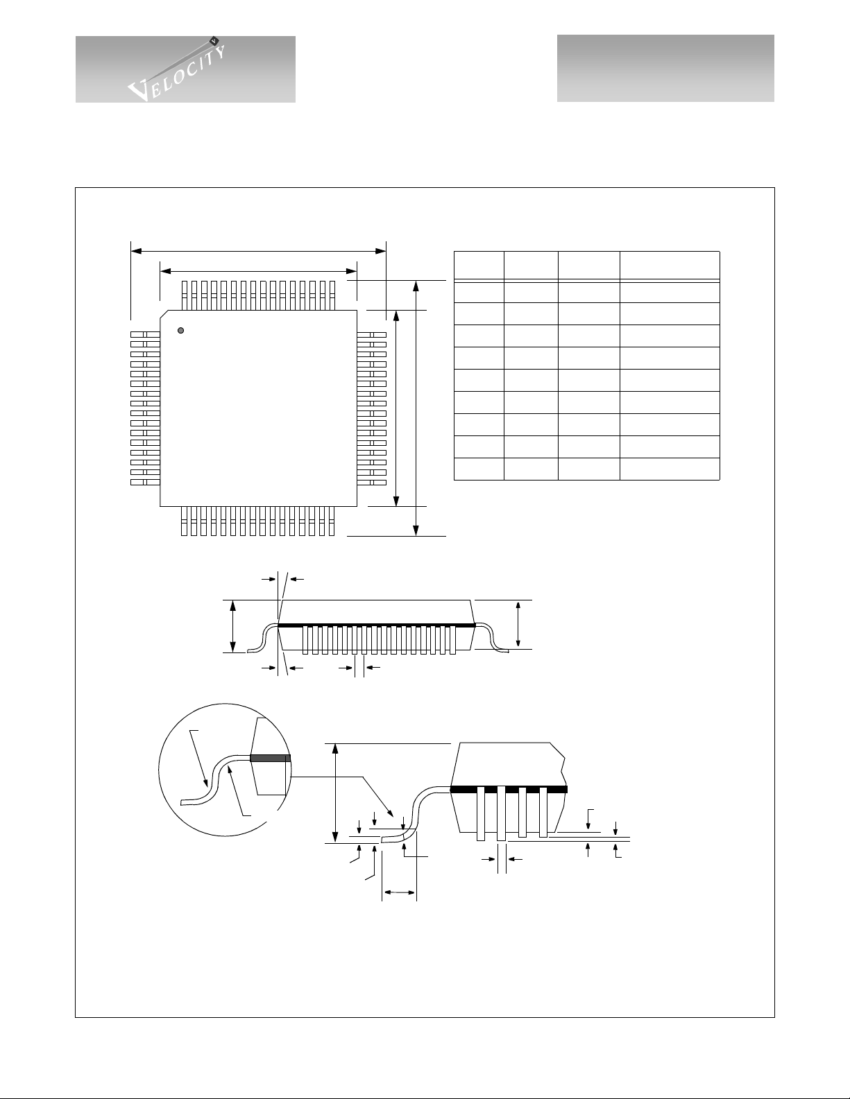
Package Information: 64-pin PQFP
F
G
64 49
1
16
3217
10o TYP
48
33
IH
10-Bit Transceiver for Fibre
Channel and Gigabit Eth er net
Item 10mm 14mm Tolerance
A2.452.35 MAX
A2 2.00 2.00 +0.10/-0.05
E0.220.35 ±0.05
F 13.20 17.20 ±0.25
G 10.00 14.00 ±0.10
H 13.20 17.20 ±0.25
I 10.00 14.00 ±0.10
J 0.88 0.88 +0.15/-0.10
K0.500.80 BASIC
A
0.30 RAD. TYP.
100 TYP
0.20 RAD. TYP.
0.17 MAX.
A2
K
A
0o- 8o
0.25
J
E
NOTES:
Drawing not to scale.
All units in mm unless otherwise noted.
STANDOFF
0.25 MAX.
0.102 MAX. LEAD
COPLANARITY
G52212-0, Rev 4.3 Page 15
03/25//01
© VITESSE SEMICONDUCTOR CORPORATION • 741 Calle Plano • Camarillo, CA 93012
Tel: (800) VITESSE • FAX: (805) 987-5896 • Email: prodinfo@vitesse.com
Internet: www.vitesse.com
Page 16

V
E
L
O
C
M
T
Y
T
I
VITESSE
SEMICONDUCTOR CORPORATION
10-Bit Transceiver for Fibre
Channel and Gigabit Ethernet
Package Information: 64-pin TQFP
F
G
64 49
1
L
M
16
3217
11/13o 8 PLACES
48
33
IH
Data Sheet
VSC7123
Item 10 mm Tolerance
A1.20 MAX
A1 0.10 ±0.05
A2 1.00 ±0.05
E 0.22 ±0.05
F 12.00 BASIC
G 10.00 BASIC
H 12.00 BASIC
I 10.00 BASIC
J 0.60 ±0.15
K0.50 BASIC
L3.80 BASIC
M3.80 BASIC
A
0.08/0.20 R
0.08 R MIN
0.09/0.20
A2
K
A
0o- 7o
0.25
J
E
NOTES:
Drawing not to scale.
All units in mm unless otherwise noted.
ST ANDOFF
A1
0.08 MAX. LEAD
COPLANARITY
Page 16 G52212-0, Rev 4.3
© VITESSE SEMICONDUCTOR CORPORATION • 741 Ca l le Pl an o • Camarillo, CA 93012
Tel: (800) VITESSE • FAX: (805) 987-5896 • Email: prodinfo@vitesse.com
Internet: www.vitesse.com
03/25/01
Page 17

V
E
L
O
C
M
T
Y
T
I
VITESSE
SEMICONDUCTOR CORPORATION
Data Sheet
VSC7123
10-Bit Transceiver for Fibre
Channel and Gigabit Eth er net
Package Thermal Considerations
The VSC7123 is packaged in a 14mm, thermally-enhanced PQFP with an internal heat spreader a 10 mm,
thermally enhanced PQFP and a 10mm cavity-down, exposed pad TQFP. These packages use industry-standard
EIAJ footprints, but have been enhanced to improve thermal dissipation. The construction of the packages is
shown in Figure 10.
Figure 10: PQFP Package Cross Section
Plastic Molding Compound
Lead
T a ble 6: Thermal Resistance
Bond Wire
Internal Heat Spreader
Insulator
Die
Symbol Description
θ
jc
θ
ca
θ
ca-100
θ
ca-200
θ
ca-400
θ
ca-600
Thermal resistance from junction-to-case 10 9.5 7.0
Thermal resistance from case-to-ambient in still air including
conduction t hrough the leads.
Thermal resistance from case-to-ambien t with 100 LFM airflow 41 26 38
Thermal resistance from case-to-ambient with 200 LFM airflow 37 24 35
Thermal resistance from case-to-ambien t with 400 LFM airflow 32 21 33
Thermal resistance from case-to-ambien t with 600 LFM airflow 28 18 30
10mm
PQFP
50 29 40
14mm
PQFP
10mm
TQFP
Units
o
C/W
o
C/W
o
C/W
o
C/W
o
C/W
o
C/W
The VSC7123 is designed to operate with a case temperature up to 95oC. The user must guarantee that the
case temperature specification is not violated. With the thermal resistances shown in Table 7, the 10mm
thermally-enhanced PQFP package can operate in still air ambient te mperatures of 50
50 C/W]. The 14mm th ermally-enh anced PQFP pack age can operate in still air amb ient temperatur es of 69
o
[69
C = 95oC - 0.9W * 29 C/W]. The TQFP package can operate in a still air ambient temperature of 59oC
o
[59
C = 95oC - 0.9W * 40 C/W]. If the ambient air temperature exceeds these limits, a form of cooling through
o
C [50oC = 95oC - 0.9W *
o
a heatsink or an increase in airflow must be provided.
Moisture Sensitivity Level
This device is rated at a Moisture Sensitivity Level 3 rating with maximum floor life of 168 hours at 30ºC,
60% relative humidity. Please refer to Application Note AN-20 for appropriate handling procedures.
C
G52212-0, Rev 4.3 Page 17
03/25//01
© VITESSE SEMICONDUCTOR CORPORATION • 741 Calle Plano • Camarillo, CA 93012
Tel: (800) VITESSE • FAX: (805) 987-5896 • Email: prodinfo@vitesse.com
Internet: www.vitesse.com
Page 18

V
E
L
O
C
M
T
Y
T
I
VITESSE
SEMICONDUCTOR CORPORATION
10-Bit Transceiver for Fibre
Channel and Gigabit Ethernet
Ordering Informatio n
The part number for this product is formed by a combination of the device number and the package style.
Device Type
10-Bit Transc eiv er
Marking Information
The package is marked with three lines of text as shown in Figure 11 (QU package shown).
VSC7123
Data Sheet
VSC7123
xx
Package
QN: 64-Pin, 14x14mm PQFP
QU: 64-Pin, 10x10mm PQFP
RD: 64-Pin, 10x10mm TQFP
Figure 11: Package Marking Information
Pin 1 Identifier
Part Number
DateCode
Notice
Vitesse Semiconductor Corporation (“Vitesse”) provides this docume nt for informational purpo s es only. All information in this docume nt, including descriptions of features, functions, performance, technical specifications and availability, is subject to change without notice at any time. Nothing contained in this document shall be co nstrued as extend ing any warra nty or promise, express or implie d, that any Vitesse product will be
available as described or will be suitable for or will accomplish any partic ul ar task.
Vitesse products are not intended for use in life support applia nc es, devices or systems. Use of a Vitesse product in such applications without written consent is prohibited.
VSC7123QU
####AAAAA
VITESSE
Package Suffi x
Lot Tracking Code (4 or 5 characters)
Page 18 G52212-0, Rev 4.3
© VITESSE SEMICONDUCTOR CORPORATION • 741 Ca l le Pl an o • Camarillo, CA 93012
Tel: (800) VITESSE • FAX: (805) 987-5896 • Email: prodinfo@vitesse.com
Internet: www.vitesse.com
03/25/01
 Loading...