

Page 1
VITESSE SEMICONDUCTOR CORPORATION
Page 1
4/10/00 741 Calle Plano, Camarillo, CA 93012 • 805/388-3700 • FAX: 805/987-5896
VITESSE
SEMICONDUCTOR CORPORATION
A
dvance Product Information
VSC6501
and Cable Driver at 1.485 Gb/s
SMPTE-292M Reclocker
G52310-0, Rev. 2.0
Draft Copy
Features
General Description
The VSC6501 is a SMPTE-292M compatible Reclocker with 2 or 4 user configurablable 75 ohm Cable
Driver outputs which operate at 1.485Gb/s. HDTV serial data on the SDI/SDI
inputs is recovered and retrans-
mitted on the SDO0/SDO0
and SDO1/SDO1 outputs. The CRU portion of the reclocker may be bypassed for
operation with non-HDTV data rates. The VSC6501 can be used to build routing switchers and video distribution amplifiers.
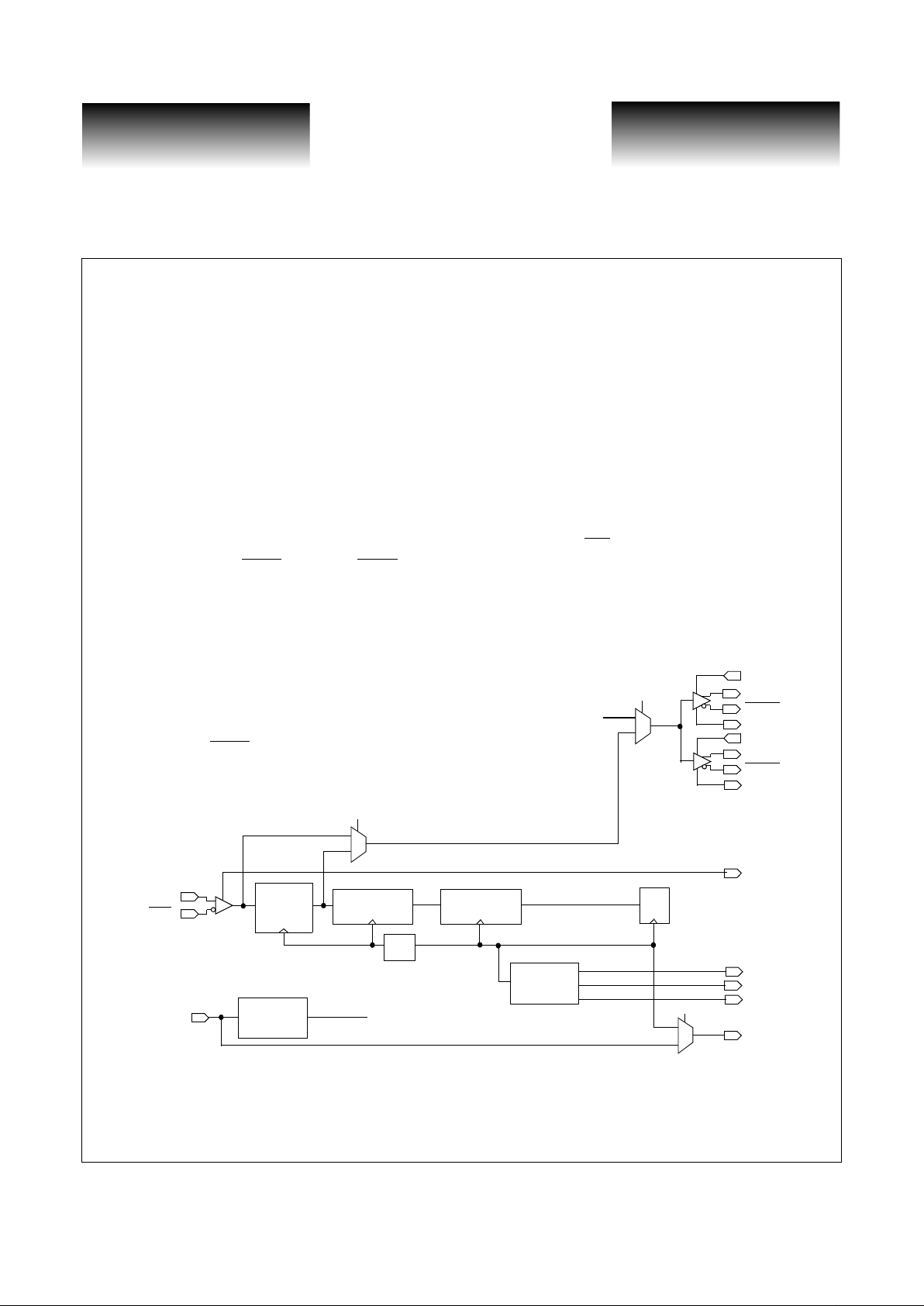
VSC6501 Reclocker Block Diagram
• Compliant with SMPTE-292M @ 1.485Gb/s
• Clock and Data Recovery
• 2 or 4 user Configurable 75 ohm cable driver
outputs
• CRU BYPASS mode for SMPTE 259M or
other data rates
• Buffered REFCLK output for distribution to
additional devices
• 3.3V, Low Power -- 800 mW typical
• 64-pin, 10x10x1.0mm Exposed Pad TQFP
LINE
FRAME
HANC
SDI
SDI
Clock/
Recovery
REFCLK
Clock
Multiply
1.485 GHz
74.25 MHz
x20
RCLK
1.485 GHz
BYP A SS
SDO0
SDO0
SIGDET
OE1
/20
ISET0
SDO1
SDO1
ISET1
Unit
*
CABLE DRIVER
OUTPUTS
DescramblerDeserializer
D Q
OE0
Framer
*
Page 2

VITESSE
SEMICONDUCTOR CORPORATION
Advance Product Information
VSC6501
Cable Driver at 1.485 Gb/s
SMPTE-292M Reclocker and
Page 2
VITESSE
SEMICONDUCTOR CORPORATION
741 Calle Plano, Camarillo, CA 93012 • 805/388-3700 • FAX: 805/987-5896 4/10/00
G52310-0, Rev. 2.0
Draft Copy
Reclocker Functional Description
Clock Multiplier Unit (CMU)
The CMU generates the internal 1.485 GHz baud rate clock from the 74.25 MHz TTL REFCLK input. The
rising edges of the REFCLK are used by a PLL which multiplies the frequency by a factor of 20. An off-chip
0.1uF capacitor sets the loop bandwidth of the CMU. REFCLK should be a high quality, low jitter signal with
sharp rise times in order t o mini mi ze the amount of jitter tr ansf err ed f r om the REFCLK through the CMU to t he
serializer. Although not shown on the block diagram, the digital CRU requires the baud rate clock of the CMU
for proper operation.
REFCLK is also buffered onto the RCLK output allowing multiple devices to be daisy-chained in order to
simplify REFCLK distribution to an array of devices.
Serial Input
The differential PE CL-sty le i np ut , SDI/S DI, is t he i np ut source f or 1.485 Gb/s SMPTE 292M data. An analog signal detector monitors the input signal for valid amplitude and outputs status on the SIGDET pin. If SIGDET is HIGH, the differential input swing is greater than 400 mV. If SIGDET is LOW, the differential swing is
below 200 mV. If the input swing is between 200 and 400 mV, the SIGDET output is indeterminate. The SIGDET function is disabled in Serializer mode and will output a LOW.
Clock Recovery Unit
The serial data on the SDI /SDI inpu t is sent to the digital Clock Recovery Unit (CRU) which extracts the
clock and retimes the data. This dig ital CRU is completely monol ithic and re quires no external comp onents.
Furthermore, it automaticall y locks ont o dat a when present and lo cks to REFCLK when data i s not presen t. This
eliminates the need for the system to control the CRU.
Descrambler and NRZI Decoder
The VSC6501 contains a descrambler whic h processes the recovered serial data and outputs u nscrambled
serial data from the deserialize r. The serial scrambled data is descrambled/NRZ I decoded assu ming data ha s
NRZI encoded with the following combined generator polynomial: G(x)=(x
9+x4
+1)(x+1). Descrambling is
enabled with the SCREN input is HIGH and disabled when LOW.
Pattern Detector
The VSC6501 monitors the serial data stream for SAV/EAV characters. These characters should be located
within each line of video data. If SAV/EAV is not det ect ed wi th in t he p eriod of one l in e, th e Framer send s a signal to the Deserializer to shift the data one bit. The Frame then looks for SAV/EAV and the process repeats until
properly detected. Without these patterns, serial data is not aligned in a ny way with the parallel outputs. The
Framer outputs a once-per-line (LINE) and a once-per-frame (FRAME) signal indicating the detection of the
proper synchronization pulse in the data.
Page 3
VITESSE SEMICONDUCTOR CORPORATION
Page 3
4/10/00 741 Calle Plano, Camarillo, CA 93012 • 805/388-3700 • FAX: 805/987-5896
VITESSE
SEMICONDUCTOR CORPORATION
A
dvance Product Information
VSC6501
and Cable Driver at 1.485 Gb/s
SMPTE-292M Reclocker
G52310-0, Rev. 2.0
Draft Copy
Table 1: Reclocker Logic Signals
Table 2: Reclocker Operation
Application Information
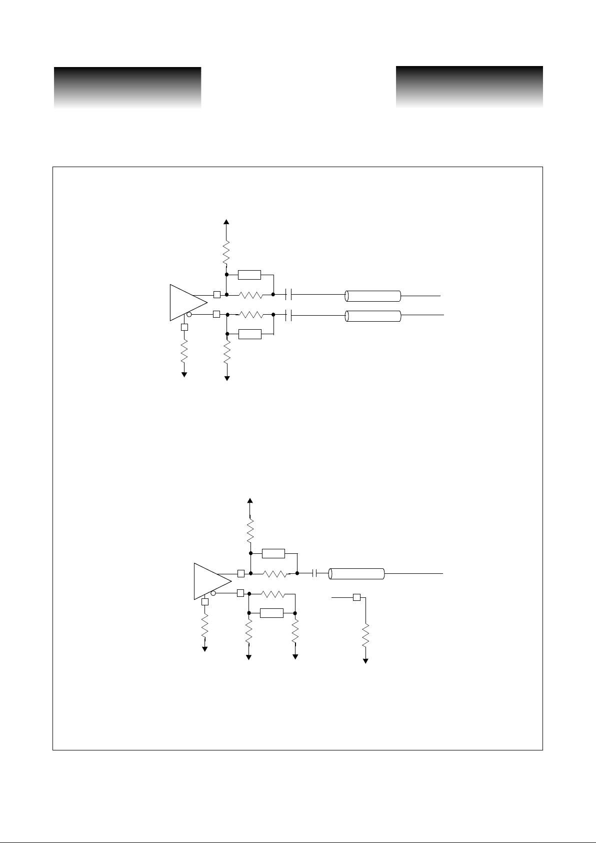
The VSC6501 cable dri v e r output is in te nded to full y compl y with the SMP TE 292M cab le driver specifications. This includes an 800mV swing and a return loss of less than -15dB. The circuit shown below shows how
to connect the output of the VSC6501to the 75 ohm cable and downstream device. The output of the VSC6501
is actually 1200mV. The output termination circuit show n below attenuates the output signal to 800mV and
ensures a return loss better than -15 dB. The ISET resistor is 1.78K
SIGNAL FUNCTION
292M
292M Output:
When HIGH, indicates that the output of the CRU is a SMPTE-292M style signal. This output
combines the analog signal detect with a state machine which monitors SAV/EAV events. If 4000
words occur without an SAV/EAV, then this output goes LOW to indicate invalid data. This output
goes HIGH if the analog signal detection is asserted and an SAV/EAV is located withi n t he l ast 4000
words.
BYPASS
BYPASS Input:
When HIGH, SDI/SDI
are routed around the CRU directly to the SDO0/SDO1 outputs. When LOW,
the output of the CRU is sent to SDO0/SD)1 outputs.
SIGNA L
RECLOCKER
Operation
292M
BYP AS S
Active
Active
O0/O1 Serial Outputs SOURCE IS CRU SDI/SDI
RCLK Output BUFFERED REFCLK
CRU Bypass Mux
SDI/SDI
GOES TO
SDO0/SDO1
SDI/SDI
Serial Input
ACTIVE
SIGDET Output ACTIVE
FRAME Output ACTIVE
1.001 Output ACTIVE
LINE Output ACTIVE
HANC Output ACTIVE
Page 4
VITESSE
SEMICONDUCTOR CORPORATION
Advance Product Information
VSC6501
Cable Driver at 1.485 Gb/s
SMPTE-292M Reclocker and
Page 4
VITESSE
SEMICONDUCTOR CORPORATION
741 Calle Plano, Camarillo, CA 93012 • 805/388-3700 • FAX: 805/987-5896 4/10/00
G52310-0, Rev. 2.0
Draft Copy
Figure 1: High Speed Interconnect Example (Differential)
Figure 2: High Speed Interconnect Example (Single Ended)
6501
V
DD
75
75 ohm Cables
75
75
75
V
DD
1.78K
ISETx
NOTE: All resistors are 1%
10nH
10nH
V
SS
WARNING: SUBJECT TO CHANGE
6501
V
DD
75
75 ohm Coax
75
NOTE: All resistors are 1%
10nH
Optional use of external Voltage Reference provides tighter swing tolerance
1.78K
ISETx
V
SS
75
75
V
DD
10nH
75
V
DD
37.5
V
DD
or
Page 5

VITESSE SEMICONDUCTOR CORPORATION
Page 5
4/10/00 741 Calle Plano, Camarillo, CA 93012 • 805/388-3700 • FAX: 805/987-5896
VITESSE
SEMICONDUCTOR CORPORATION
A
dvance Product Information
VSC6501
and Cable Driver at 1.485 Gb/s
SMPTE-292M Reclocker
G52310-0, Rev. 2.0
Draft Copy
The output swing of the VSC6501 is controlled through the ISETx pins and a VREF input. By connecting
an 1.78K ohm resistor, 1%, between VSS and ISETx the output swing will be controlled to within 800mV +/7%. An optional bandpass v ol tage refere nce may be used to furth er tigh ten t he output swings b y ac curat ely driving the VREF input.
Figure 3: REFCLK Timing Waveforms
Table 3: Reference Clock Requirements *
Note: The PLL locks to the rising edge of REFCLK.
Figure 4: RCLK Timing Waveforms*
Parameters Description Min Max Units Conditions
FR Frequency Range 73.75 74.50 MHz Will accept both 74.176/74.25MHz
FO Frequency Offset -1000 1000 ppm.
Difference in REFCLK frequencies
between the transmitting and receiving
VSC6501s.
DC REFCLK duty cycle -15 +15 % Measured at 1.5V
T
H
, T
L
REFCLK high/low times 3.0 —ns.
Measured between V
IL(MAX)
to V
IL(MAX)
or V
IH(MIN)
to V
IH(MIN)
T
R
REFCLK rise — 2.0 ns. Between V
IL(MAX)
and V
IH(MIN)
REFCLK
V
IL(MAX)
V
IH(MIN)
T
L
T
H
T
R
RCLK
V
IL(MAX)
V
IH(MIN)
T
L
T
H
T
R
Page 6

VITESSE
SEMICONDUCTOR CORPORATION
Advance Product Information
VSC6501
Cable Driver at 1.485 Gb/s
SMPTE-292M Reclocker and
Page 6
VITESSE
SEMICONDUCTOR CORPORATION
741 Calle Plano, Camarillo, CA 93012 • 805/388-3700 • FAX: 805/987-5896 4/10/00
G52310-0, Rev. 2.0
Draft Copy
Absolute Maximum Ratings
(1)
Power Supply Voltage (VDD) .............................................................................................................-0.5V to +4V
PECL DC Input Voltage.........................................................................................................-0.5V to V
DD
+0.5V
TTL DC Input Voltage.......................................................................................................................-0.5V to 5.5V
DC Voltage Applied to TTL Outputs ...................................................................................-0.5V to V
DD
+ 0.5V
TTL Output Current ..................................................................................................................................+/-50mA
PECL Output Current................................................................................................................................+/-50mA
Case Temperature Under Bias.........................................................................................................-55° to +125
o
C
Storage Temperature.......................................................................................................................-65° to + 150
o
C
Maximum Input ESD (Human Body Model).............................................................................................. 1500 V
Recommended Operating Conditions
Power Supply Voltage.................................................................................................... ............. ........3.3V +/- 5%
Ambient Operating Temperature Range...............................................................0°C Ambient to +95°C Case
Notes:
1) CAUTIO N: S tresses listed under “Absolute M ax im u m Rat i ng s ” may be applied t o d evices one at a t i me without causing per-
manent damage. Functional ity at or abo ve the values liste d is not implied. Ex posur e to thes e values for e xtende d periods may
affect device reliability.
DC Characteristics
(Over recommended operating conditions).
Parameters Description Min Typ Max Units Conditions
V
IH
Input HIGH voltage (TTL) 2.0 —5.5 V—
V
IL
Input LOW voltage (TTL) 0 — 0.8 V —
I
IH
Input HIGH current (TTL) — — 500 µA
V
IN
= 2.4 V, 6.8Kohm Pull-up
resistor on all inputs.
I
IL
Input LOW current (TTL) — — -500 µA
VIN = 0.5 V, 6.8Kohm Pull-up
resistor on all inputs.
V
OH
Output HIGH Voltage (TTL) 2.4 — — V I
OH
= -1.0mA
V
OL
Output LOW Voltage (TTL) — — 0.5 V IOL= +1.0mA
V
DD
Supply voltage 3.14 — 3.47 V VDD = 3.3V + 5%
P
D
Power Dissipation: (Estimated) — 800 — mW
Outputs open, V
DD
= VDD
max
(These are estimates)
∆
V
IN
PECL input swing: 200 — 1200 mVp-p
AC Coupled.
Internally biased at V
DD
/2
∆V
OUT75
PECL output swing: 750 — 850 mVp-p
Using appropriate termination
network
Page 7

VITESSE SEMICONDUCTOR CORPORATION
Page 7
4/10/00 741 Calle Plano, Camarillo, CA 93012 • 805/388-3700 • FAX: 805/987-5896
VITESSE
SEMICONDUCTOR CORPORATION
A
dvance Product Information
VSC6501
and Cable Driver at 1.485 Gb/s
SMPTE-292M Reclocker
G52310-0, Rev. 2.0
Draft Copy
Package Pin Descriptions
Figure 5: Pin Diagram
NC
HANC
VDDD
REFCLK
NC
RCLK
VSST
NC
VDDT
NC
NC
NC
VDD
ISET0
VDDD
VSS
VDDD
VREF
ISET1
TEST1
SDO0
D1NC7
VDDT
NC
NC
DNC18
NC
VSST
BYPASS
VDDT
NC
1.001
NC
V53
VSST
SIGDET
CAP1
SCREN
VDDA
NC
CAP0
VSST
VSSA
SDI
VDDD
VDDD
SDI
FRAME
LINE
NC
VDDT
NC
NC
OE0
NC
SDO1
OE1
NC
292M
VSSP
SDO1
VSSP
SDO0
1
3
5
7
9
11
13
15
17 19 21 23 25 27 29 31
63 61 59 57 55 53 51 49
33
35
37
39
41
43
45
47
(Top View)
TEST2
VSC6501
Page 8

VITESSE
SEMICONDUCTOR CORPORATION
Advance Product Information
VSC6501
Cable Driver at 1.485 Gb/s
SMPTE-292M Reclocker and
Page 8
VITESSE
SEMICONDUCTOR CORPORATION
741 Calle Plano, Camarillo, CA 93012 • 805/388-3700 • FAX: 805/987-5896 4/10/00
G52310-0, Rev. 2.0
Draft Copy
Table 3: Pin Identification
Pin # Name Description
2
4
292M
BYPASS
Status Output
Control Input to BYPASS CRU.
50
64
VSS
VDD
Connect with 10k resistor to appropria te signa l.
24 SCREN INPUT - TTL: When HIGH, enables scrambling in Serializer/Deserializer modes
3,7,8,9,11
12,13,47,46
45,43,42,41
40,38,37,36,30
NC No Connect: Leave these pins floating
26 FRAME
OUTPUT - TTL: In Deserializer and Deserializer/Recloc ker mo des, this is a n output wh ich,
when HIGH, indicates that a FRAME synchronization event is on D[0:19].
34 LINE
OUTPUT - TTL: In Deserializer and Deserializer/Recloc ker mo des, this is a n output wh ich,
when HIGH, indicates that a LINE synchronization event is on D[0:19].
27 HANC
OUTPUT- TTL: Output which is HIGH during the Horizontal Blanking period between
EAV and SAV.
25 1.001
OUTPUT - TTL: When HIGH, indicates that a valid receive signal is present on IP/IN and
that the SMPTE-292M incoming data is greater than 500ppm from 20xREFCLK.
21,22 SDI, SDI
INPUT - Differential. Serial input to CRU.
56,54
60,58
SDO0, SDO0
SDO1, SDO1
OUTPUT - Differential. High Speed Cable Driver output.
Serial output from the Reclocker or SDI, SDI
input buffer.
52,62 ISET0, ISET1 Connect resistor to ground to set the output swing of SDO0, SDO1
53,61 OE0, OE1 INPUT - TTL. Out put enable pi ns for SD O0 and SDO1. Ena bled when high for each ou tput.
29 REFCLK
INPUT - TTL. REFerence CLocK at 74.25 MHz. This is the input to the CMU and times
D[19:0] in Serializer Mode.
31 RCLK
OUTPUT - TTL: Output clock. In S eri ali zer a nd Re c lock e r Mo d e, thi s i s a buffered version
of REFCLK. In Deserializer Mode, this is the recovered clock used to time D[19:0]
33 SIGDET
OUTPUT - TTL. An analog signal detect output which, when HIGH, indicates that the SDI
input contains a valid SMPTE-292M amplitude signal.
16,17 CAP0, CAP1 Analog I/O: Loop Filter Capacitor, 0.1uF nominal, 3V swing maxim um
49,19 TEST1, TEST2 INPUT - TTL. LOW for factory test, HIGH for normal operation.
1V53
INPUT - POWER: This power supply would normally be 3.3V. If 5V tolerance is required,
this pin should be connected to 5V supply.
20,23,28,57,51 VDDD Power Supply. 3.3V Supply for digital logic.
5,10,39,44 VDDT TTL I/O Power Supply.
63 VREF Voltage Reference Input. If used, this is biased to 1.25V.
18 VDDA Analog Power Supply. 3.3V for Clock Multiplier PLL. Bypass to pin 15.
55,59 VSSP Ground for High Speed Outputs
14,32,35,48 VSST TTL I/O Ground
15 VSSA Analog Gro und Bypass to pin 18.
Page 9

VITESSE SEMICONDUCTOR CORPORATION
Page 9
4/10/00 741 Calle Plano, Camarillo, CA 93012 • 805/388-3700 • FAX: 805/987-5896
VITESSE
SEMICONDUCTOR CORPORATION
A
dvance Product Information
VSC6501
and Cable Driver at 1.485 Gb/s
SMPTE-292M Reclocker
G52310-0, Rev. 2.0
Draft Copy
Package Thermal Characteristics
The VSC6501 is packaged in an exposed pad, thin quad flat pack (TQFP) which adheres to industry standard EIAJ footprints for a 10x10x1.0mm body, 64 lead TQFP. The package construction is shown below. The
bottom of the lead frame is exposed so that it can be soldered to the printed circuit board and connected to the
ground plane. This provides excellent thermal characteristics and reduces electrical parasitics as well.
Figure 6: Package Cross Section
Table 4: 64-pin, Exposed Pad TQFP Thermal Resistance
The VSC6501 is designed to operate with a case temperature up to 95oC. The user must guarantee that the
case temperature specification is not violated. With the thermal resistances shown above, the VS6501 can operate in still air ambient temperatures of 7 0
o
C [~70oC = 95oC - 0.8W * 30]. If the ambient air temperat ure e xceeds
these limits then some form of coolin g thr ough a hea tsink or an increa se in ai rflo w mu st be pr o vided. Add itional
heat can be transferred to the printed circuit board by not using thermal reliefs on the power and ground plane
vias as well as using multiple vias to the power and ground planes.
If the exposed pad is not sol de re d to t he pr int ed circuit board and grounde d, both thermal and electri cal per -
formance will be degraded significantly.
Moisture Sensitivity Level
This device is rated with a Moisture Sensitivity Level 3 rating. Refer to Application Note AN-2 0 for
appropriate handling procedures.
Symbol Description Value Units
θ
ca-0
Thermal resistance from case to ambient, still air 30
o
C/W
θ
ca-100
Thermal resistance from case to ambien t, 100 LFPM air 25
o
C/W
θ
ca-200
Thermal resistance from case to ambien t, 200 LFPM air 23
o
C/W
θ
ca-400
Thermal resistance from case to ambien t, 400 LFPM air 21
o
C/W
θ
ca-600
Thermal resistance from case to ambien t, 600 LFPM air 20
o
C/W
Die
Plastic Molding Compound
Wire Bond
Ground Bond
Die Attach Epoxy
Copper Lead Frame
Exposed Pad
Page 10

VITESSE
SEMICONDUCTOR CORPORATION
Advance Product Information
VSC6501
Cable Driver at 1.485 Gb/s
SMPTE-292M Reclocker and
Page 10
VITESSE
SEMICONDUCTOR CORPORATION
741 Calle Plano, Camarillo, CA 93012 • 805/388-3700 • FAX: 805/987-5896 4/10/00
G52310-0, Rev. 2.0
Draft Copy
Pac kage Information: 64-pin Exposed Pad TQFP
64 49
1
48
33
3217
G
F
IH
16
11/13o
11/13
0
A
K
A2
0.xxx MAX. LEAD
NONPLANARITY
0.09/0.20
J
0o-7o
E
0.08/0.20 R
0.08 R. MIN.
Item mm Tolerance
A1.20 MAX
A1 0.10 ±0.05
A2 1.00 ±0.05
E0.22 ±0.05
F 12.00 ±0.40
G 10.00 ±0.10
H 12.00 ±0.40
I 10.00 ±0.10
J0.60 ±0.15
K0.50 BSC
Mx.xx ±0.xx
Nx.xx ±0.xx
NOTES:
Drawing not to scale.
A1
M
N
Exposed Pad
(Bottom Side)
Exposed Pad Electrically Grounded
All dimensions in millimeters
Page 11

VITESSE SEMICONDUCTOR CORPORATION
Page 11
4/10/00 741 Calle Plano, Camarillo, CA 93012 • 805/388-3700 • FAX: 805/987-5896
VITESSE
SEMICONDUCTOR CORPORATION
A
dvance Product Information
VSC6501
and Cable Driver at 1.485 Gb/s
SMPTE-292M Reclocker
G52310-0, Rev. 2.0
Draft Copy
Ordering Information
The order number for this product is formed by a combination of the device number, and package type.
Marking Information
The package is marked with three lines of text as shown below.
Figure 7: Package Marking Information
Notice
This document contains informat ion ab out a prod uct duri ng its fabr icati on or ear ly sampli ng phase of development. The information contained in this document is based on design targets, simulation results or early prototype test results. Characteristic data and other specifications are su bject to change without notice. Therefore
the reader is cautioned to confirm that this data sheet is current prior to design or order placement.
Warning
Vi tesse Semico ndu ctor Co rporat ion’s products are not intended for use in l ife supp ort appliances, de v ices or
systems. Use of a Vitesse product in such applications without written consent is prohibited.
VSC6501
RC
Device Type
VSC6501 - HDTV Reclocker
Package Type
RC: 64-Pin, 10x10x1.0mm, Exposed Pad TQFP
Part Number
Pin 1 Identifier
VITESSE
VSC6501 RC
####AAAA
Date Code
Package Suffix
Lot Tracking Code
Page 12

VITESSE
SEMICONDUCTOR CORPORATION
Advance Product Information
VSC6501
Cable Driver at 1.485 Gb/s
SMPTE-292M Reclocker and
Page 12
VITESSE
SEMICONDUCTOR CORPORATION
741 Calle Plano, Camarillo, CA 93012 • 805/388-3700 • FAX: 805/987-5896 4/10/00
G52310-0, Rev. 2.0
Draft Copy
Revision History
2.0 - New Document
 Loading...