

Page 1
VITESSE
SEMICONDUCTOR CORPORATION
Advance Product Information
VSC6108/10/12
Low Jitte
r
Clock Multiplier and Distributo
r
G52224-0, Rev 2.1
VITESSE SEMICONDUCTOR CORPORATION
Page 1
2/15/99
741 Calle Plano, Camarillo, CA 93012 • 805/388-3700 • FAX: 805/987-5896
Features
General Description
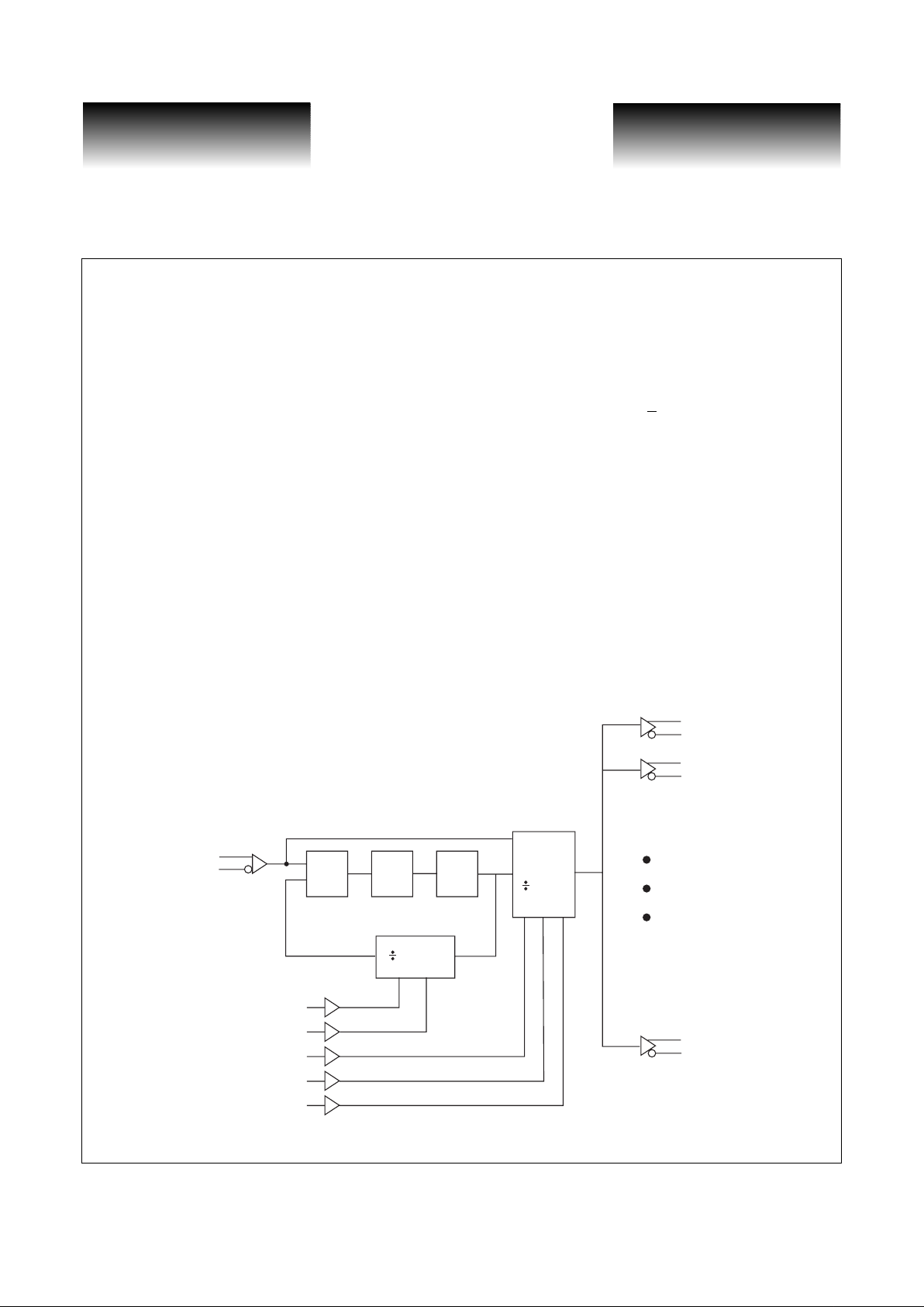
The VSC6108/10/12 are a family of low-jitter clock multiplication and distribution ICs. Each IC uses a
phase locked-loop to lock an on-chip low-noise VCO to an off-chip reference frequency. The VCO output can
be divided down and is output to 18 differential ECL outputs. The VSC6108/10/12 are packaged in a 10 mm x
10 mm 64-pin plastic quad flat pack and consume less than 2 Watts from a single 3.3V power supply.
The VSC6108/10/12 provide high-precision clocks for ATE, instrumentation, telecommunications, datacommunications, and computer system applications where jitter and skew are critical timing parameters. Skew
between outputs is less than 50 ps. Jitter is less than 4 ps rms or 25 ps peak-to-peak. Lock time is 10 µs.
VSC6108/10/12 Functional Block Diagram
• Recommended Companion for VSC6250 500MHz
Deskew IC and Vitesse Timing Generator ICs
• Input Clock Frequency: 50MHz to 622MHz
• Output Clock Frequency: 100MHz to 1.25GHz
• 1 Differential ECL or PECL Clock Input
• 18 Differential ECL or PECL Clock Outputs
• Very Low Jitter: 4ps rms, 25ps Peak-to-Peak
• 10µs Lock Time
• < 50ps Skew Between Outputs
• Single Supply: 3.3V +
5% @ 2 Wa tt s
• Commercial (0
o
to +70oC) Temperature Range
• Package: 10mm x 10mm 64 PQFP
IN
INN
OUT0
OUT0N
OUT1
OUT1N
OUT17
OUT17N
VCO
Loop
Filter
Phase
Detector
Bypass
2,4,8,16
4,8,16,32
FISEL1
FISEL0
FOSEL2
FOSEL1
FOSEL0
Page 2
VITESSE
SEMICONDUCTOR CORPORATION
Advance Product Information
VSC6108/10/12
Low Jitter
C
lock Multiplier and Distributor
Page 2
VITESSE SEMICONDUCTOR CORPORATION
G52224-0, Rev 2.1
741 Calle Plano, Camarillo, CA 93012 • 805/388-3700 • FAX: 805/987-5896
2/15/99
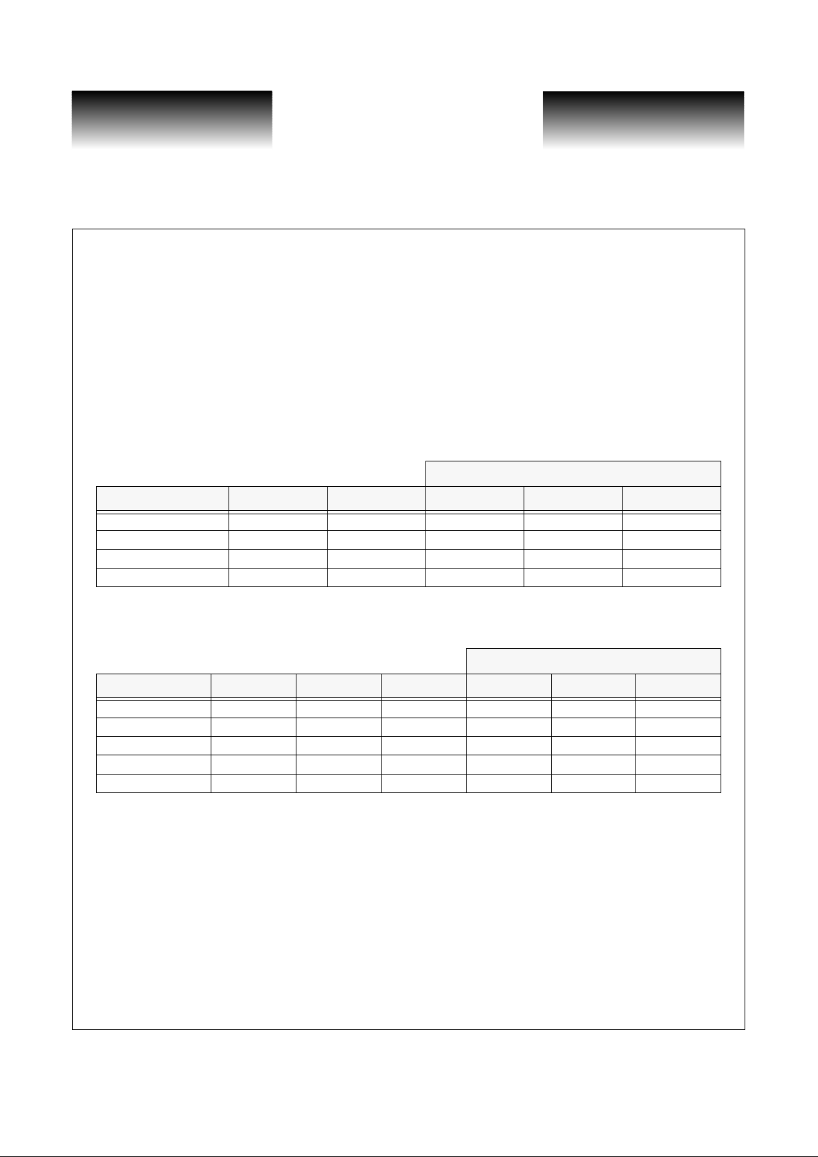
Three versions of the clock multiplier and distributor IC are available.
1. The VSC6108 has a VCO frequency of 1.6 GHz and can output clocks at 800 MHz, 400 MHz, 200 MHz,
and 100 MHz.
2. The VSC6110 has a VCO frequency of 2.0 GHz and can output clocks at 1 GHz, 500 MHz, 250 MHz, and
125 MHz.
3. The VSC6112 h as a VCO frequency of 2. 488 GHz and can o utput clocks at 1.244GHz, 622 MHz, 311MHz,
and 155MHz.
VCO multiplication and ou t put di vi sion ratios a re use r-selectable . Each of the ICs can be co nfig u red for an
input frequency of 1/ 4, 1/8, 1/16, or 1/32 of the VCO fr equency as shown in Table 1 below. The output frequencies are selected as shown in Table 2 below.
Table 1: Input Frequency vs. Mode
Table 2: Output Frequency vs. Mode
f
IN
Mode Name FISEL1 FISEL0 VSC6108 VSC6110 VSC6112
f
VCO
= fIN * 4 0 0 400 MHz 500 MHz 6 22 MHz
f
VCO
= fIN * 8 0 1 200 MHz 250 MHz 311 MHz
f
VCO
= fIN * 16 1 0 100 MHz 125 MHz 155 MHz
f
VCO
= fIN * 32 1 1 50 MHz 62.5 MHz 77.5 MHz
f
OUT
Mode Name FOSEL2 FOSEL1 FOSEL0 VSC6108 VSC6110 VSC6112
f
OUT
= f
IN
000 fIN f
IN
f
IN
f
OUT
= f
VCO
/ 2 0 0 1 800 MHz 1 GHz 1.244GHz
f
OUT
= f
VCO
/ 4 0 1 0 400 MHz 500 MHz 622 MHz
f
OUT
= f
VCO
/ 8 0 1 1 200 MHz 250 MHz 311 MHz
f
OUT
= f
VCO
/ 16 1 0 0 100 MHz 125 MHz 155 MHz
Page 3
VITESSE
SEMICONDUCTOR CORPORATION
Advance Product Information
VSC6108/10/12
Low Jitte
r
Clock Multiplier and Distributo
r
G52224-0, Rev 2.1
VITESSE SEMICONDUCTOR CORPORATION
Page 3
2/15/99
741 Calle Plano, Camarillo, CA 93012 • 805/388-3700 • FAX: 805/987-5896
AC Timing Characteristics
The VSC6108/6110/6112 has an output time jitter of less than 25 ps peak-to-peak. To achieve this jitter
specification the input reference clock must have less than 10 ps peak-to-peak. Output skew is less than 50 ps
between any two outputs.
Table 3: AC Timing Specifications
DC Characteristics
The VSC6108/6110/6112 can be operated from a single 3.3-Volt power supply. Using a -3. 3-Volt supply,
the inputs and outputs are ECL-compatible. Using a +3.3-Volt power supply, the inputs and outputs are PECLcompatible. Total power dissipation is less than 2 Watts.
Table 4: Single Ended ECL Inputs
Note: VEE = -3.3V ± 5%, VCC = GND, Load = 50 to -2.0V , V
REF
= -1.32V ± 25 mV.
Table 5: Differential ECL Inputs and Outputs
Parameter Description Min Typ Max Units
RCd Reference clock duty cycle 40 60 %
RCj Reference clock jitter 10 pSPP
OCd Output clock duty cycle 40 60 %
OCj Output clock OCLK0-17 jitter 25 pSPP
T s k Skew between any ou tp ut clock to any other clock -50 +50 ps
Lr Reference Clock RCK/RCKN frequency range -1.0 +1.0 %
Lt Lock time 10
µS
t
rf
Output rise/fall time 20-80% 100 150 ps
Parameter Description Min Typ Max Units Conditions
V
IH
Input HIGH voltage -1020 - -700 mV
V
IL
Input LOW vol tage -2000 - -1620 mV
Paramet er Description Min Typ Max Units Cond itions
V
IN,DIFF
Input Voltage Differential 200 - - mV
Required input
voltage swing
V
IN,CM
Input Common Mode
Voltage
-1.5 - -0.5 V
Required input
common mode
voltage
V
OUT,DIFF
Output Voltage Differential 400 - 800 mV
Output voltage
swing
V
OUT,CM
Output Common Mode
Voltage
-1.6 - -1.2 V
Common mode
output voltage
Page 4

VITESSE
SEMICONDUCTOR CORPORATION
Advance Product Information
VSC6108/10/12
Low Jitter
C
lock Multiplier and Distributor
Page 4
VITESSE SEMICONDUCTOR CORPORATION
G52224-0, Rev 2.1
741 Calle Plano, Camarillo, CA 93012 • 805/388-3700 • FAX: 805/987-5896
2/15/99
Table 6: Power Dissipation
Note: Output power dissipation does not include load power.
Absolute Maximum Ratings
(1)
Power Supply Voltage, (
V
CC
) ..........................................................................................................-0.5V to +4.3V
Output Current (I
OUT
)....................................................................................................................................50mA
Case Temperature Under Bias (T
C
).............................................................................................-55oC to + 125oC
Storage Temperature (T
STG
) ........................................................................................................-65oC to + 150oC
Note: Caution: Stresses listed under “Absolute Maximum Ratings” may be applied to devices one at a time without causing
permanent damage. Functionality at or exceeding the values listed is not impli ed. Exposure to these values for extended
periods may affect device relia bility.
Recommended Operating Conditions
Power Supply Voltage, (VCC).................................................................................................................+3.3V+5%
Commercial Operating Temperature Range
(2)
(T).............................................................................. 0oC to 70oC
1) CAUTION: Stresses listed under “Absolute Maximum Ratings” may be applied to devices one at a time without causing per-
manent damage. Functiona lity at or above the va lues listed is not impl ied. Expo sure to these values for extended periods may
affect device reliability.
2) Lower limit of specification is ambient temperature and upper limit is case temperature.
ESD Ratings
Proper ESD procedures should be used when handling this product. The VSC6108, VSC6110 and
VSC6112 are rated to the following ESD voltages based on the human body model:
1. All pins are rated at or above 1500V.
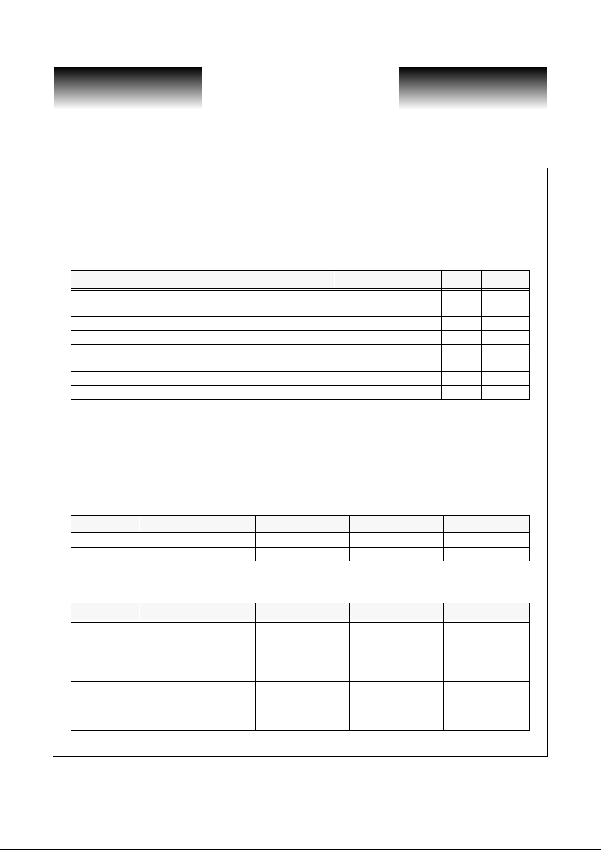
Package Pin Description
Table 7: Package Pin Identification
Description Min Typ Max Units
I
CC
Power supply current 0.45 0.6 A
P
D
Power dissipation 1.5 2 Watts
Pin # Signal Signal Type I/O Type Comments Pin Description
1 VREF Power --- -1.32V Power
2 FOSEL0 I ECL Output Frequency Select 0
3 VEE Power -3.3V Negative Supply Voltage
4 VEE Power -3.3V Negative Supply Voltage
5 FOSEL1 I ECL Output Frequency Select 1
6 FOSEL2 I ECL Output Frequency Select 2
Page 5

VITESSE
SEMICONDUCTOR CORPORATION
Advance Product Information
VSC6108/10/12
Low Jitte
r
Clock Multiplier and Distributo
r
G52224-0, Rev 2.1
VITESSE SEMICONDUCTOR CORPORATION
Page 5
2/15/99
741 Calle Plano, Camarillo, CA 93012 • 805/388-3700 • FAX: 805/987-5896
7 VCC Power 0V Positive Sup p ly Voltage
8 FISEL1 I ECL Input Frequency Select 1
9 FISEL0 I ECL Input Frequency Select 0
10 VEE Power -3.3V Negative Supply Voltage
11 not used --- --- n/c
12 not used --- --- n/c
13 VCC Power 0V Positive Supply Voltage
14 VEE Power -3.3V Negative Supply Voltage
15 IN I ECL Input Clock
16 INN I ECL Input Clock Inverted
17 OUT0 O ECL O utput 0
18 OUT0N O ECL Output 0 Inverted
19 VEE Power -3.3V Negative Supply Voltage
20 OUT1 O ECL O utput 1
21 OUT1N O ECL Output 1 Inverted
22 OUT2 O ECL O utput 2
23 OUT2N O ECL Output 2 Inverted
24 OUT3 O ECL O utput 3
25 OUT3N O ECL Output 3 Inverted
26 VCC Power 0V Positive Supply Voltage
27 OUT4 O ECL O utput 4
28 OUT4N O ECL Output 4 Inverted
29 OUT5 O ECL O utput 5
30 OUT5N O ECL Output 5 Inverted
31 VEE Power -3.3V Negative Supply Voltage
32 VCC Power 0V Positive Supply Voltage
33 OUT6 O ECL O utput 6
34 OUT6N O ECL Output 6 Inverted
35 OUT7 O ECL O utput 7
36 OUT7N O ECL Output 7 Inverted
37 VCC Power 0V Positive Supply Voltage
38 OUT8 O ECL O utput 8
39 OUT8N O ECL Output 8 Inverted
Pin # Signal Signal Type I/O Type Comments Pin Description
Page 6

VITESSE
SEMICONDUCTOR CORPORATION
Advance Product Information
VSC6108/10/12
Low Jitter
C
lock Multiplier and Distributor
Page 6
VITESSE SEMICONDUCTOR CORPORATION
G52224-0, Rev 2.1
741 Calle Plano, Camarillo, CA 93012 • 805/388-3700 • FAX: 805/987-5896
2/15/99
Note:(1) The pin description above assumes that VEE is connected to -3.3 Volts, VCC is connected to 0 Volts, VREF is connected
to -1.32 Volts, and all I/Os are ECL. If the device is operated using a +3.3 Volt power supply, VCC should be connected
to +3.3 Volts and VEE should be connected to 0 Volts. In this case, I/Os are PECL and VREF should be connected to
+1.98 Volts.
40 OUT9 O ECL O utput 9
41 OUT9N O ECL Output 9 Inverted
42 VCC Power 0V Positive Supply Voltage
43 OUT10 O ECL Output 10
44 OUT10N O ECL O utput 10 Inverted
45 VEE Power -3.3V Negative Supply Voltage
46 OUT11 O ECL Output 11
47 OUT11N O ECL Output 11 Inverted
48 VCC Power 0V Positive Supply Voltage
49 VEE Power -3.3V Negative Supply Voltage
50 OUT12N O ECL O utput 12 Inverted
51 OUT12 O ECL Output 12
52 OUT13N O ECL O utput 13 Inverted
53 OUT13 O ECL Output 13
54 VCC Power 0V Positive Supply Voltage
55 OUT14N O ECL O utput 14 Inverted
56 OUT14 O ECL Output 14
57 OUT15N O ECL O utput 15 Inverted
58 OUT15 O ECL Output 15
59 VCC Power 0V Positive Supply Voltage
60 OUT16N O ECL O utput 16 Inverted
61 OUT16 O ECL Output 16
62 VEE Power -3.3V Negative Supply Voltage
63 OUT17N O ECL O utput 17 Inverted
64 OUT17 O ECL Output 17
Pin # Signal Signal Type I/O Type Comments Pin Description
Page 7

VITESSE
SEMICONDUCTOR CORPORATION
Advance Product Information
VSC6108/10/12
Low Jitte
r
Clock Multiplier and Distributo
r
G52224-0, Rev 2.1
VITESSE SEMICONDUCTOR CORPORATION
Page 7
2/15/99
741 Calle Plano, Camarillo, CA 93012 • 805/388-3700 • FAX: 805/987-5896
Package Information
64 49
1
48
33
3217
G
F
IH
L
16
10o TYP
100 TYP
A
K
D
0.102 MAX. LEAD
COPLANARITY
0.17 MAX.
A
0.25
J
0o- 8o
0.25 MAX.
E
0.30 RAD. TYP.
0.20 RAD. TYP.
STANDOFF
Item mm Tol.
A2.45 MAX
D 2.00 +0.10
E0.30 ±.05
F 13.20 ±.25
G 10.00 ±.10
H 13.20 ±.25
I 10.00 ±.10
J 0.88 ±.15
K0.50BASIC
L 3.56 ±.50 DIA.
NOTES:
Drawing not to scale.
Heat spreader up.
All units in mm unless otherwise noted.
Heat spreader is not electrically connected.
64-Pin Thermally Enhanced PQFP
Page 8

VITESSE
SEMICONDUCTOR CORPORATION
Advance Product Information
VSC6108/10/12
Low Jitter
C
lock Multiplier and Distributor
Page 8
VITESSE SEMICONDUCTOR CORPORATION
G52224-0, Rev 2.1
741 Calle Plano, Camarillo, CA 93012 • 805/388-3700 • FAX: 805/987-5896
2/15/99
Package Thermal Characteristics
The VSC6108/10/12 is packaged into a thermally-enhanced plastic quad flatpack (PQFP). This package
adheres to the industry-st andard E I AJ footp r in t f or a 10x 10mm body but has been enhanced to improve thermal
dissipation with the inclusion of an exposed Copper Heat Spreader. The package construction is as shown in
Figure 1.
Figure 1: Package Cross Section
The thermal resistance is improved through low the rmal resistance paths from the die to the exposed su rface of the heat spreader and from the die to the lead frame through t he h eat spreader overlap of the lead frame.
Table 8: 64-Pin PQFP Thermal Resistance
The VSC6108/10/12 is designed to operate at a maximum case temperature of up to 70 oC. The user must
guarantee that the maximum case temperature specification is not violated, most applications will require a
heatsink.
Symbol Description Value Units
θ
jc
Thermal resistance fr om junction to case 2.5
o
C/W
θ
ca
Thermal resistance from case to ambient in still air including conduction through
the leads for a non-thermally saturate d board.
37
o
C/W
θ
ca-100
Thermal resistance from case to ambien t in 100 LPFM air 31
o
C/W
θ
ca-200
Thermal resistance from case to ambien t in 200 LPFM air 28
o
C/W
θ
ca-400
Thermal resistance from case to ambien t in 400 LPFM air 24
o
C/W
θ
ca-600
Thermal resistance from case to ambien t in 600 LPFM air 22
o
C/W
Lead
Copper Heat Spreader
Die
Plastic Molding Compound
Insulator
Wire Bond
Page 9

VITESSE
SEMICONDUCTOR CORPORATION
Advance Product Information
VSC6108/10/12
Low Jitte
r
Clock Multiplier and Distributo
r
G52224-0, Rev 2.1
VITESSE SEMICONDUCTOR CORPORATION
Page 9
2/15/99
741 Calle Plano, Camarillo, CA 93012 • 805/388-3700 • FAX: 805/987-5896
Notice
This document contains in formation abou t a product durin g its fabrication or ea rly sampling phas e of
development. The information contained in this document is based on design targets, simulation results or early
prototype test results. Characteristic data and other specifications are subject to change without notice. Therefore the reader is cautioned to confirm that this datasheet is current prior to design or order placement.
Warning
Vitesse Semiconductor Corporation’s product are not intended for use in life support appliances, devices or
systems. Use of a Vitesse product in such applications without written consen t is prohibited.
Page 10

VITESSE
SEMICONDUCTOR CORPORATION
Advance Product Information
VSC6108/10/12
Low Jitter
C
lock Multiplier and Distributor
Page 10
VITESSE SEMICONDUCTOR CORPORATION
G52224-0, Rev 2.1
741 Calle Plano, Camarillo, CA 93012 • 805/388-3700 • FAX: 805/987-5896
2/15/99
 Loading...