

Page 1
VITESSE SEMICONDUCTOR CORPORATION
Page 1
8/28/00 741 Calle Plano, Camarillo, CA 93012 • 805/388-3700 • FAX: 805/987-5896
VITESSE
SEMICONDUCTOR CORPORATION
Data Sheet
SC6048
G52335-0, Rev. 4.0
High-Speed Octal
Programmable Timing Generator
Features
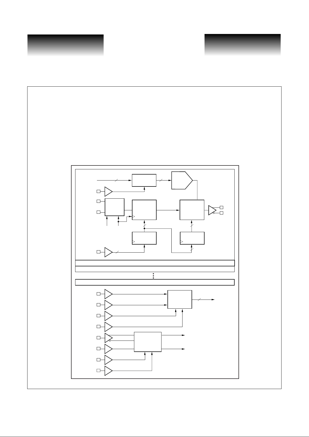
VSC6048 Block Diagram
• 100MHz/200MHz Dynamic Reprogram Frequency
for Incrementing and Decrementing
• Internal or External High-Speed Clock Option
• Low Power: 8 Watts, max
• Low Cost 160-Pin PQFP Packaging
• 8 Fully Integrated Timing Generators for ATE
Applications
• 10/5ns Delay Range, 10ps Resolution
• Fully Digital Interface. No Off-Chip DACs or
Trim Components Required
• ± 4 LSB Differential Non-Linearity
DAC_WR
CAL_DAT
Register
SPAN
CAL
DAC
IN0A
IN0B
DIN
TEST[0:9]
Register
Channel 1
Channel 0
Channel 2
Channel 7
Variable
Shift
Register
Input
Interleve
800MHz
Clock
400MHz
Clock
3
Vernier
Delay
Element
Out 0
Calibration
Register
400MHz Clock
800MHz Clock
PLL
Clock Multiplier
Unit
x8, x16
Register
7
7
10
6
CAL_DAT
6
6
ADR[0:2]
DCLK
SHIFT
RCK
RCKN
BYP
FSEL
PLLRST
Page 2
VITESSE
SEMICONDUCTOR CORPORATION
Data Sheet
VSC6048
High-Speed Oct al
Programmable Timing Generator
Page 2
VITESSE SEMICONDUCTOR CORPORATION
741 Calle Plano, Camarillo, CA 93012 • 805/388-3700 • FAX: 805/987-5896 8/28/00
G52335-0,Rev.4.0
Functional Description
Reference Clock Selection
Clock multiplication of x8 or x16 may be selected via the FSEL pin, requiring a reference clock of 100
±2.5MHz or 50 ±1.25MHz, respectively. For system applications with 800MHz on board clock, the CMU can
be bypassed by asserting BYP signal and RCK will accept an external 800MHz clock.
In Bypass mode (BYP = 1, RCK = 800MHz) the skew from INX to RCK at the pin is 550ps +/-250ps.
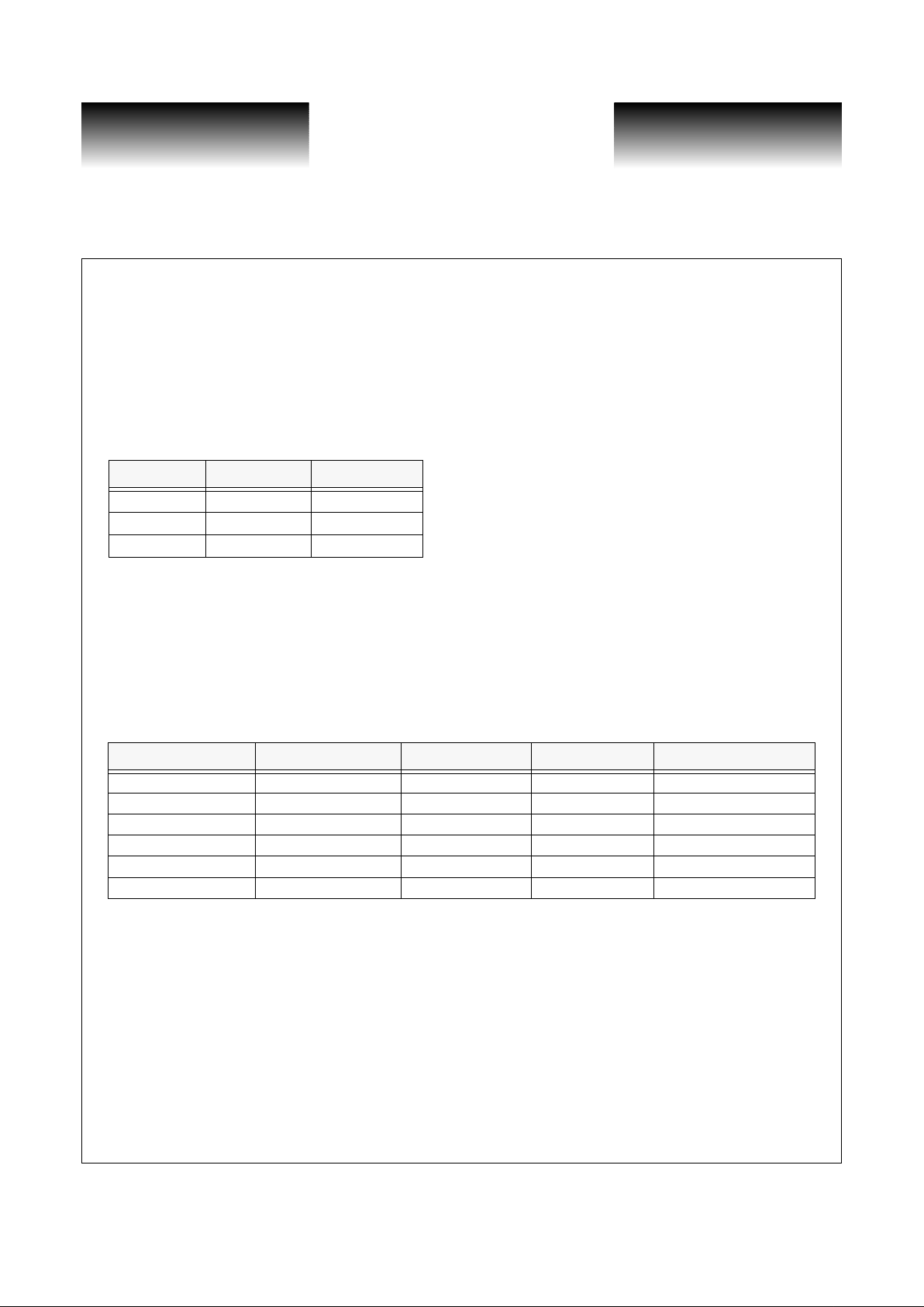
Ta ble 1: Reference Clock Selection
X = don’t care.
Mode of Operations
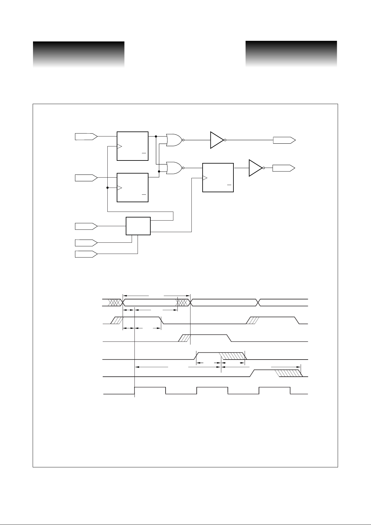
There are 6 basic modes of operatio n. These mod es are based on t wo input s per channel (INA a nd INB) t hat
can be interleaved and refire rate. The maximum refire rate for full 10ns span is 100MHz, where the maximum
refire rate for 5ns span is 200MHz. The maximum refire rate at the input to the fine vernier must not be sooner
than 4 cycles of the high-speed clock (800MHz).
T able 2: Suggested Operating Modes
Data Input (INA, INB)
There are two interleaved inputs per channel. Each input is capable of running at full rate (200MHz). The
input is first retimed off of the inte rnal 400MHz cl ock generate d from the PLL. This means t here is a 2.5ns edge
placement window that defines the setup time. This also means that the input pulse must span at least one
400MHz clock edge.
The inputs are low to high edge sensitive. Figure 1 illustrates an equivalent circuit of the input structure for
each channel. Note that the TSET input clock is generated based on the input data.
BYP FSEL RCK
0
0100MHz
0
150MHz
1
X800MHz
Program Rate Interleaved INA INB TSET[0:9] Range
200Mbps Yes 100MHz 100MHz 000 to 1FF
100Mbps Yes 50MHz 50MHz 000 to 3FF
200Mbps No 200MHz Low 000 to 1F F
100Mbps No 100MHz Low 000 to 3F F
200Mbps No Low 200MHz 000 to 1FF
100Mbps No Low 100MHz 000 to 3FF
Page 3
VITESSE SEMICONDUCTOR CORPORATION
Page 3
8/28/00 741 Calle Plano, Camarillo, CA 93012 • 805/388-3700 • FAX: 805/987-5896
VITESSE
SEMICONDUCTOR CORPORATION
Data Sheet
SC6048
G52335-0, Rev. 4.0
High-Speed Octal
Programmable Timing Generator
Figure 1: Input Interleave
Figure 2: Functional Timing Diagram
Time Set Input (TSET<0:9>)
This is a 10-bit TTL bus that controls the delay value of the vernier. The 3 MSBs cont rol the 800MHz shift
register and the 7 LSBs control the fine delay element. The TSET data is clocked in by a pulse generated from
the input data. The setup time o f the TSET data is the same as the input signals (INA, INB). The TSET data
must be stable by the time the input edge arrives at the input pin and data m ust then be held stable for at leas t
3.5ns after the input edge arrives at the pin.
TSET_CLK
D
SET
CLR
Q
DQ
D
SET
CLR
Q
DQ
D
SET
PLL
CLR
400MHz
800MHz
Q
DQ
DATA
INxA
INxB
RCK
FSEL
BYP
t
RATETS
t
SETH
t
SETSU
IN
SU
t
OPW
t
PDV(SPAN)
t
PDTG(SPAN)
t
PDTG(MIN)
TSET[0:9]
INA
INB
RCK
OUT
TSET (0000000000)
OUT
TSET (1111111111)
IN
H
Page 4

VITESSE
SEMICONDUCTOR CORPORATION
Data Sheet
VSC6048
High-Speed Oct al
Programmable Timing Generator
Page 4
VITESSE SEMICONDUCTOR CORPORATION
741 Calle Plano, Camarillo, CA 93012 • 805/388-3700 • FAX: 805/987-5896 8/28/00
G52335-0,Rev.4.0
Figure 3: Fine Vernier Calibration DAC Programming
DAC Calibration
Each fine vernier must be calibrated to a 1240ps span, one step (10ps) shorter than the 800MHz period
(1.25ns). This is accomplished by setting the fine vernier to maximum delay and adjusting the 6-bit calibration
DAC until the desired range has been achieved.
The calibration data is transferred into the device through a 3-bit serial interface. Refer to Figure 3 for the
programming sequence. Typical DCLK frequencies are 1MHz to 10MHz. Once the calibration value has been
transferred into the device, the data is written into the specified DAC by the r ising edge of DCLK when
DAC_WR is HIGH. The address lines must remain stable from the enable of SHIFT to one cycle after the disable of DAC_WR.
DAC Application
There are three DAC_REF pins on this device. Each pin supplies the reference for two or three calibration
DACs. In order to reduce crosstalk between verniers through the DAC_REF supply, it is recommended that
each DAC_REF pin be isolat ed from each other. This will reduce crosstalk b etween the the three channel
groups, however, it will not effect crosstalk between verniers within each group.
Table 3: DAC Reference Pin Identification
Outputs
Each channel has a differential ECL output. The output of the verniers is falling edge active. The shift reg-
ister propagates a 2ns pulse. The fine vernier then stretches the pulse width based on the programmed delay.
DAC_REF Pin # Vernier Channels
10, 1, 2
18 3, 4
40 5, 6, 7
SHIFT
DCLK
DIN
DAC_WR
CAL_DAT
(internal)
ADR[2:0]
543210
Vernier 0 DAC Data
XXXXX 543210XXXX
1
23456
1
23456
Address for Vernier 0
Vernier 1 DAC Data
Address for Vernier 1
Shift Data Into
Calibration Register
Hold Data In
Calibration Register
One T est/Calibration Cycle
Page 5
VITESSE SEMICONDUCTOR CORPORATION
Page 5
8/28/00 741 Calle Plano, Camarillo, CA 93012 • 805/388-3700 • FAX: 805/987-5896
VITESSE
SEMICONDUCTOR CORPORATION
Data Sheet
SC6048
G52335-0, Rev. 4.0
High-Speed Octal
Programmable Timing Generator
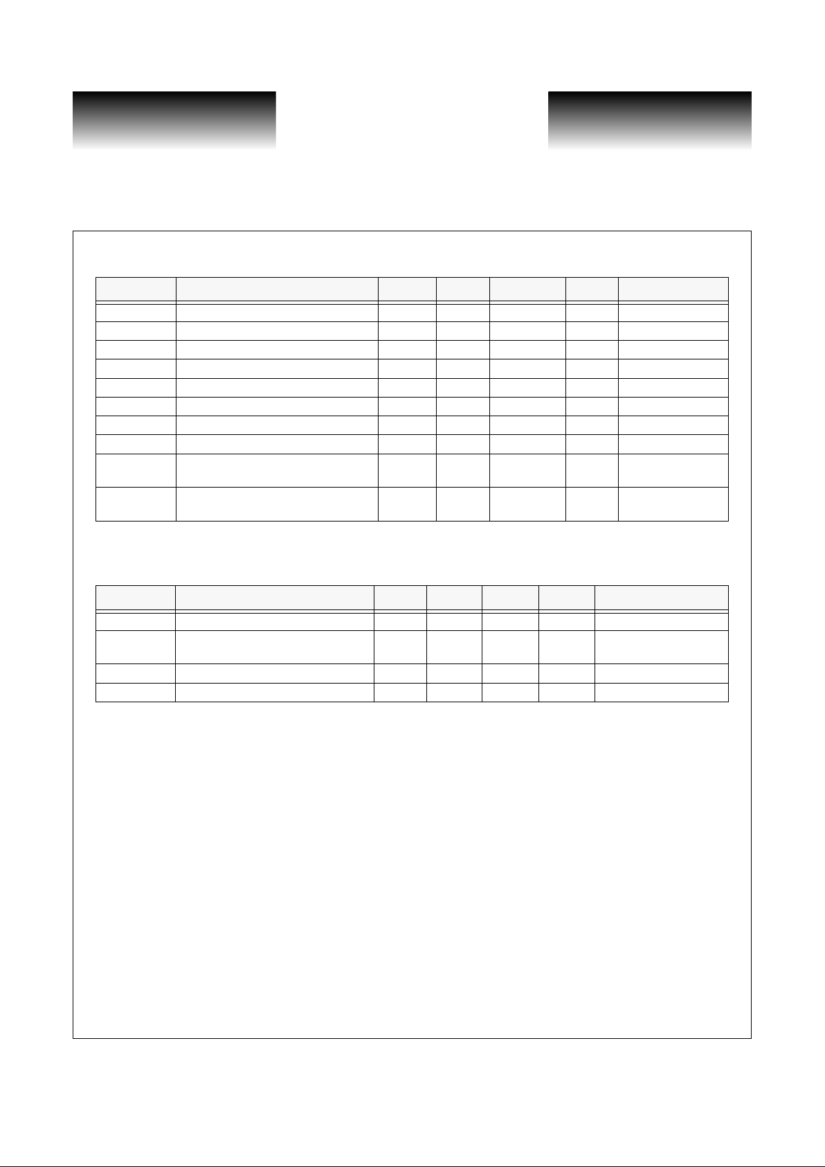
DC Characteristics
Table 4: Single Ended ECL Inputs and Outputs
NOTE: VTT = -2.0V ± 5%, VCC = V
CCA
= GND, R
LOAD
= 50Ω to -2.0V.
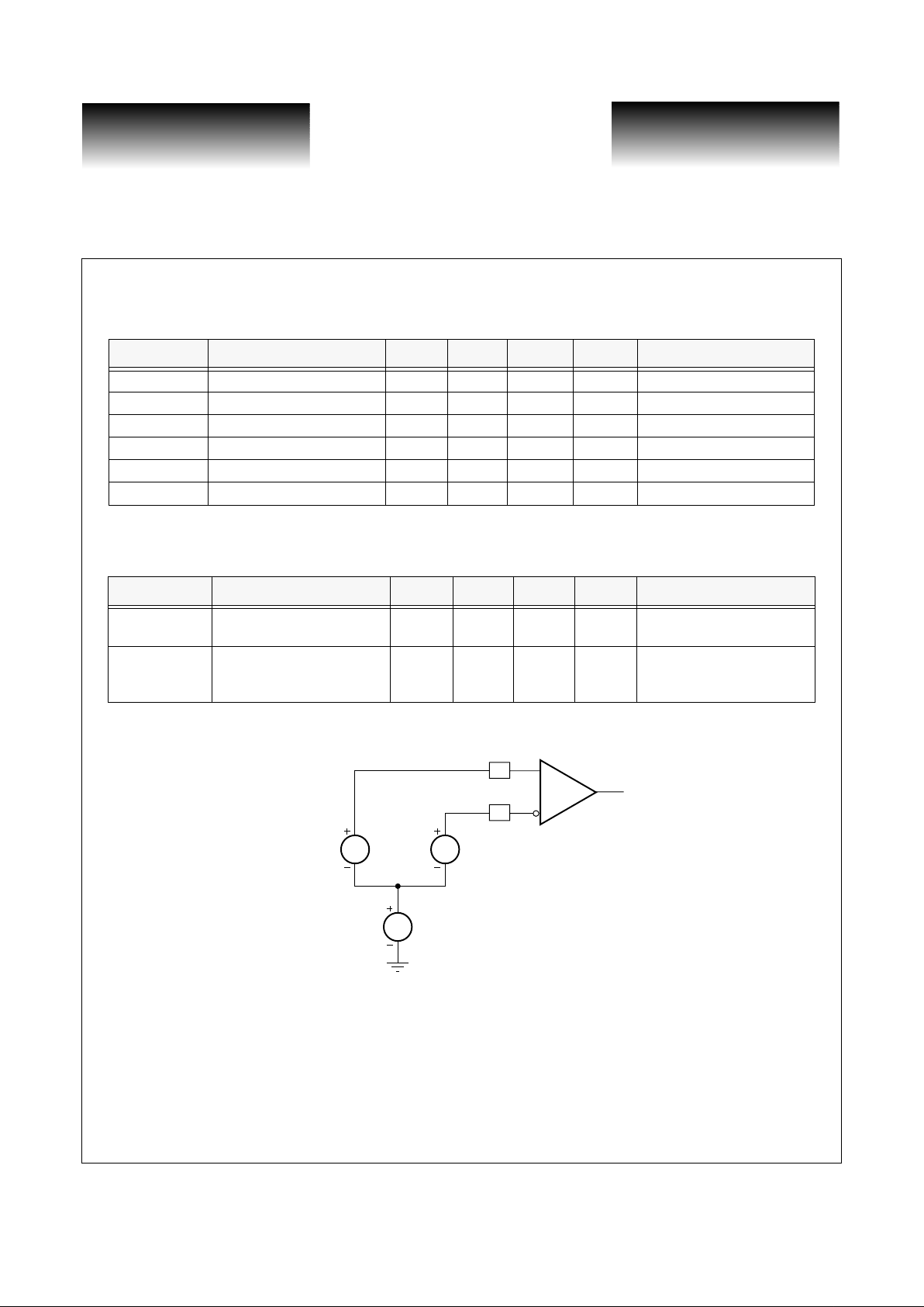
Table 5: Differential ECL Inputs and Outputs
Figure 4: Differential ECL Input Voltages
Parameter Description Min Typ Max Units Conditions
V
OH
Output HIGH Voltage -1020 - -700 mV
V
OL
Output LOW Voltage -2000 - -1620 mV
V
IH
Input HIGH Voltage -1165 - -700 mV
V
IL
Input LOW Voltage -2000 - -1475 mV
I
IH
Input HIGH Current - - 200 uA V
IN
= VIH (max)
I
IL
Input LOW Current -50 - - uA V
IN
= VIL (min)
Parameter Description Min Typ Max Units Conditions
V
DIFF
Input Voltage Differential 200 - - mV
Required for full output
swing
V
CM
Common-Mode Voltage -1.5 - -0.5 V
Common-mode range
required for full output swing
with V
DIFF
applied
V
DIFF
/2
V
CM
V
DIFF
/2
Pad
PadN
Page 6
VITESSE
SEMICONDUCTOR CORPORATION
Data Sheet
VSC6048
High-Speed Oct al
Programmable Timing Generator
Page 6
VITESSE SEMICONDUCTOR CORPORATION
741 Calle Plano, Camarillo, CA 93012 • 805/388-3700 • FAX: 805/987-5896 8/28/00
G52335-0,Rev.4.0
Table 6: TTL Inputs and Outputs
NOTE: All specifications are over recommended commercial operating conditions, TTL/GND = GND.
Table 7: Power Supply Requirements
NOTE: (1) Output power dissipation does not include load power.
Parameter Description Min Typ Max Units Conditions
V
OH
Output HIGH Voltage 2.4 - - V I
OH
= -2.4mA
V
OL
Output LOW Voltage 0 - 0.4 V I
OL
= 16 mA
V
IH
Input HIGH Voltage 2.0 - V
TTL
+1.0V V -
V
IL
Input LOW Voltage 0 - 0.8 V -
I
IH
Input HIGH Current - - 50 µA V
IN
= 2.4V
I
IL
Input LOW Current -500 - - µA V
IN
= 0.4V
I
OZH
Tri-State Ou tp ut O FF Curren t HIGH - - 200 µA V
OUT
= 2.4V
I
OZL
Tri-State Output OFF Curre n t LOW -100 - - µA V
OUT
= 0.4V
I
OZLB
Tri-State Output OFF Current Low for
Bi-directs
-600 - - µA
V
OUT
= 0.4V
I
OCZ
Open Collector Output Leakage
Current
--200µA
V
OUT
= 2.4V
Parameter Description
Min
Typ Max Units Conditions
I
TT
Power Supply Current from V
TT
3.4 mA
I
DACREF
Power Supply Current from
V
DACREF
80 mA
I
TTL
Power Supply Current from V
TTL
250 mA
P
D
Power Dis sipation
(1)
8W
Page 7

VITESSE SEMICONDUCTOR CORPORATION
Page 7
8/28/00 741 Calle Plano, Camarillo, CA 93012 • 805/388-3700 • FAX: 805/987-5896
VITESSE
SEMICONDUCTOR CORPORATION
Data Sheet
SC6048
G52335-0, Rev. 4.0
High-Speed Octal
Programmable Timing Generator
Ta ble 8: AC Characteristics
NOTE: (1) The rising edge of the input (INA, INB) must fall in the setup region defined from 250ps to 1250ps before the rising
edge of the reference clock (RCK, RCKN).
Parameter Description Min Typ Max Units
t
RATE IN
INA and INB Reprogram Rate 5 ns
t
RATE TS
TSET Reprogram Rate, 200MHz Application 5 ns
t
RATE TS
TSET Reprogram Rate, 100MHz Application 10 ns
t
RES
Nominal Resolution (t
PDV(SPAN)
/ 127) 10 ps
t
SPAN
Propagation Delay, 200MHz Application
Full TG Sp an (TSET = 0011111111)
After Vernier Span DAC Calibration
4980 4990 ps
t
PDTG(SPAN)
Propagation Delay, 100MHz Application
Full TG Sp an (TSET = 1111111111)
After Vernier Span DAC Calibration
9980 9990 ps
t
PDV(SPAN)
Propagation Delay
Vernier Delay Element Span (TSET=0001111111)
After Vernier Span DAC Calibration
1230 1240 ps
t
PDTG(MIN)
Propagation Delay
TG Minimum Delay (TSET= 000000000)
11.0 14.0 ns
t
PDV(MIN)
Propagation Delay
Vernier Delay Element Zero Delay
1300 1700 ps
INL
Integral Non-Linearity
Dynamic on-the-fly TSET Switching
-4 +4 LSBs
DNL
Differential Non-Linearity
Dynamic on-the-fly TSET Switching
-4 +4 LSBs
DCV
Variation in Delay vs. Duty Cycle and Frequency
Full TG Span (TSET=1111111111)
-40 +40 ps
D
TCO
Variation in Delay vs. Temperature
Full TG Span (TSET=1111111111)
-6 +6 ps/°C
PSRR
Variation in Delay vs. Supply Voltage
Full TG Span (TSET=1111111111)
-8 +8 ps/100mV
OSJ Random Output Signal Jitter 10 ps rms
DAC
RES
Calibration DAC Resolution 25 ps
t
OPW
Width of the Output Pulse 800 2500 ps
tR/t
F
Output Rise/Fall Times (20% to 80%) 300 ps
IN
SU
IN0 - IN7 to REF_CLK Setup
(1)
250 1250 ps
IN
H
IN0 - IN7 to REF_CLK Hold
(1)
1750 ps
t
SETSU
TSET [0:9] Setup with Respect to IN 250 ps
t
SETH
TSET [0:9] Hold with Respect to IN 3500 ps
IN
PW
IN0 - IN7 Pulse Width 2 ns
Page 8

VITESSE
SEMICONDUCTOR CORPORATION
Data Sheet
VSC6048
High-Speed Oct al
Programmable Timing Generator
Page 8
VITESSE SEMICONDUCTOR CORPORATION
741 Calle Plano, Camarillo, CA 93012 • 805/388-3700 • FAX: 805/987-5896 8/28/00
G52335-0,Rev.4.0
Absolute Maximum Ratings
(1)
Power Supply Voltage (VTT) ..........................................................................................................-2.5V to +0.5V
Power Supply Voltage (V
DACREF
) .................................................................................................-0.5V to +4.3V
Power Supply Voltage (V
TTL
) ........................................................................................................-0.5V to +4.3V
ECL Input Voltage Applied, (V
IN ECL
) ................................................................................+0.5V to VTT + -0.5V
TTL Input Voltage Applied, (V
IN TTL
)................................................................................. -0.5V to V
TTL
+ 1.0V
Output Current (I
OUT
)...................................................................................................................................50mA
Case Temperature Under Bias (T
C
) .............................................................................................-55oC to + 125oC
Storage Temperature (T
STG
)........................................................................................................-65oC to + 150oC
Recommended Operating Conditions
Power Supply Voltage (VTT)..................................................................................................................-2.0V %
Power Supply Voltage (V
DACREF
)........................................................................................................+3.0V %
Power Supply Voltage (V
TTL
)...............................................................................................................+3.3V %
Commercial Operating Temperature Range
(2)
(T).............................................................................. 0oC to 70oC
NOTES: (1) Caution: Str e sse s listed un der “Abso lute Ma xi mum Ratin gs” may be app lied to dev ices on e at a time with out cau sing
permanent damage. Functionality at or above the values listed is not implied. Exposure to these values for extended
periods may affect device reliability.
(2) Lower limit of specification is ambient temperature and upper limit is case temperature.
ESD Ratings
Proper ESD procedures should be used when handling this product. The VSC6048 is rated to the following
ESD voltages based on the human body model:
1. All pins are rated at or above 1500V.
5±
5±
5±
Page 9

VITESSE SEMICONDUCTOR CORPORATION
Page 9
8/28/00 741 Calle Plano, Camarillo, CA 93012 • 805/388-3700 • FAX: 805/987-5896
VITESSE
SEMICONDUCTOR CORPORATION
Data Sheet
SC6048
G52335-0, Rev. 4.0
High-Speed Octal
Programmable Timing Generator
Package Pin Description
Figure 5: Pin Diagram
VITESSE
VSC6048
DAC_REF
VCC
TSET35
TSET36
TSET37
TSET38
TSET39
VTT
IN0A
IN0B
IN1A
IN1B
IN2A
IN2B
IN3A
IN3B
VCC
DAC_REF
VPLL
VGND
RCK
RCKN
VCC
VGND
VPLL
VTT
IN4A
IN4B
IN5A
IN5B
IN6A
IN6B
IN7A
IN7B
VCC
TSET40
TSET41
TSET42
VTT
DAC_REF
TSET00
VCC
BYP
FSEL
ADR2
ADR1
ADR0
OUT0N
OUT0
VCC
OUT1N
OUT1
VTT
OUT2N
OUT2
VCC
OUT3N
OUT3
NC
OUT4N
OUT4
VTT
OUT5N
OUT5
VTT
OUT6N
OUT6
VTT
OUT7N
OUT7
DCLK
SHIFT
VCC
DAC_WR
PLLRST
DIN
VCC
TSET79
TSET78
TSET77
1
2
3
4
5
6
7
8
9
10
11
12
13
14
15
16
17
18
19
20
21
22
23
24
25
26
27
28
29
30
31
32
33
34
35
36
37
38
39
40
120
119
118
117
116
115
114
113
112
111
110
109
108
107
106
105
104
103
102
101
100
99
98
97
96
95
94
93
92
91
90
89
88
87
86
85
84
83
82
81
TSET43
TSET44
TSET45
TSET46
TSET47
TSET48
TSET49
TSET50
VCC
TSET51
TSET52
TSET53
TSET54
TSET55
TSET56
TSET57
VTT
TSET58
TSET59
TSET60
TSET61
TSET62
TSET63
VCC
TSET64
TSET65
TSET66
TSET67
TSET68
TSET69
TSET70
VTTL
TSET71
TSET72
TSET73
TSET74
TSET75
TEST76
VTT
VCC
TSET34
TSET33
TSET32
TSET31
TSET30
VTT
TSET29
TSET28
TSET27
TSET26
TSET25
TSET24
TSET23
VCC
TSET22
TSET21
TSET20
TSET19
TSET18
TSET17
VTT
TSET16
TSET15
TSET14
TSET13
TSET12
TSET11
TSET10
VTTL
TSET09
TSET08
TSET07
TSET06
TSET05
TSET04
TSET03
TSET02
TSET01
VCC
VTT
414243444546474849505152535455565758596061626364656667686970717273747576777879
80
160
159
158
157
156
155
154
153
152
151
150
149
148
147
146
145
144
143
142
141
140
139
138
137
136
135
134
133
132
131
130
129
128
127
126
125
124
123
122
121
Page 10

VITESSE
SEMICONDUCTOR CORPORATION
Data Sheet
VSC6048
High-Speed Oct al
Programmable Timing Generator
Page 10
VITESSE SEMICONDUCTOR CORPORATION
741 Calle Plano, Camarillo, CA 93012 • 805/388-3700 • FAX: 805/987-5896 8/28/00
G52335-0,Rev.4.0
Table 9: Pin Identifications
Pin # Signal Name Signal Type Levels Description
1 DAC_REF — +3.0V DAC Reference Supply
2 VCC — 0V Ground
3 TSET35 TTL I Timeset Data for Channel 3, Bit 5
4 TSET36 TTL I Timeset Data for Channel 3, Bit 6
5 TSET37 TTL I Timeset Data for Channel 3, Bit 7
6 TSET38 TTL I Timeset Data for Channel 3, Bit 8
7 TSET39 TTL I Timeset Data for Channel 3, Bit 9
8 VTT — -2.0V Power Supply
9 IN0 A ECL I Channel 0, Input A
10 IN0B ECL I Channel 0, Input B
11 IN1A ECL I Channel 1, Input A
12 IN1B ECL I Channel 1, Input B
13 IN2A ECL I Channel 2, Input A
14 IN2B ECL I Channel 2, Input B
15 IN3A ECL I Channel 3, Input A
16 IN3B ECL I Channel 3, Input B
17 VCC — 0V Ground
18 DAC_REF — +3.0V DAC Reference Supply
19 VPLL — -2.0V PLL Power Supply
20 VGND — 0V PLL Ground
21 RCK ECL I PLL Reference Clock
22 RCKN ECL I PLL Reference Clock, Complementary
23 VCC — 0V Ground
24 VGND — 0V PLL Ground
25 VPLL — -2.0V PLL Power Supply
26 VTT — -2.0V Power Supply
27 IN4A ECL I Channel 4, Input A
28 IN4B ECL I Channel 4, Input B
29 IN5A ECL I Channel 5, Input A
30 IN5B ECL I Channel 5, Input B
31 IN6A ECL I Channel 6, Input A
32 IN6B ECL I Channel 6, Input B
33 IN7A ECL I Channel 7, Input A
34 IN7B ECL I Channel 7, Input B
35 VCC — 0V Ground
36 TSET40 TTL I Timeset Data for Channel 4, Bit 0
37 TSET41 TTL I Timeset Data for Channel 4, Bit 1
Page 11

VITESSE SEMICONDUCTOR CORPORATION
Page 11
8/28/00 741 Calle Plano, Camarillo, CA 93012 • 805/388-3700 • FAX: 805/987-5896
VITESSE
SEMICONDUCTOR CORPORATION
Data Sheet
SC6048
G52335-0, Rev. 4.0
High-Speed Octal
Programmable Timing Generator
38 TSET42 TTL I Timeset Data for Channel 4, Bit 2
39 VTT — -2.0V Power Supply
40 DAC_REF — +3.0V DAC Reference Supply, +3.0V
41 TSET43 TTL I Timeset Data for Channel 4, Bit 3
42 TSET44 TTL I Timeset Data for Channel 4, Bit 4
43 TSET45 TTL I Timeset Data for Channel 4, Bit 5
44 TSET46 TTL I Timeset Data for Channel 4, Bit 6
45 TSET47 TTL I Timeset Data for Channel 4, Bit 7
46 TSET48 TTL I Timeset Data for Channel 4, Bit 8
47 TSET49 TTL I Timeset Data for Channel 4, Bit 9
48 TSET50 TTL I Timeset Data for Channel 5, Bit 0
49 VCC — 0V Ground
50 TSET51 TTL I Timeset Data for Channel 5, Bit 1
51 TSET52 TTL I Timeset Data for Channel 5, Bit 2
52 TSET53 TTL I Timeset Data for Channel 5, Bit 3
53 TSET54 TTL I Timeset Data for Channel 5, Bit 4
54 TSET55 TTL I Timeset Data for Channel 5, Bit 5
55 TSET56 TTL I Timeset Data for Channel 5, Bit 6
56 TSET57 TTL I Timeset Data for Channel 5, Bit 7
57 VTT — -2.0V Power Supply
58 TSET58 TTL I Timeset Data for Channel 5, Bit 8
59 TSET59 TTL I Timeset Data for Channel 5, Bit 9
60 TSET60 TTL I Timeset Data for Channel 6, Bit 0
61 TSET61 TTL I Timeset Data for Channel 6, Bit 1
62 TSET62 TTL I Timeset Data for Channel 6, Bit 2
63 TSET63 TTL I Timeset Data for Channel 6, Bit 3
64 VCC — 0V Ground
65 TSET64 TTL I Timeset Data for Channel 6, Bit 4
66 TSET65 TTL I Timeset Data for Channel 6, Bit 5
67 TSET66 TTL I Timeset Data for Channel 6, Bit 6
68 TSET67 TTL I Timeset Data for Channel 6, Bit 7
69 TSET68 TTL I Timeset Data for Channel 6, Bit 8
70 TSET69 TTL I Timeset Data for Channel 6, Bit 9
71 TSET70 TTL I Timeset Data for Channel 7, Bit 0
72 VTTL — +3.3V TTL Power Supply
73 TSET71 TTL I Timeset Data for Channel 7, Bit 1
74 TSET72 TTL I Timeset Data for Channel 7, Bit 2
75 TSET73 TTL I Timeset Data for Channel 7, Bit 3
Pin # Signal Name Signal Type Levels Description
Page 12

VITESSE
SEMICONDUCTOR CORPORATION
Data Sheet
VSC6048
High-Speed Oct al
Programmable Timing Generator
Page 12
VITESSE SEMICONDUCTOR CORPORATION
741 Calle Plano, Camarillo, CA 93012 • 805/388-3700 • FAX: 805/987-5896 8/28/00
G52335-0,Rev.4.0
76 TSET74 TTL I Timeset Data for Channel 7, Bit 4
77 TSET75 TTL I Timeset Data for Channel 7, Bit 5
78 TSET76 TTL I Timeset Data for Channel 7, Bit 6
79 VTT — -2.0V Power Supply
80 VCC — 0V Ground
81 TSET77 TTL I Timeset data for Channel 7, Bit 7
82 TSET78 TTL I Timeset data for Channel 7, Bit 8
83 TSET79 TTL I Timeset data for Channel 7, Bit 9
84 VCC — 0V Ground
85 DIN TTL I Serial Calibration Data for Vernier Delay Setting
86 PLLRST TTL I Resets PLL Feedback Counter
87 DAC_WR TTL I Write Pulse for DAC Register
88 VCC — 0V Ground
89 SHIFT TTL I Enables Shift of Data in the Calibration Register
90 DCLK TTL I Clock for Serial Data Shift for Calibration Register
91 OUT7 ECL O Delayed Signal Output Cha n ne l 7
92 OUT7N ECL O Delayed Signal Output Channel 7, Complementary
93 VTT — -2.0V Power Supply
94 OUT6 ECL O Delayed Signal Output Cha n ne l 6
95 OUT6N ECL O Delayed Signal Output Channel 6, Complementary
96 VCC — 0V Ground
97 OUT5 ECL O Delayed Signal Output Cha n ne l 5
98 OUT5N ECL O Delayed Sign al Output Channel 5 Complementary
99 VTT — -2.0V Power Supply
100 OUT4 ECL O Delayed Signal Output Channel 4
101 OUT4N ECL O Delayed Signal Output Channel 4, Complementary
102 NC — — Not Connect ed
103 OUT3 ECL O Delayed Signal Output Channel 3
104 OUT3N ECL O Delayed Signal Output Channel 3, Complementary
105 VCC — 0V Ground, 0V
106 OUT2 ECL O Delayed Signal Output Channel 2
107 OUT2N ECL O Delayed Signal Output Channel 2, Complementary
108 VTT — -2.0V Power Supply
Pin # Signal Name Signal Type Levels Description
Page 13

VITESSE SEMICONDUCTOR CORPORATION
Page 13
8/28/00 741 Calle Plano, Camarillo, CA 93012 • 805/388-3700 • FAX: 805/987-5896
VITESSE
SEMICONDUCTOR CORPORATION
Data Sheet
SC6048
G52335-0, Rev. 4.0
High-Speed Octal
Programmable Timing Generator
109 OUT1 ECL O Delayed Signal Output Channel 1
110 OUT1N ECL O Delayed Signal Output Channel 1 Complementary
111 VCC — 0V Ground
112 OUT0 ECL O Delayed Signal Output Channel 0
113 OUT0N ECL O Delayed Signal Output Channel 0, Complementary
114 ADR0 TTL I Address Bit 0 for Vernier Calibration
115 ADR1 TTL I Address Bit 1 for Vernier Calibration
116 ADR2 TTL I Address Bit 2 for Vernier Calibration
117 FSEL TTL I Selects Reference Clock Frequency
118 BYP TTL I PLL Bypass Mode
119 VCC — 0V Ground
120 TSET00 TTL I Timeset Data for Channel 0, Bit 0
121 VTT — -2.0V Power Supply
122 VCC — 0V Ground
123 TSET01 TTL I Timeset Data for Channel 0, Bit 1
124 TSET02 TTL I Timeset Data for Channel 0, Bit 2
125 TSET03 TTL I Timeset Data for Channel 0, Bit 3
126 TSET04 TTL I Timeset Data for Channel 0, Bit 4
127 TSET05 TTL I Timeset Data for Channel 0, Bit 5
128 TSET06 TTL I Timeset Data for Channel 0, Bit 6
129 TSET07 TTL I Timeset Data for Channel 0, Bit 7
130 TSET08 TTL I Timeset Data for Channel 0, Bit 8
131 TSET09 TTL I Timeset Data for Channel 0, Bit 9
132 VTTL — +3.3V TTL Power Supply
133 TSET10 TTL I Timeset Data for Channel 1, Bit 0
134 TSET11 TTL I Timeset Data for Channel 1, Bit 1
135 TSET12 TTL I Timeset Data for Channel 1, Bit 2
136 TSET13 TTL I Timeset Data for Channel 1, Bit 3
137 TSET14 TTL I Timeset Data for Channel 1, Bit 4
138 TSET15 TTL I Timeset Data for Channel 1, Bit 5
139 TSET16 TTL I Timeset Data for Channel 1, Bit 6
140 VTT — -2.0V Power Supply
141 TSET17 TTL I Timeset Data for Channel 1, Bit 7
142 TSET18 TTL I Timeset Data for Channel 1, Bit 8
143 TSET19 TTL I Timeset Data for Channel 1, Bit 9
144 TSET20 TTL I Timeset Data for Channel 2, Bit 0
145 TSET21 TTL I Timeset Data for Channel 2, Bit 1
146 TSET22 TTL I Timeset Data for Channel 2, Bit 2
147 VCC — 0V Ground,
Pin # Signal Name Signal Type Levels Description
Page 14

VITESSE
SEMICONDUCTOR CORPORATION
Data Sheet
VSC6048
High-Speed Oct al
Programmable Timing Generator
Page 14
VITESSE SEMICONDUCTOR CORPORATION
741 Calle Plano, Camarillo, CA 93012 • 805/388-3700 • FAX: 805/987-5896 8/28/00
G52335-0,Rev.4.0
148 TSET23 TTL I Timeset Data for Channel 2, Bit 3
149 TSET24 TTL I Timeset Data for Channel 2, Bit 4
150 TSET25 TTL I Timeset Data for Channel 2, Bit 5
151 TSET26 TTL I Timeset Data for Channel 2, Bit 6
152 TSET27 TTL I Timeset Data for Channel 2, Bit 7
153 TSET28 TTL I Timeset Data for Channel 2, Bit 8
154 TSET29 TTL I Timeset Data for Channel 2, Bit 9
155 VTT — -2.0V Power Supply
156 TSET30 TTL I Timeset Data for Channel 3, Bit 0
157 TSET31 TTL I Timeset Data for Channel 3, Bit 1
158 TSET32 TTL I Timeset Data for Channel 3, Bit 2
159 TSET33 TTL I Timeset Data for Channel 3, Bit 3
160 TSET34 TTL I Timeset Data for Channel 3, Bit 4
Ground and Power Supply Pins
2, 17, 23, 35, 49,
64 80, 84, 88, 96,
105, 111, 119,
122, 147
VCC
8, 26, 39, 57, 79,
93, 99, 108, 121,
140, 155
VTT
72, 132 VT TL
19, 25 VPLL
20, 24 VGND
1, 18, 40 DAC_REF
Pin # Signal Name Signal Type Levels Description
Page 15

VITESSE SEMICONDUCTOR CORPORATION
Page 15
8/28/00 741 Calle Plano, Camarillo, CA 93012 • 805/388-3700 • FAX: 805/987-5896
VITESSE
SEMICONDUCTOR CORPORATION
Data Sheet
SC6048
G52335-0, Rev. 4.0
High-Speed Octal
Programmable Timing Generator
Package Information
The VSC6048 is packaged in a thermally-enhanced 160-pin PQFP with an embedded heat sink.
E
D
A
MAX
A
1
A
2
e
b1
c1
θ
L
L
1
L
2
H
E
H
D
θ
2
θ
3
R
R
1
SYMBOL
Dimensions in Millimeters
NOTES:
E, D
b1
c1
Excluding the tie bar cutting stub
Lead width of basemetal.
Lead thickness of basemetal.
Min
27.9
27.9
3.25
0.2
0
0.6
30.8
30.8
Nom
28
28
0.35
3.35
0.65
0.3
0.15
0.8
1.6
0.8
31.2
31.2
15
15
0.2
0.2
Max
28.1
28.1
4
3.45
0.4
10
1
31.6
31.6
Page 16

VITESSE
SEMICONDUCTOR CORPORATION
Data Sheet
VSC6048
High-Speed Oct al
Programmable Timing Generator
Page 16
VITESSE SEMICONDUCTOR CORPORATION
741 Calle Plano, Camarillo, CA 93012 • 805/388-3700 • FAX: 805/987-5896 8/28/00
G52335-0,Rev.4.0
Package Thermal Characteristics
The VSC6048 is packaged in an 160-pin, 28x28mm thermally-enhanced PQFP with an internal heat
spreader. These packages use industry-standard EIAJ footprints, which have been enhanced to improve thermal
dissipation. The construction of the packages are as shown in Figure 6. The VSC6048 is designed to operate
with a case temperature up to 70
o
C. The user must guarantee that the temperature specification is not violated.
Figure 6: Package Cross Section
Table 10: Thermal Resistance
Symbol Description Value Units
θ
JC
Thermal resistance from junction-to-case 1.3
o
C/W
θ
CA-0
Thermal resistance from case-to-ambient, st ill air 16.5
o
C/W
θ
CA-100
Thermal resistance from case-to-amb ient, 100 LFPM air 14.1
o
C/W
θ
CA-200
Thermal resistance from case-to-amb ient, 200 LFPM air 12.3
o
C/W
θ
CA-400
Thermal resistance from case-to-amb ient, 400 LFPM air 10.7
o
C/W
θ
CA-600
Thermal resistance from case-to-ambient, 600 LFPM air 9.3
o
C/W
θ
CA-800
Thermal resistance from case-to-ambient, 800 LFPM air 7.9
o
C/W
Lead
Die
Plastic Molding Compound
Insulator
Wire Bond
Exposed Heat Slug
Thermal Epoxy
Page 17

VITESSE SEMICONDUCTOR CORPORATION
Page 17
8/28/00 741 Calle Plano, Camarillo, CA 93012 • 805/388-3700 • FAX: 805/987-5896
VITESSE
SEMICONDUCTOR CORPORATION
Data Sheet
SC6048
G52335-0, Rev. 4.0
High-Speed Octal
Programmable Timing Generator
Ordering Information
The order number for this product is formed by a combination of the device number, and package type.
Notice
This document contains information about a product during its fabrication or early sampling phase of
development. The information contained in this document is based on design targets, simulation results or early
prototype test results. Characteristic data and other specifications are subject to change without notice. Therefore the reader is cautioned to confirm that this datasheet is current prior to design or order placement.
Warning
Vitesse Semiconductor Corporation’s product are not intended for use in life support appliances, devices or
systems. Use of a Vitesse product in such applications without written consent is prohibited.
VSC6048
xx
Device Type
Package
High-Speed Octal
QV: 160-Pin PQFP, 28x28mm Body
Programmable Timing Generator
Page 18

VITESSE
SEMICONDUCTOR CORPORATION
Data Sheet
VSC6048
High-Speed Oct al
Programmable Timing Generator
Page 18
VITESSE SEMICONDUCTOR CORPORATION
741 Calle Plano, Camarillo, CA 93012 • 805/388-3700 • FAX: 805/987-5896 8/28/00
G52335-0,Rev.4.0
 Loading...