

Page 1
www.vishay.com
Base
cathode
1
2
3
Anode
Anode
TO-247AC 3L
1
3
2
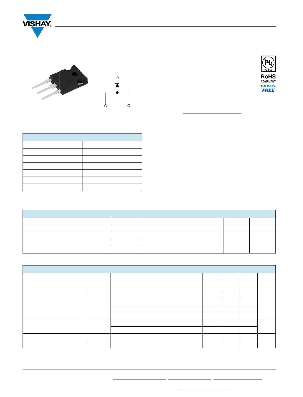
VS-60APH03-N3
Vishay Semiconductors
Hyperfast Rectifier, 60 A FRED Pt
PRIMARY CHARACTERISTICS
I
F(AV)
V
R
V
at I
F
F
t
typ. 28 ns
rr
max. 175 °C
T
J
Package TO-247AC 3L
Circuit configuration Single
60 A
300 V
0.85 V
®
FEATURES
• Hyperfast recovery time
• Low forward voltage drop
• Low leakage current
• Soft recovery device
• 175 °C operating junction temperature
• Designed and qualified according to JEDEC
• Material categorization: for definitions of compliance
please see www.vishay.com/doc?99912
DESCRIPTION / APPLICATIONS
VS-60APH03-N3 series are the state of the art ultrafast
recovery rectifiers designed with optimized performance of
forward voltage drop and ultrafast recovery time.
The planar structure and the platinum doped life time control
guarantee the best overall performance, ruggedness and
reliability characteristics.
These devices are intended for PDP and use in the output
rectification stage for SMPS, UPS, DC/DC converters as
well as freewheeling diodes in low voltage inverters.
Their extremely optimized stored charge and low recovery
current minimize the switching losses and reduce over
dissipation in the switching element and snubbers.
®
-JESD 47
ABSOLUTE MAXIMUM RATINGS
PARAMETER SYMBOL TEST CONDITIONS VALUES UNITS
Cathode to anode voltage V
Continuous forward current I
Single pulse forward current I
Operating junction and storage temperatures T
J
F(AV)
FSM
, T
R
TC = 103 °C 60
TJ = 25 °C, tp = 10 ms 450
Stg
300 V
-55 to +175 °C
ELECTRICAL SPECIFICATIONS (TJ = 25 °C unless otherwise specified)
PARAMETER SYMBOL TEST CONDITIONS MIN. TYP. MAX. UNITS
Breakdown voltage,
blocking voltage
Forward voltage V
Reverse leakage current I
Junction capacitance C
Series inductance L
Revision: 09-Oct-2019
For technical questions within your region: [email protected]
THIS DOCUMENT IS SUBJECT TO CHANGE WITHOUT NOTICE. THE PRODUCTS DESCRIBED HEREIN AND THIS DOCUMENT
ARE SUBJECT TO SPECIFIC DISCLAIMERS, SET FORTH AT www.vishay.com/doc?91000
,
V
BR
V
R
IR = 100 μA 300 - -
R
IF = 30 A - 1.0 1.25
I
= 60 A - - 1.45
F
T
S
F
= 30 A, TJ = 125 °C - 0.85 1.10
I
F
I
= 60 A, TJ = 125 °C - - 1.30
F
VR = VR rated - - 10
T
= 125 °C, VR = VR rated - - 100
J
VR = 300 V - 70 - pF
Measured lead to lead 5 mm from package body - 3.5 - nH
1
Document Number: 94796
A
V
μA
Page 2
VS-60APH03-N3
www.vishay.com
DYNAMIC RECOVERY CHARACTERISTICS (TJ = 25 °C unless otherwise specified)
PARAMETER SYMBOL TEST CONDITIONS MIN. TYP. MAX. UNITS
IF = 1.0 A, dIF/dt = 100 A/μs, VR = 30 V - 28 -
= 1.0 A, dIF/dt = 50 A/μs, VR = 30 V - 34 -
I
Reverse recovery time t
Peak recovery current I
Reverse recovery charge Q
rr
RRM
rr
F
= 25 °C
T
J
T
= 125 °C - 64 -
J
= 60 A
I
TJ = 25 °C - 3.0 -
T
= 125 °C - 8.5 -
J
F
dI
/dt = 200 A/μs
F
V
= 200 V
R
TJ = 25 °C - 65 -
T
= 125 °C - 273 -
J
THERMAL - MECHANICAL SPECIFICATIONS
PARAMETER SYMBOL TEST CONDITIONS MIN. TYP. MAX. UNITS
Maximum junction and
storage temperature range
Thermal resistance,
junction to case
Thermal resistance,
junction to ambient
Typical thermal resistance,
case to heatsink
Approximate Weight
Mounting torque
Marking device Case style TO-247AC 60APH03
T
, T
J
Stg
R
thJC
R
thJA
R
thCS
Typical socket mount - - 40
Mounting surface, flat, smooth, and greased - 0.4 -
Vishay Semiconductors
-42-
-55 - 175 °C
- 0.56 0.80
-6.0- g
-0.22- oz.
6.0 - 12 kgf. cm
(12) - (10) (lbf.in)
ns
A
nC
°C/W
1000
100
- Instantaneous Forward Current (A)
F
I
TJ = 175 °C
10
TJ = 25 °C
1
0.3 0.6 0.9 1.2 1.5
V
Forward Voltage Drop (V)
FM -
TJ = 125 °C
1000
100
10
1
0.1
- Reverse Current (μA)
0.01
R
I
0.001
175 °C
50 100 150 200 250 300
VR - Reverse Voltage (V)
150 °C
125 °C
100 °C
75 °C
50 °C
25 °C
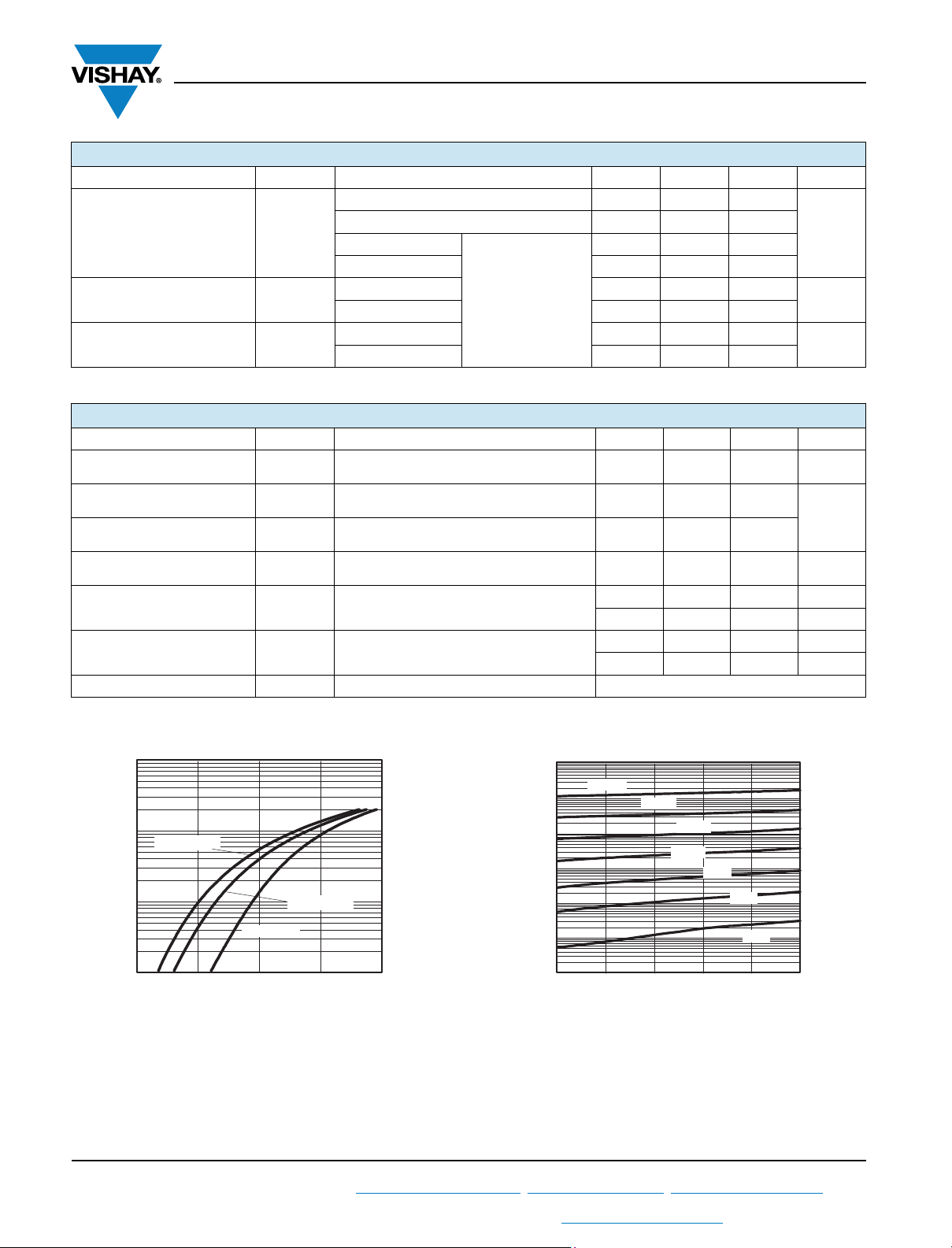
Fig. 1 - Typical Forward Voltage Drop Characteristics Fig. 2 - Typical Values of Reverse Current vs. Reverse Voltage
Revision: 09-Oct-2019
For technical questions within your region: [email protected]
THIS DOCUMENT IS SUBJECT TO CHANGE WITHOUT NOTICE. THE PRODUCTS DESCRIBED HEREIN AND THIS DOCUMENT
ARE SUBJECT TO SPECIFIC DISCLAIMERS, SET FORTH AT www.vishay.com/doc?91000
2
Document Number: 94796
Page 3
0 50 100 150 200 250 300
10
100
1000
VR - Reverse Voltage (V)
C
T
- Junction Capacitance (pF)
0
10
20
30
40
50 60 70
80 90
60
40
80
100
120
140
160
180
DC
Allowable Case Temperature (°C)
I
F(AV) -
Average Forward Current (A)
Average Power Loss (W)
I
F(AV) -
Average Forward Current (A)
0 10 20 30 40 50 60 70 80 90
0
20
40
60
80
100
120
D = 0.01
D = 0.02
D = 0.05
D = 0.1
D = 0.2
D = 0.5
DC
RMS Limit
www.vishay.com
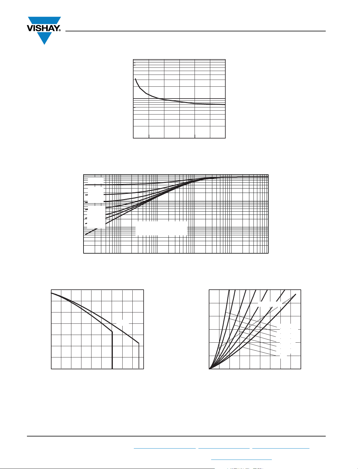
Fig. 3 - Typical Junction Capacitance vs. Reverse Voltage
1
D = 0.5
D = 0.2
D = 0.1
0.1
D = 0.05
D = 0.02
D = 0.01
0.01
- Thermal Impedance (°C/W)
thJC
Z
0.001
1E-05 1E-04 1E-03 1E-02 1E-01 1E+00
Fig. 4 - Maximum Thermal Impedance Z
Single Pulse
(Thermal Resistance)
t1 - Rectangular Pulse Duration (s)
Characteristics
thJC
VS-60APH03-N3
Vishay Semiconductors
Revision: 09-Oct-2019
Fig. 5 - Maximum Allowable Case Temperature
vs. Average Forward Current
For technical questions within your region: [email protected]
THIS DOCUMENT IS SUBJECT TO CHANGE WITHOUT NOTICE. THE PRODUCTS DESCRIBED HEREIN AND THIS DOCUMENT
Fig. 6 - Forward Power Loss Characteristics
3
ARE SUBJECT TO SPECIFIC DISCLAIMERS, SET FORTH AT www.vishay.com/doc?91000
Document Number: 94796
Page 4
t
rr
(ns)
dIF/dt (A/μs)
0001001
10
20
30
40
50
60
70
80
90
IF = 60 A, 25 °C
typical value
IF = 60 A, 125 °C
0001001
100
0
200
300
400
500
600
700
800
900
IF = 60 A, 25 °C
typical value
IF = 60 A, 125 °C
Q
rr
(nC)
dIF/dt (A/μs)
Q
rr
0.5 I
RRM
di
(rec)M
/dt
0.75 I
RRM
I
RRM
t
rr
t
b
t
a
I
F
diF/dt
0
(1)
(2)
(3)
(4)
(5)
(1) di
F
/dt - rate of change of current
through zero crossing
(2) I
RRM
- peak reverse recovery current
(3) t
rr
- reverse recovery time measured
from zero crossing point of negative
going I
F
to point where a line passing
through 0.75 I
RRM
and 0.50 I
RRM
extrapolated to zero current.
(4) Q
rr
- area under curve dened by t
rr
and I
RRM
trr x I
RRM
2
Qrr =
(5) di
(rec)M
/dt - peak rate of change of
current during t
b
portion of t
rr
VS-60APH03-N3
www.vishay.com
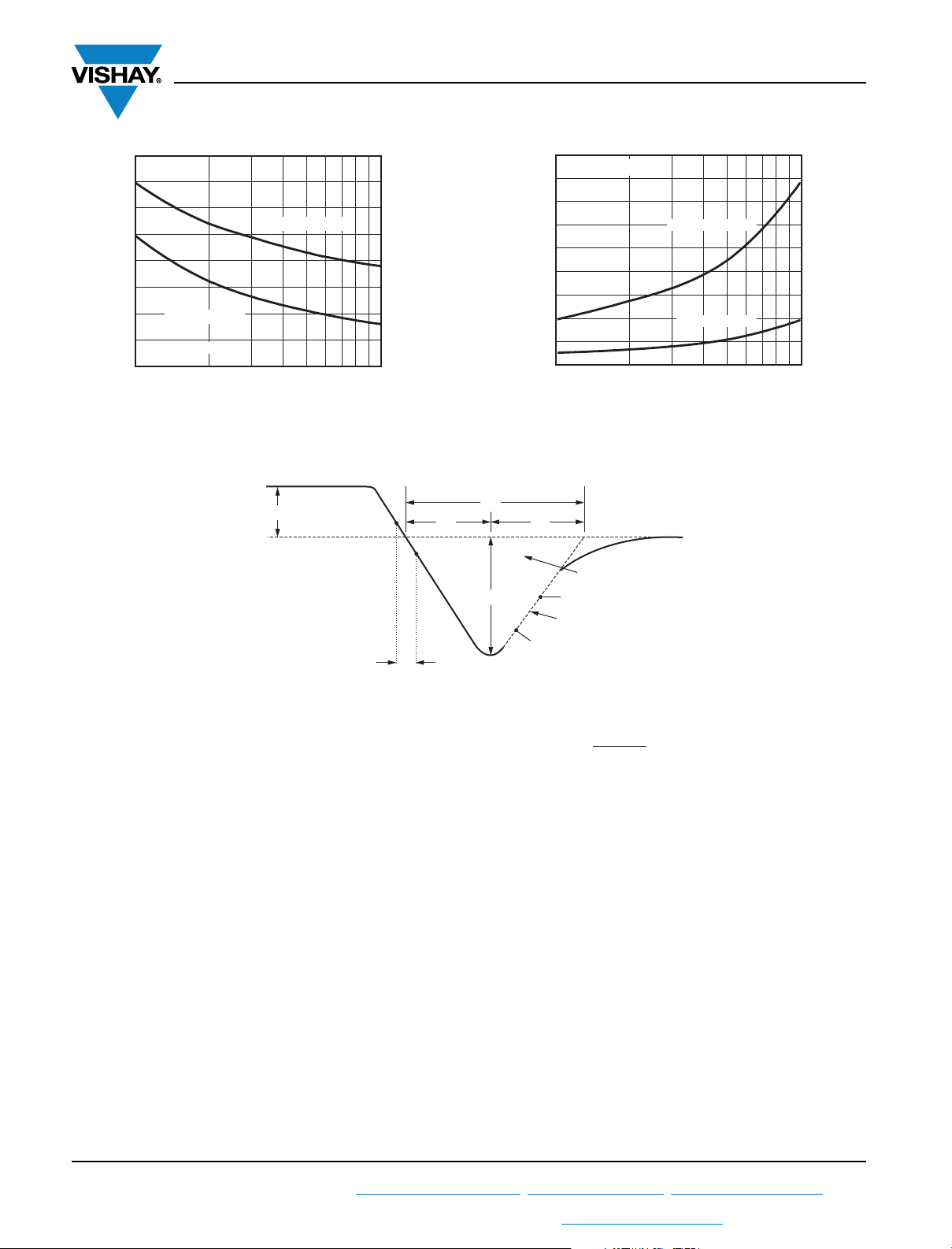
Fig. 7 - Typical Reverse Recovery vs. dIF/dt Fig. 8 - Typical Stored Charge vs. dIF/dt
Vishay Semiconductors
Revision: 09-Oct-2019
For technical questions within your region: [email protected]
THIS DOCUMENT IS SUBJECT TO CHANGE WITHOUT NOTICE. THE PRODUCTS DESCRIBED HEREIN AND THIS DOCUMENT
Fig. 9 - Reverse Recovery Waveform and Definitions
ARE SUBJECT TO SPECIFIC DISCLAIMERS, SET FORTH AT www.vishay.com/doc?91000
4
Document Number: 94796
Page 5
www.vishay.com
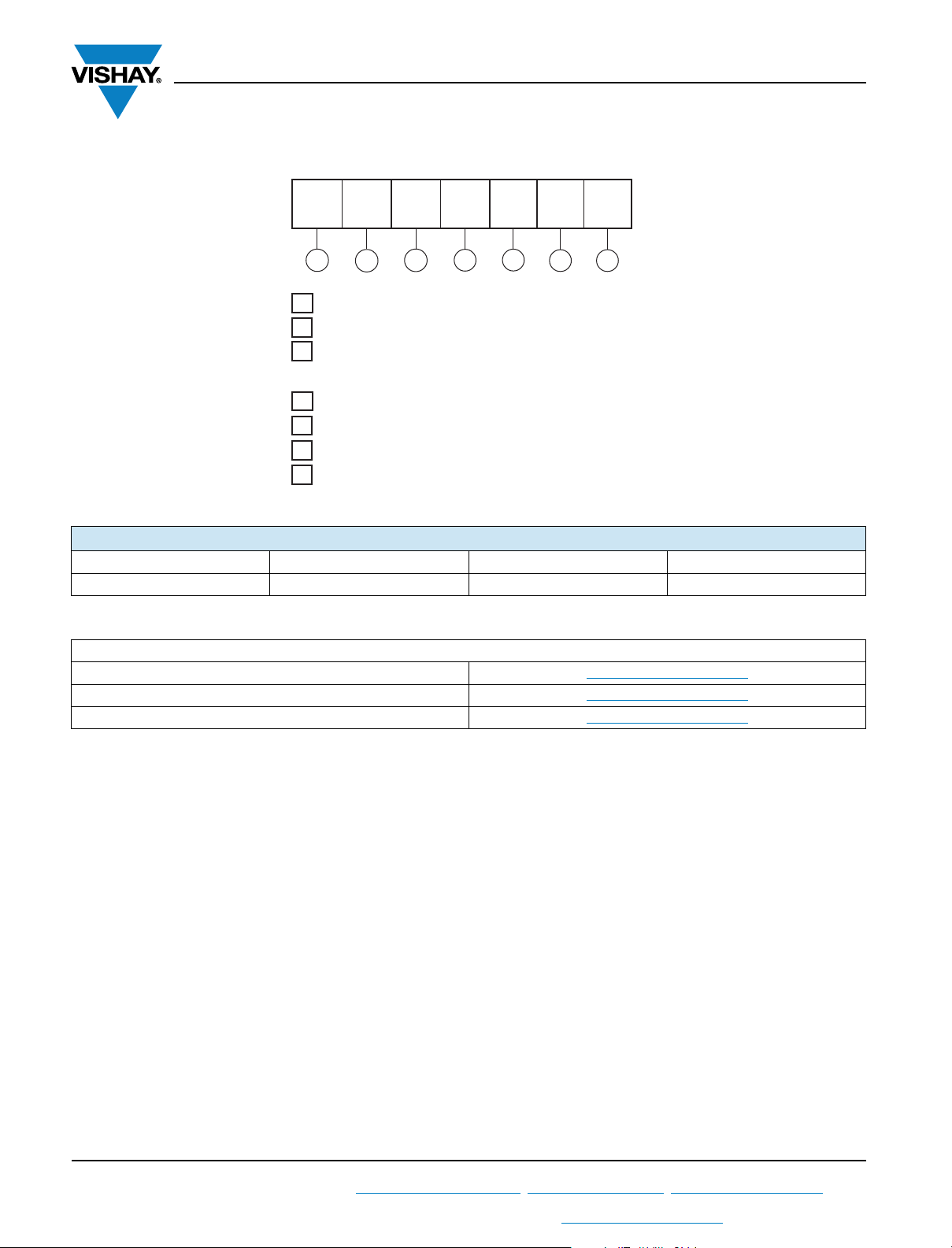
2 - Current rating (60 = 60 A)
3 - Circuit configuration:
4 - P = TO-247 AC
5
-
H = hyperfast rectifier
6
- Voltage code (03 = 300 V)
- -N3 = halogen-free, RoHS-compliant, and totally lead (Pb)-free
7
Device code
51 32 4 6 7
VS- 60 A P H 03 -N3
1 - Vishay Semiconductors product
A = single diode, 3 pins
ORDERING INFORMATION TABLE
VS-60APH03-N3
Vishay Semiconductors
ORDERING INFORMATION (Example)
PREFERRED P/N QUANTITY PER TUBE MINIMUM ORDER QUANTITY PACKAGING DESCRIPTION
VS-60APH03-N3 25 500 Antistatic plastic tube
LINKS TO RELATED DOCUMENTS
Dimensions www.vishay.com/doc?96138
Part marking information www.vishay.com/doc?95007
SPICE model www.vishay.com/doc?96075
Revision: 09-Oct-2019
For technical questions within your region: [email protected]
THIS DOCUMENT IS SUBJECT TO CHANGE WITHOUT NOTICE. THE PRODUCTS DESCRIBED HEREIN AND THIS DOCUMENT
ARE SUBJECT TO SPECIFIC DISCLAIMERS, SET FORTH AT www.vishay.com/doc?91000
5
Document Number: 94796
 Loading...