

Page 1
VRE305
Low Cost
Precision Reference
THALER CORPORATION • 2015 N. FORBES BOULEVARD • TUCSON, AZ. 85745 • (520) 882-4000
FEATURES
• 5.000 V OUTPUT ± 0.500 mV (.01%)
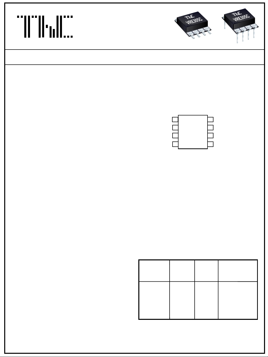
PIN CONFIGURATION
• TEMPERATURE DRIFT: 0.6 ppm/°C
NOISE
µV
• LOW NOISE: 3
(0.1-10Hz)
p-p
• INDUSTRY STD PINOUT- 8 PIN DIP OR
SURFACE MOUNT PACKAGE
•EXCELLENT LINE REGULATION: 6ppm/V Typ.
N/C
+V
IN
TEMP
GND
1
2
3
4
VRE305
TOP
VIEW
8
7
6
5
REDUCTION
REF. GND
V
OUT
TRIM
• OUTPUT TRIM CAPABILITY
DESCRIPTION
The VRE305 is a low cost, high precision 5.0V
reference. Packaged in the industry standard 8
pin DIP, the device is ideal for upgrading systems
that use lower performance references.
The device provides ultrastable +5.000V output
with ±0.5000 mV (.01%) initial accuracy and a
temperature coefficient of 0.6 ppm/°C. This
improvement in accuracy is made possible by a
unique, patented multipoint laser compensation
technique developed by Thaler Corporation.
Significant improvements have been made in
other performance parameters as well, including
initial accuracy, warm-up drift, line regulation, and
long-term stability, making the VRE305 series the
most accurate reference available in the standard
8 pin DIP package.
For enhanced performance, the VRE305 has an
external trim option for users who want less than
0.01% initial error. For ultra low noise
applications, an external capacitor can be
attached between the noise reduction pin and the
ground pin. A reference ground pin is provided to
eliminate socket contact resistance errors.
FIGURE 1
The VRE305 is recommended for use as a
reference for 14, 16, or 18 bit D/A converters
which require an external precision reference.
The device is also ideal for calibrating scale factor
on high resolution A/D converters. The VRE305
offers superior performance over monolithic
references.
SELECTION GUIDE
Initial
Error
Model
VRE305A 0.5 0.6 0°C to +70°C
VRE305B 0.8 1.0 0°C to +70°C
VRE305C 1.0 2.0 0°C to +70°C
VRE305J 0.5 0.6 -40°C to +85°C
VRE305K 0.8 1.0 -40°C to +85°C
VRE305L 1.0 2.0 -40°C to +85°C
For package option add D for DIP or S for Surface Mount
to end of model number.
mV
Temp.
Coeff.
ppm/°C
Temp.
Range
°C
VRE305DS REV. D MAY 2001
Page 2
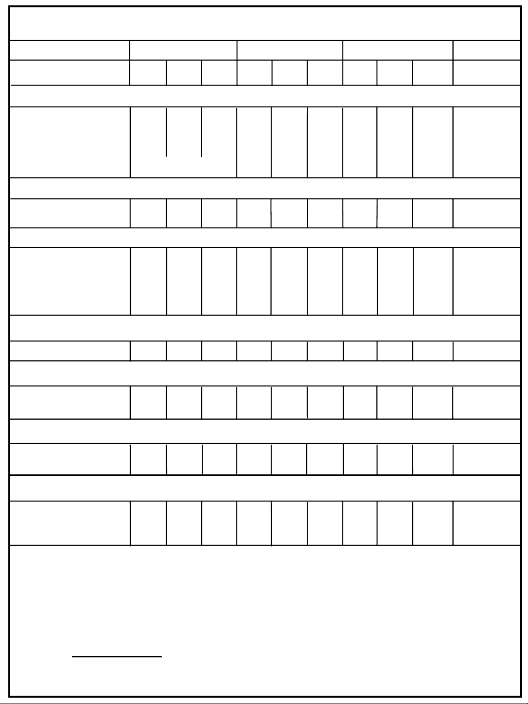
ELECTRICAL SPECIFICATIONS
Vps =+15V, T = 25°C, RL = 10kΩ unless otherwise noted.
MODEL A/J B/K C/L
VRE305
PARAMETER
MIN TYP MAX MIN TYP MAX MIN TYP MAX UNITS
ABSOLUTE RATINGS
Power Supply +13.5+15+22****** V
Operating Temp. (
Operating Temp. (
A,B,C)0 +70 * * * * °C
J,K,L)-40 +85 * * * * °C
Storage Temperature -65 +150 * * * * °C
Short Circuit Protection Continuous * *
OUTPUT VOLTAGE
VRE305 5.000 * * V
(1)
Temp. Sensor Voltage 630 * * mV
OUTPUT VOLTAGE ERRORS
Initial Error 0.50 0.80 1.00 mV
(2)
Warmup Drift 1 2 3 ppm
T
min-Tmax
(3)
0.6 1.0 2.0 ppm/°C
Long-Term Stability 6 * * ppm/1000hrs
Noise (.1-10Hz) 3 * * µVpp
(4)
OUTPUT CURRENT
Range ±10 * * mA
REGULATION
Line 6 10 * * * * ppm/V
Load 3 * * ppm/mA
OUTPUT ADJUSTMENT
Range 10 * * mV
POWER SUPPLY CURRENTS
(5)
VRE305 +PS 5 7 * * * * mA
NOTES: *Same as A/J Models.
1. The temp. reference TC is 2.1mV/°C
2. The specified values are without external trim.
4. The specified values are without the external
noise reduction capacitor.
5. The specified values are unloaded.
3. The temperature coefficient is determined by the box
method using the following formula:
V
max-Vmin
T.C. = x 10
V
nominal
x (T
max-Tmin
)
6
VRE305DS REV. D MAY 2001
Page 3
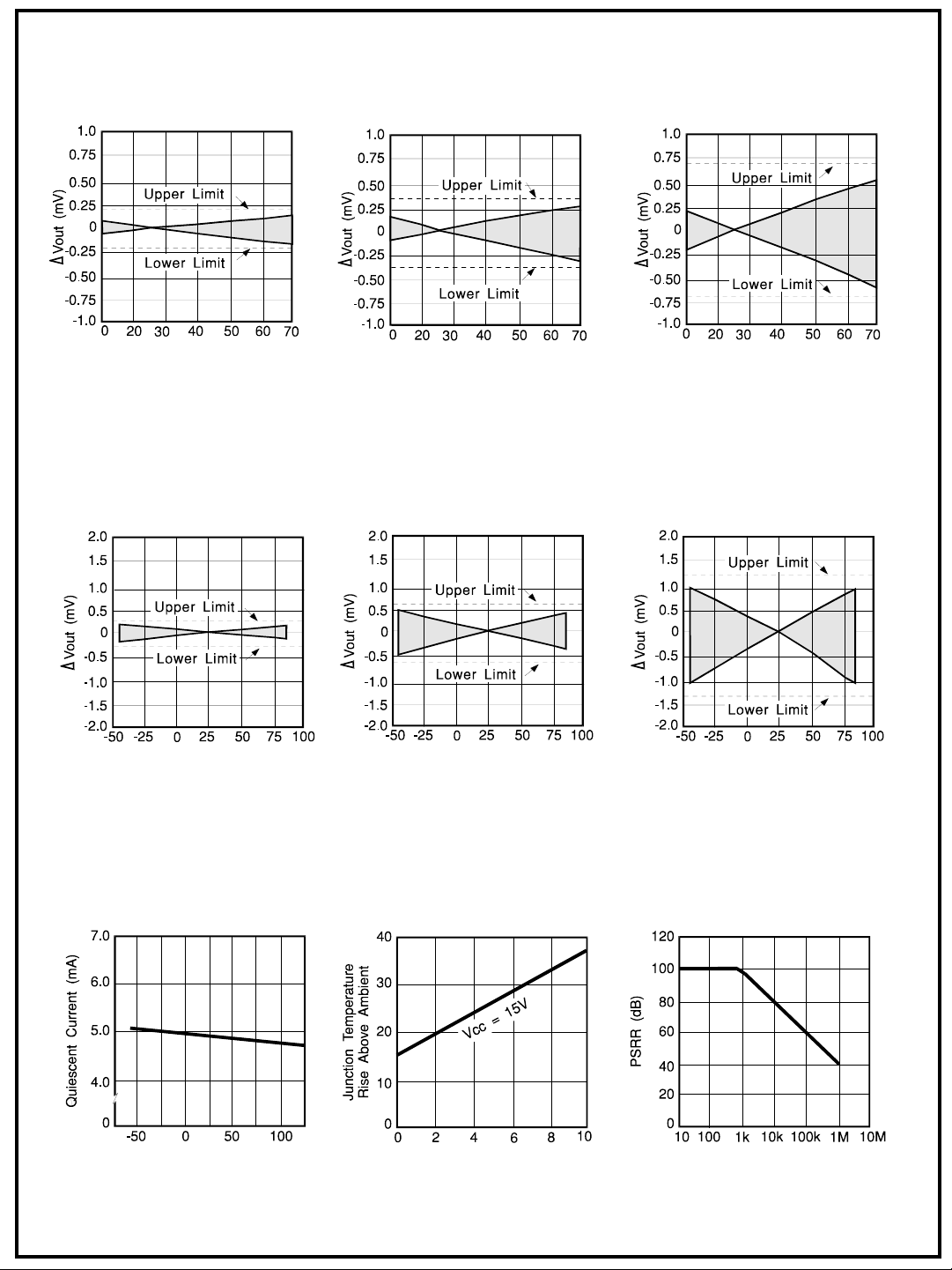
vs. TEMPERATURE
V
OUT
TYPICAL PERFORMANCE CURVES
V
vs. TEMPERATURE
OUT
V
OUT
vs. TEMPERATURE
TemperatureoC
VRE305A
vs. TEMPERATURE
V
OUT
TemperatureoC
VRE305J
Temperature
VRE305B
vs. TEMPERATURE
V
OUT
TemperatureoC
VRE305K
o
C
TemperatureoC
VRE305C
vs. TEMPERATURE
V
OUT
Temperature
o
C
VRE305L
QUIESCENT CURRENT VS. TEMP
TemperatureoC
JUNCTION TEMP. RISE VS. OUTPUT CURRENT
Output Current (mA)
PSRR VS. FREQUENCY
Frequency (Hz)
VRE305DS REV. D MAY 2001
Page 4
DISCUSSION OF PERFORMANCE
THEORY OF OPERATION
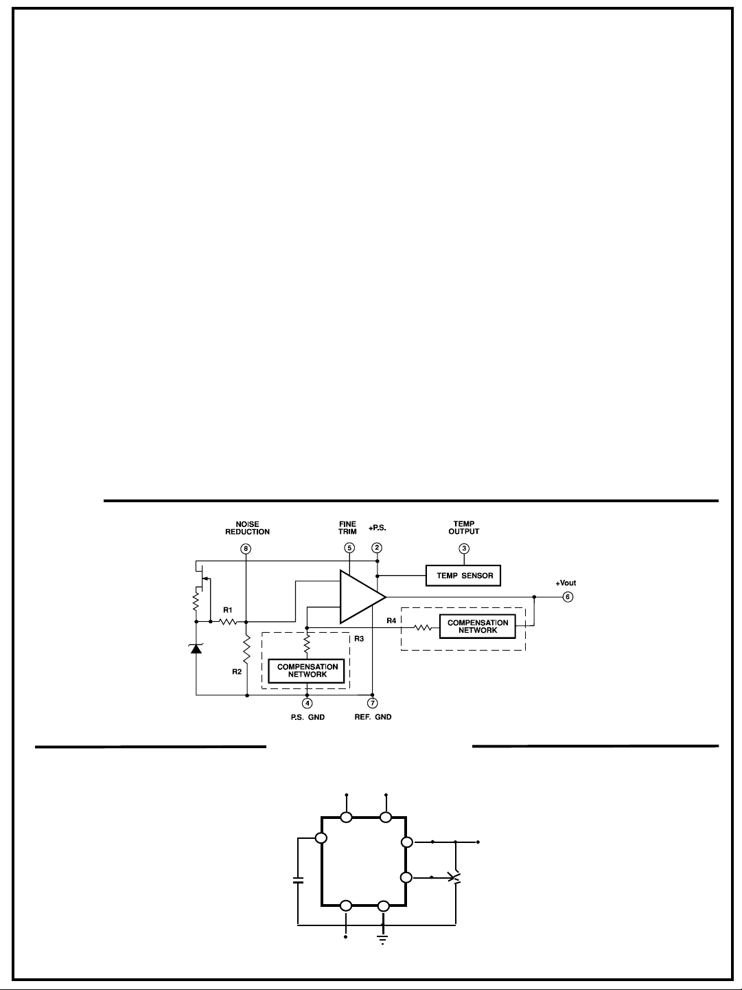
The following discussion refers to the schematic in
figure 2 below. A FET current source is used to bias a
6.3V zener diode. The zener voltage is divided by the
resistor network R1 and R2. This voltage is then applied
to the noninverting input of the operational amplifier which
amplifies the voltage to produce a 5.000V output. The
gain is determined by the resistor networks R3 and R4:
G=1 + R4/R3. The 6.3V zener diode is used because it is
the most stable diode over time and temperature.
The current source provides a closely regulated zener
current, which determines the slope of the references’
voltage vs. temperature function. By trimming the zener
current a lower drift over temperature can be achieved.
But since the voltage vs. temperature function is nonlinear
this compensation technique is not well suited for wide
temperature ranges.
Thaler Corporation has developed a nonlinear
compensation network of thermistors and resistors that is
used in the VRE series voltage references. This
proprietary network eliminates most of the nonlinearity in
the voltage vs. temperature function. By adjusting the
slope, Thaler Corporation produces a very stable voltage
over wide temperature ranges.
This network is less than 2% of the overall network
resistance so it has a negligible effect on long term
stability.
Figure 3 shows the proper connection of the VRE305
series voltage references with the optional trim resistor for
initial error and the optional capacitor for noise reduction.
The VRE305 reference has the ground terminal brought
out on two pins (pin 4 and pin 7) which are connected
together internally. This allows the user to achieve greater
accuracy when using a socket. Voltage references have a
voltage drop across their power supply ground pin due to
quiescent current flowing through the contact resistance.
If the contact resistance was constant with time and
temperature, this voltage drop could be trimmed out.
When the reference is plugged into a socket, this source
of error can be as high as 20ppm. By connecting pin 4 to
the power supply ground and pin 7 to a high impedance
ground point in the measurement circuit, the error due to
the contact resistance can be eliminated. If the unit is
soldered into place, the contact resistance is sufficiently
small that it does not effect performance. Pay careful
attention to the circuit layout to avoid noise pickup and
voltage drops in the lines.
VRE305
FIGURE 2
OPTIONAL
NOISE REDUCTION
CAPACITOR
EXTERNAL CONNECTIONS
C
N
1µF
+ V
8
VRE305
2
7
IN
V TEMP OUT
3
6
5
4
10K
+ V
OUT
OPTIONAL
Ω
FINE TRIM
ADJUSTMENT
FIGURE 3
REF. GND
VRE305DS REV. D MAY 2001
Page 5
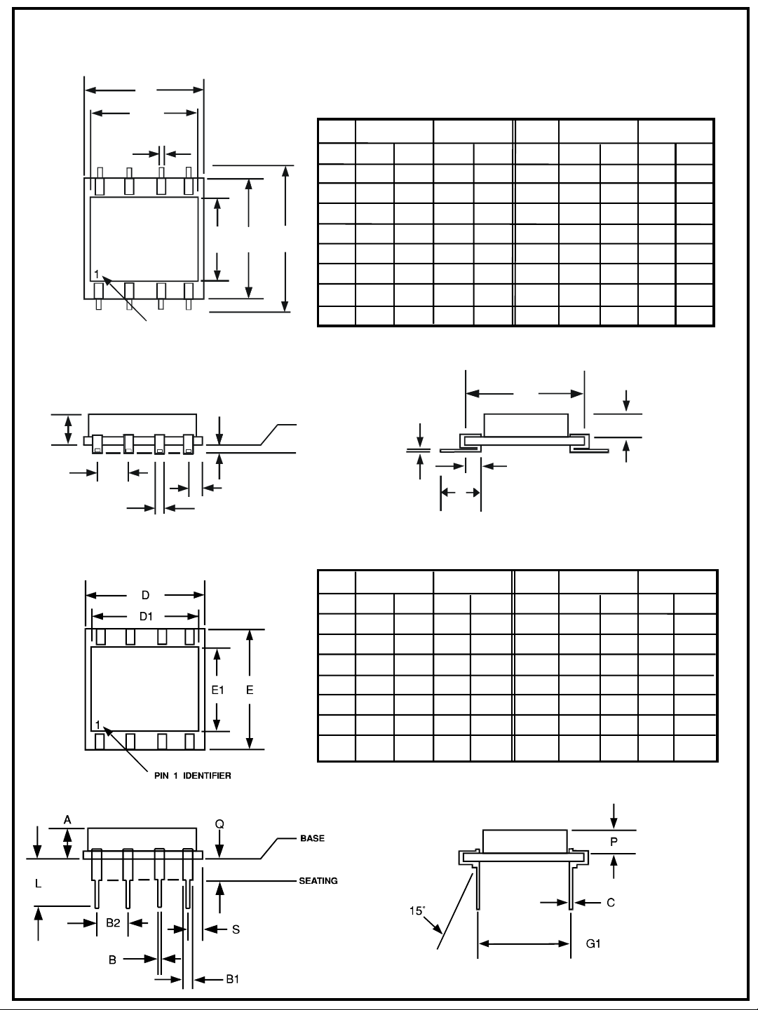
FIGURE 3
A
Q
D
D1
D2
PIN 1 IDENTIFIER
E2
E1
MECHANICAL
INCHES MILLIMETER
DIM MIN MAX MIN MAX DIM MIN MAX MIN MAX
A .115 .125 2.92 3.17 D2 .018 .023 0.46 0.58
B .098 .102 2.48 2.59 E .507 .513 12.8 13.0
B1 .046 .051 1.14 1.29 E1 .397 .403 10.0 10.2
E
C .107 .113 2.71 2.89 E2 .264 .270 6.70 6.85
C1 .009 .012 0.22 0.30 P .085 .095 2.15 2.41
C2 .052 .058 1.32 1.47 Q .020 .030 .508 .762
D .397 .403 10.0 10.2 S .045 .055 1.14 1.39
D1 .372 .380 9.44 9.65
INCHES MILLIMETER
E1
B
FIGURE 4
B1
BASE
SEATING
C1
P
C2
S
INCHES MILLIMETER
DIM MIN MAX MIN MAX DIM MIN MAX MIN MAX
A .115 .125 2.92 3.17 E .397 .403 10.0 10.2
B .018 .022 .457 .558 E1 .264 .270 6.70 6.85
B1 .046 .051 1.14 1.29 G1 .290 .310 7.36 7.87
B2 .098 .102 2.48 2.59 L .195 .215 4.95 5.46
C .009 .012 0.22 0.30 P .085 .095 2.15 2.41
D .397 .403 10.0 10.2 Q .055 .065 1.39 1.65
D 1 .372 .380 9.44 9.65 S .045 .055 1.14 1.39
C
INCHES MILLIMETER
VRE305DS REV. D MAY 2001
 Loading...