

Page 1
VPX 3225D,
VPX 3224D
Video Pixel Decoders
Edition Nov. 9, 1998
6251-432-2PD
PRELIMINARY DATA SHEET
MICRONAS
MICRONAS
Page 2

VPX 3225D, VPX 3224D
Contents
Page Section Title
6 1. Introduction
7 1.1. System Architecture
8 2. Functional Description
8 2.1. Analog Front-End
8 2.1.1. Input Selector
8 2.1.2. Clamping
8 2.1.3. Automatic Gain Control
8 2.1.4. Analog-to-Digital Converters
8 2.1.5. ADC Range
8 2.1.6. Digitally Controlled Clock Oscillator
10 2.2. Color Decoder
10 2.2.1. IF-Compensation
10 2.2.2. Demodulator
11 2.2.3. Chrominance Filter
11 2.2.4. Frequency Demodulator
1 1 2.2.5. Burst Detection
11 2.2.6. Color Killer Operation
11 2.2.7. PAL Compensation/1-H Comb Filter
12 2.2.8. Luminance Notch Filter
13 2.3. Video Sync Processing
13 2.4. Macrovision Detection (version D4 only)
14 2.5. Component Processing
15 2.5.1. Horizontal Resizer
16 2.5.2. Skew Correction
16 2.5.3. Peaking and Coring
16 2.5.4. YCbCr Color Space
16 2.5.5. Video Adjustments
17 2.6. Video Output Interface
17 2.6.1. Output Formats
17 2.6.1.1. YUV 4:2:2 with Separate Syncs/ITU-R601
18 2.6.1.2. Embedded Reference Headers/ITU-R656
20 2.6.1.3. Embedded Timing Codes (BStream)
20 2.6.2. Bus Shuffler
20 2.6.3. Output Multiplexer
20 2.6.4. Output Ports
21 2.7. Video Data Transfer
21 2.7.1. Single and Double Clock Mode
22 2.7.2. Half Clock Mode
23 2.8. Video Reference Signals
23 2.8.1. HREF
23 2.8.2. VREF
23 2.8.3. Odd/Even Information (FIELD)
25 2.8.4. VACT
PRELIMINARY DATA SHEET
2 Micronas
Page 3

PRELIMINARY DATA SHEET
Contents, continued
Page Section Title
26 2.9. Operational Modes
26 2.9.1. Open Mode
26 2.9.2. Scan Mode
28 2.10. Windowing the Video Field
29 2.11. Temporal Decimation
30 2.12. Data Slicer
30 2.12.1. Slicer Features
30 2.12.2. Data Broadcast Systems
31 2.12.3. Slicer Functions
31 2.12.3.1. Input
31 2.12.3.2. Automatic Adaptation
31 2.12.3.3. Standard Selection
31 2.12.3.4. Output
33 2.13. VBI Data Acquisition
33 2.13.1. Raw VBI Data
34 2.13.2. Sliced VBI Data
35 2.14. Control Interface
35 2.14.1. Overview
35 2.14.2. I
35 2.14.3. Reset and I
35 2.14.4. Protocol Description
36 2.14.5. FP Control and Status Registers
37 2.15. Initialization of the VPX
37 2.15.1. Power-on-Reset
37 2.15.2. Software Reset
37 2.15.3. Low Power Mode
38 2.16. JTAG Boundary-Scan, Test Access Port (TAP)
38 2.16.1. General Description
38 2.16.2. T AP Architecture
38 2.16.2.1. T AP Controller
38 2.16.2.2. Instruction Register
38 2.16.2.3. Boundary Scan Register
39 2.16.2.4. Bypass Register
39 2.16.2.5. Device Identification Register
39 2.16.2.6. Master Mode Data Register
39 2.16.3. Exception to IEEE 1149.1
39 2.16.4. IEEE 1 149.1–1990 Spec Adherence
39 2.16.4.1. Instruction Register
39 2.16.4.2. Public Instructions
40 2.16.4.3. Self-Test Operation
40 2.16.4.4. Test Data Registers
40 2.16.4.5. Boundary-Scan Register
40 2.16.4.6. Device Identification Register
40 2.16.4.7. Performance
44 2.17. Enable/Disable of Output Signals
2
C-Bus Interface
2
C Device Address Selection
VPX 3225D, VPX 3224D
3Micronas
Page 4

VPX 3225D, VPX 3224D
Contents, continued
Page Section Title
45 3. Specifications
45 3.1. Outline Dimensions
48 3.2. Pin Connections and Short Descriptions
45 3.3. Pin Descriptions
47 3.4. Pin Configuration
48 3.5. Pin Circuits
50 4. Electrical Characteristics
50 4.1. Absolute Maximum Ratings
51 4.2. Recommended Operating Conditions
51 4.2.1. Recommended Analog Video Input Conditions
52 4.2.2. Recommended I
52 4.2.3. Recommended Digital Inputs Levels of RES, OE, TCK, TMS, TDI
53 4.2.4. Recommended Crystal Characteristics
54 4.3. Characteristics
54 4.3.1. Current Consumption
54 4.3.2. Characteristics, Reset
54 4.3.3. XTAL Input Characteristics
55 4.3.4. Characteristics, Analog Front-End and ADCs
56 4.3.5. Characteristics, Control Bus Interface
56 4.3.6. Characteristics, JTAG Interface (Test Access Port TAP)
57 4.3.7. Characteristics, Digital Inputs/Outputs
57 4.3.8. Clock Signals PIXCLK, LLC, and LLC2
58 4.3.9. Digital Video Interface
58 4.3.10. Characteristics, TTL Output Driver
59 4.3.10.1. TTL Output Driver Description
2
C Conditions
PRELIMINARY DATA SHEET
60 5. Timing Diagrams
60 5.1. Power-up Sequence
60 5.2. Default Wake-up Selection
61 5.3. Control Bus Timing Diagram
62 5.4. Output Enable by Pin OE
63 5.5. Timing of the Test Access Port TAP
63 5.6. Timing of all Pins connected to the Boundary-Scan-Register-Chain
64 5.7. Timing Diagram of the Digital Video Interface
64 5.7.1. Characteristics, Clock Signals
65 6. Control and Status Registers
65 6.1. Overview
68 6.1.1. Description of I
72 6.1.2. Description of FP Control and Status Registers
2
C Control and Status Registers
4 Micronas
Page 5

PRELIMINARY DATA SHEET
Contents, continued
Page Section Title
83 7. Application Notes
83 7.1. Differences between VPX 3220A and VPX 322xD
83 7.2. Impact to Signal to Noise Ratio
83 7.3. Control Interface
83 7.3.1. Symbols
2
83 7.3.2. Write Data into I
83 7.3.3. Read Data from I
83 7.3.4. Write Data into FP Register
83 7.3.5. Read Data from FP Register
84 7.3.6. Sample Control Code
84 7.4. Xtal Supplier
85 7.5. Typical Application
88 8. Data Sheet History
C Register
2
C Register
VPX 3225D, VPX 3224D
5Micronas
Page 6

VPX 3225D, VPX 3224D
PRELIMINARY DATA SHEET
Video Pixel Decoder
Release Note: This data sheet describes functions
and characteristics of VPX 322xD–C3 and D4. Revision bars indicate significant changes to the previous edition.
1. Introduction
The Video Pixel Decoders VPX 3225D and VPX 3224D
are the second generation of full feature video acquisition ICs for consumer video and multimedia applications. All of the processing necessary to convert an analog video signal into a digital component stream have
been integrated onto a single 44-pin IC. Moreover, the
VPX 3225D provides text slicing for intercast, teletext,
and closed caption. Both chips are pin compatible to
VPX 3220A, VPX 3216B, and VPX 3214C. Notable features include:
Video Decoding
– multistandard color decoding:
• NTSC-M, NTSC-443
• P AL-BGHI, PAL-M, PAL-N, PAL-60
• SECAM
• S-VHS
– NTSC with Y/C comb filter
– two 8-bit video A/D converters with clamping and auto-
matic gain control (AGC)
– four analog inputs with integrated selector for:
• 3 composite video sources (CVBS), or
• 2 Y/C sources (S-VHS), or
• 2 composite video sources and one Y/C source.
– horizontal and vertical sync detection for all standards
– decodes and detects Macrovision 7.1 protected video
(version D4 only)
Video Processing
– hue, brightness, contrast, and saturation control
Video Interfacing
– YC
– ITU-R 601 compliant output format
– ITU-R 656 compliant output format
– BStream compliant output format
– square pixel format (640 or 768 pixel/line)
– 8-bit or 16-bit synchronous output mode
– 13.5 MHz/16-bit and 27 MHz/8-bit output rate
– VBI bypass and raw ADC data output
Data Broadcast Support (VPX 3225D only)
– high-performance data slicing in hardware
– multistandard data slicer
– full support for
– programmable to new standards via I2C
– automatic slice level adaptation
– VBI and Full-Field mode
– data insertion into video stream
– simultaneous acquisition of teletext, VPS, WSS, and
Miscellaneous
– 44-pin PLCC package
– total power consumption of below 1 W
– I
– single on-chip clock generation, only one crystal need-
– user programmable output pins
– power-down mode
4:2:2 format
bCr
• NABTS, WST
• CAPTION (1x,2x), VPS, WSS, Antiope
• teletext, intercast, wavetop,
• WebTV for windows, EPG services
caption
2
C serial control, 2 different device addresses
ed for all standards
– dual window cropping and scaling
– horizontal resizing between 32 and 864 pixels/line
– vertical resizing by line dropping
– high-quality anti-aliasing filter
– scaling controlled peaking and coring
6 Micronas
– IEEE 1149.1 (JTAG) boundary scan interface
Software Support
– MediaCVR Software Suite
• Video for Windows driver
• TV viewer applet, teletext browser
• intercast/wavetop browser
– WebTV for Windows
• Video capture and VBI services
Page 7
PRELIMINARY DATA SHEET
1.1. System Architecture
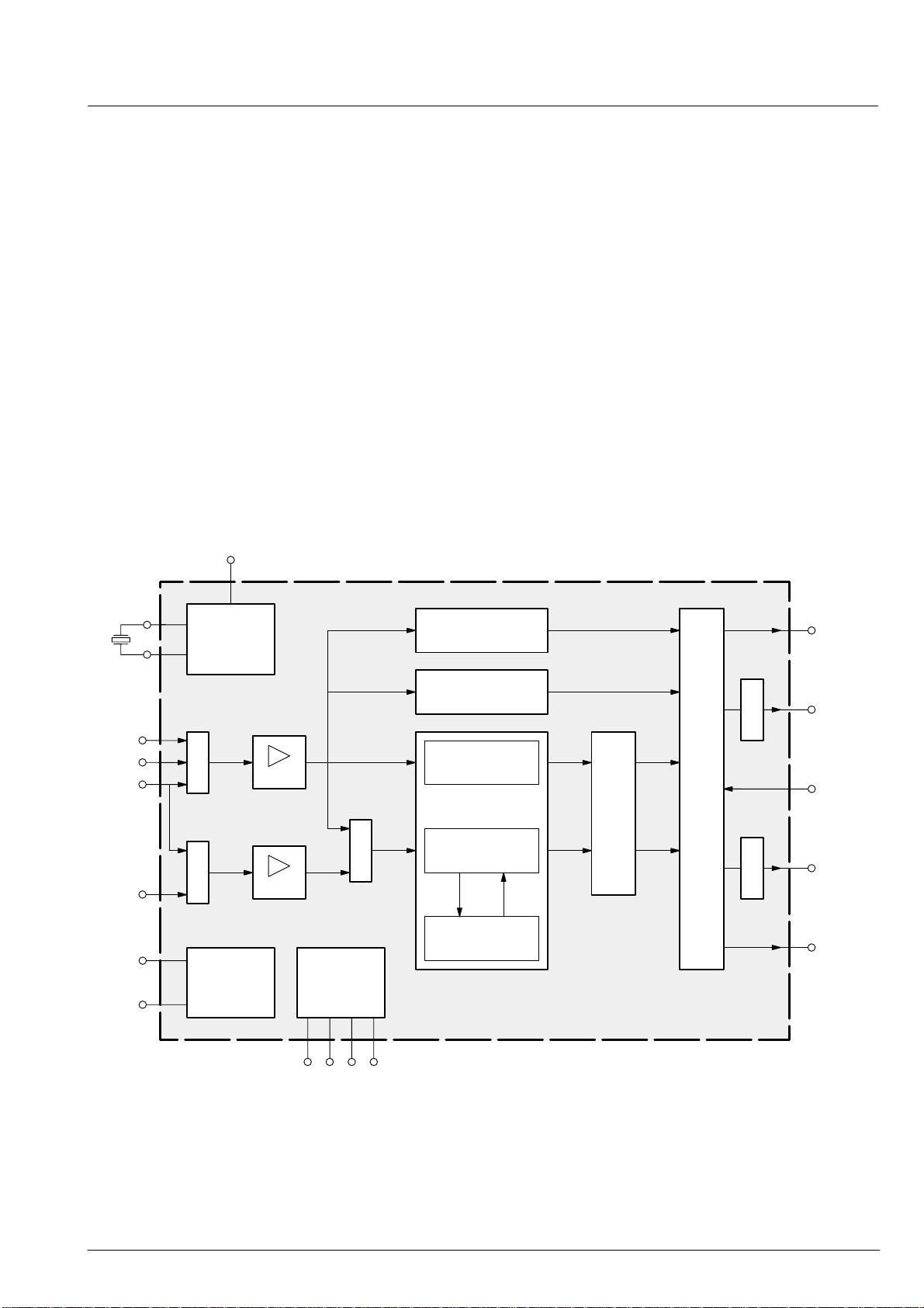
The block diagram (Fig. 1–1) illustrates the signal flow
through the VPX. A sampling stage performs 8-bit A/D
conversion, clamping, and AGC. The color decoder separates the luma and chroma signals, demodulates the
chroma, and filters the luminance. A sync slicer detects
the sync edge and computes the skew relative to the
sample clock. The video processing stage resizes the
YCbCr samples, adjusts the contrast and brightness,
and interpolates the chroma. The text slicer extracts
lines with text information and delivers decoded data
bytes to the video interface.
Note: The VPX 3225D and VPX 3224D are not register
compatible with the VPX 3220A, VPX 3216B, and
VPX 3214C family.
VPX 3225D, VPX 3224D
CVBS/Y
Chroma
SDA
SCL
RESQ
Clock Gen.
DCO
MUX
MUX
ADC
ADC
I2C JTAG
MUX
Sync Processing
Text Slicer
(VPX 3225D only)
Luma Filter
Video Decoder
Chroma
Demodulator
Line Store
YY
C
bCr
CbC
Video Processing
Video Interface
r
PortPort
HREF
VREF
FIELD
A[7:0]
OEQ
B[7:0]
PIXCLK
LLC
VACT
TDI
TMS
TDO
TCK
Fig. 1–1: Block diagram of the VPX 3224D, VPX 3225D
7Micronas
Page 8
VPX 3225D, VPX 3224D
PRELIMINARY DATA SHEET
2. Functional Description
The following sections provide an overview of the different functional blocks within the VPX. Most of them are
controlled by the Fast Processor (‘FP’) embedded in the
decoder. For controlling, there are two classes of regis-
2
ters: I
C registers (directly addressable via I2C bus) and
FP-RAM registers (ram memory of the FP; indirectly addressable via I
2
C bus). For further information, see sec-
tion 2.14.1.
2.1. Analog Front-End
This block provides the analog interfaces to all video inputs and mainly carries out analog-to-digital conversion
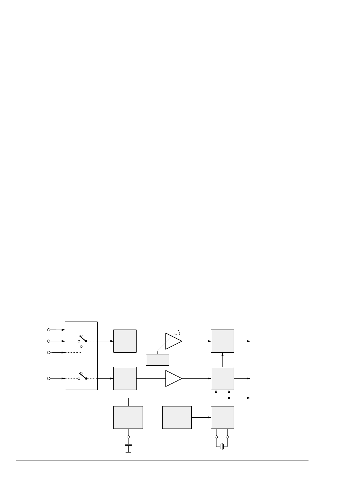
for the following digital video processing. A block diagram is given in Fig. 2–1.
Clamping, AGC, and clock DCO are digitally controlled.
The control loops are closed by the embedded processor.
2.1.1. Input Selector
Up to four analog inputs can be connected. Three inputs
(VIN1–3) are for input of composite video or S-VHS luma
signal. These inputs are clamped to the sync back porch
and are amplified by a variable gain amplifier. Two inputs, one dedicated (CIN) and one shared (VIN1), are
for connection of S-VHS carrier-chrominance signal.
The chrominance input is internally biased and has a
fixed gain amplifier.
pacitors and is generated by digitally controlled current
sources. The clamping level is the back porch of the video signal. S-VHS chroma is AC coupled. The input pin
is internally biased to the center of the ADC input range.
2.1.3. Automatic Gain Control
A digitally working automatic gain control adjusts the
magnitude of the selected baseband by +6/–4.5 dB in 64
logarithmic steps to the optimal range of the ADC. The
gain of the video input stage including the ADC is 213
steps/V with the AGC set to 0 dB.
2.1.4. Analog-to-Digital Converters
Two ADCs are provided to digitize the input signals.
Each converter runs with 20.25 MHz and has 8-bit resolution. An integrated bandgap circuit generates the required reference voltages for the converters. The two
ADCs are of a 2-stage subranging type.
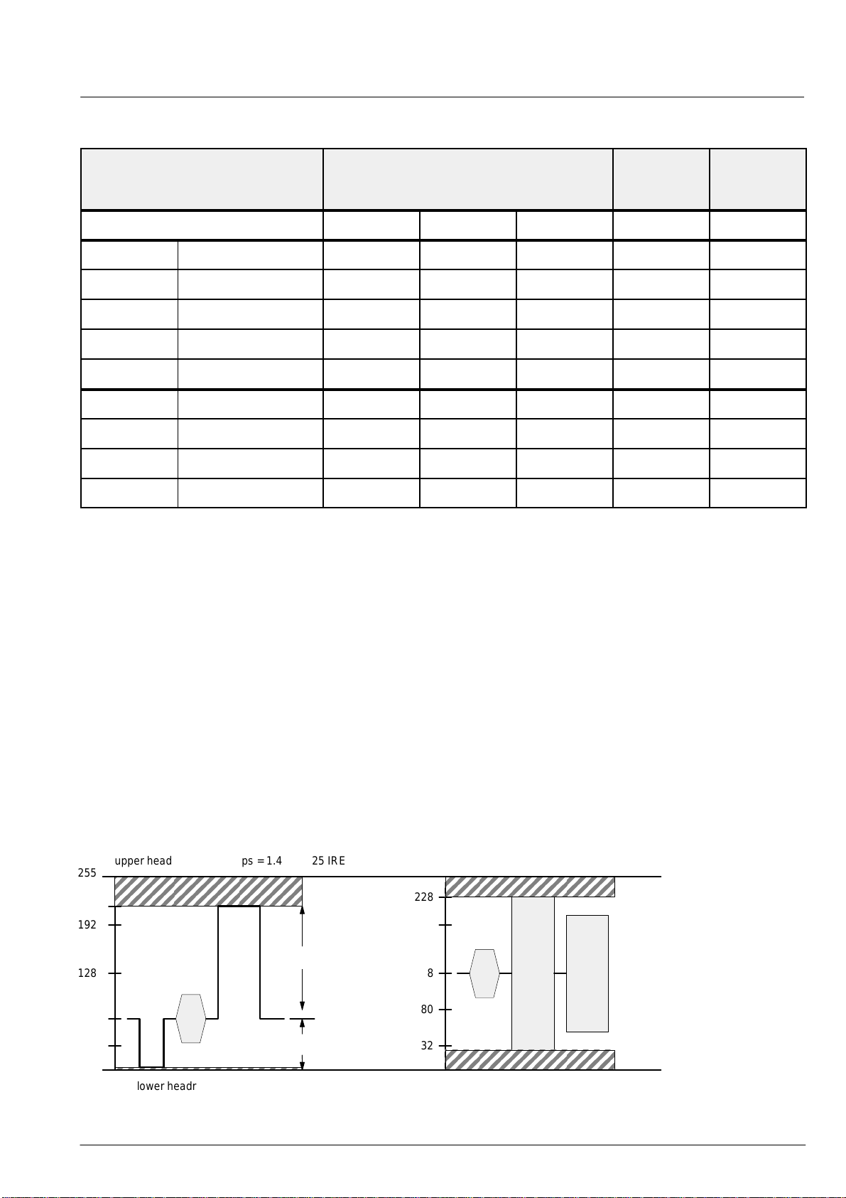
2.1.5. ADC Range
The ADC input range for the various input signals and
the digital representation is given in Table 2–1 and Fig.
2–2. The corresponding output signal levels of the
VPX 32xx are also shown.
2.1.6. Digitally Controlled Clock Oscillator
2.1.2. Clamping
The composite video input signals are AC coupled to the
IC. The clamping voltage is stored on the coupling ca-
CVBS/Y
CVBS/Y
CVBS/Y/C
Chroma
VIN3
VIN2
clamp
VIN1
CIN
bias
input mux
reference
generation
AGC
+6/–4.5 dB
gain
The clock generation is also a part of the analog front
end. The crystal oscillator is controlled digitally by the
FP; the clock frequency can be adjusted within
±150 ppm.
digital CVBS or Luma
digital Chroma
system clocks
frequency
ADC
ADC
DCVO
±150
ppm
20.25 MHz
Fig. 2–1: Analog front-end
8 Micronas
Page 9
PRELIMINARY DATA SHEET
VPX 3225D, VPX 3224D
Table 2–1: ADC input range for PAL input signal and corresponding output signal ranges
Signal Input Level [mVpp] ADC
Range
–6 dB 0 dB +4.5 dB [steps] [steps]
CVBS 100% CVBS 667 1333 2238 252 –
75% CVBS 500 1000 1679 213 –
video (luma) 350 700 1175 149 224
sync height 150 300 504 64 –
clamp level 68 16
Chroma burst 300 64 –
100% Chroma 890 190 128$112
75% Chroma 670 143 128$84
bias level 128 128
YCrC
b
Output
Range
CVBS/Y Chroma
upper headroom = 38 steps = 1.4 dB = 25 IRE
255
217
192
128
68
32
0
lower headroom = 4 steps = 0.2 dB
white
black
= clamp
level
video = 100 IRE
sync = 41 IRE
headroom = 56 steps = 2.1 dB
228
192
128
80
32
burst
Fig. 2–2: ADC ranges for CVBS/Luma and Chroma, PAL input signal
100% Chroma
75% Chroma
9Micronas
Page 10
VPX 3225D, VPX 3224D
–
–
–
PRELIMINARY DATA SHEET
2.2. Color Decoder
In this block, the standard luma/chroma separation and
multi-standard color demodulation is carried out. The
color demodulation uses an asynchronous clock, thus
allowing a unified architecture for all color standards.
A block diagram of the color decoder is shown in Fig.
2–4. The luma, as well as the chroma processing, is
shown here. The color decoder also provides several
special modes; for example, wide band chroma format
which is intended for S-VHS wide bandwidth chroma.
The output of the color decoder is YC
in a 4:2:2 for-
rCb
mat.
2.2.1. IF-Compensation
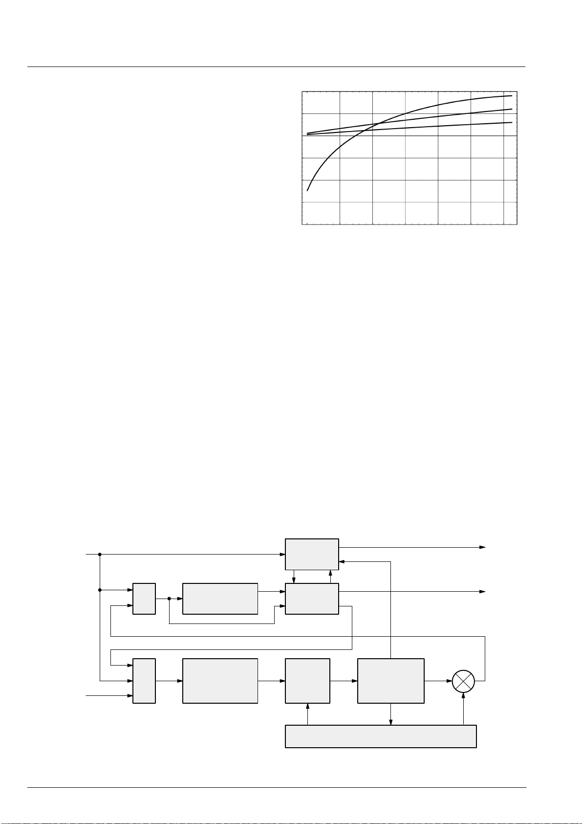
With off-air or mistuned reception, any attenuation at
higher frequencies or asymmetry around the color subcarrier is compensated. Four different settings of the IFcompensation are possible:
– flat (no compensation)
– 6 dB/octave
– 12 dB/octave
– 10 dB/MHz
dB
10
5
0
–5
10
15
20
3.5 3.75 4 4.25 4.5 5
4.75
MHz
Fig. 2–3: Freq. response of chroma IF-compensation
2.2.2. Demodulator
The entire signal (which might still contain luma) is now
quadrature-mixed to the baseband. The mixing frequency is equal to the subcarrier for PAL and NTSC, thus
achieving the chroma demodulation. For SECAM, the
mixing frequency is 4.286 MHz giving the quadrature
baseband components of the FM modulated chroma.
After the mixer, a lowpass filter selects the chroma components; a downsampling stage converts the color difference signals to a multiplexed half rate data stream.
The last setting gives a very large boost to high frequencies. It is provided for SECAM signals that are decoded
using a SAW filter specified originally for the PAL standard.
Luma / CVBS
MUXMUX
Chroma
1 H Delay
IF Compensation
DC-Reject
The subcarrier frequency in the demodulator is generated by direct digital synthesis; therefore, substandards
such as PAL 3.58 or NTSC 4.43 can also be demodulated.
Notch
Filter
CrossSwitch
MIXER
ACC
Lowpass Filter
Phase/Freq.
Demodulator
Luma
Chroma
Fig. 2–4: Color decoder
Color-PLL/Color-ACC
10 Micronas
Page 11

PRELIMINARY DATA SHEET
VPX 3225D, VPX 3224D
2.2.3. Chrominance Filter
The demodulation is followed by a lowpass filter for the
color difference signals for P AL/NTSC. SECAM requires
a modified lowpass function with bell-filter characteristic.
At the output of the lowpass filter, all luma information is
eliminated.
The lowpass filters are calculated in time multiplex for
the two color signals. Four bandwidth settings (narrow,
normal, broad, wide) are available for each standard.
The filter passband can be shaped with an extra peaking
term at 1.25 MHz. For P AL/NTSC, a wide band chroma
filter can be selected. This filter is intended for high
bandwidth chroma signals; for example, a nonstandard
wide bandwidth S-VHS signal.
dB
0
–10
–20
–30
–40
2.2.4. Frequency Demodulator
The frequency demodulator for demodulating the SECAM signal is implemented as a CORDIC-structure. It
calculates the phase and magnitude of the quadrature
components by coordinate rotation.
The phase output of the CORDIC processor is differentiated to obtain the demodulated frequency . After a programmable deemphasis filter, the Dr and Db signals are
scaled to standard C
amplitudes and fed to the cross-
rCb
over-switch.
2.2.5. Burst Detection
In the PAL/NTSC-system, the burst is the reference for
the color signal. The phase and magnitude outputs of
the CORDIC are gated with the color key and used for
controlling the phase-lock-loop (APC) of the demodulator and the automatic color control (ACC) in P AL/NTSC.
The ACC has a control range of +30...–6 dB.
For SECAM decoding, the frequency of the burst is measured. Thus, the current chroma carrier frequency can
be identified and is used to control the SECAM processing. The burst measurements also control the color killer operation; they can be used for automatic standard
detection as well.
–50
012345
PAL/NTSC
dB
0
–10
–20
–30
–40
–50
012345
SECAM
MHz
MHz
Fig. 2–5: Frequency response of chroma filters
2.2.6. Color Killer Operation
The color killer uses the burst-phase / burst-frequency
measurement to identify a PAL/NTSC or SECAM color
signal. For PAL/NTSC, the color is switched off (killed)
as long as the color subcarrier PLL is not locked. For SECAM, the killer is controlled by the toggle of the burst frequency. The burst amplitude measurement is used to
switch off the color if the burst amplitude is below a programmable threshold. Thus, color will be killed for very
noisy signals. The color amplitude killer has a programmable hysteresis.
2.2.7. PAL Compensation/1-H Comb Filter
The color decoder uses one fully integrated delay line.
Only active video is stored.
The delay line application depends on the color standard:
– NTSC: 1-H comb filter or color compensation
– PAL: color compensation
– SECAM: crossover-switch
11Micronas
Page 12
VPX 3225D, VPX 3224D
PRELIMINARY DATA SHEET
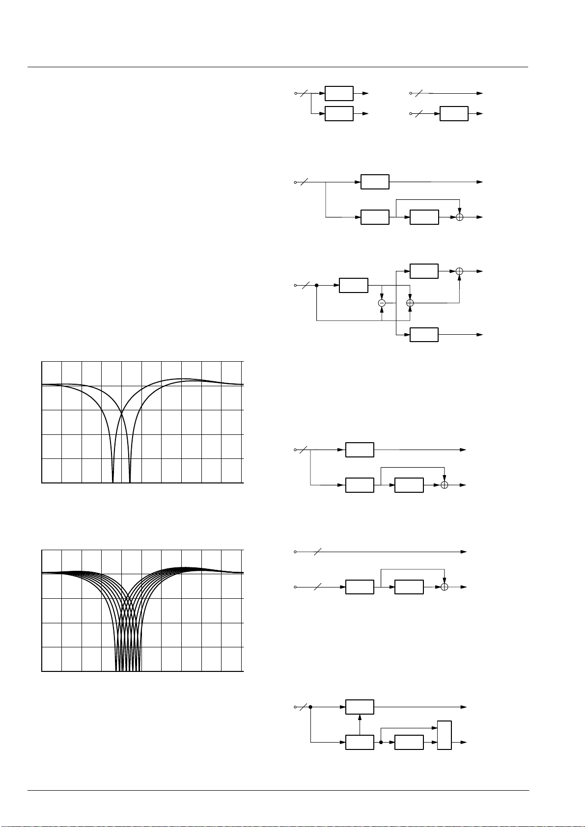
In the NTSC compensated mode, Fig. 2–7 c), the color
signal is averaged for two adjacent lines. Thus, crosscolor distortion and chroma noise is reduced. In the
NTSC combfilter mode, Fig. 2–7 d), the delay line is in
the composite signal path, thus allowing reduction of
cross-color components, as well as cross-luminance.
The loss of vertical resolution in the luminance channel
is compensated by adding the vertical detail signal with
removed color information.
2.2.8. Luminance Notch Filter
If a composite video signal is applied, the color information is suppressed by a programmable notch filter. The
position of the filter center frequency depends on the
subcarrier frequency for PAL/NTSC. For SECAM, the
notch is directly controlled by the chroma carrier frequency. This considerably reduces the cross-luminance. The frequency responses for all three systems
are shown in Fig. 2–6. In S-VHS mode, this filter is bypassed.
dB
10
CVBS
8
Notch
filter
Chroma
Process.
Y
C C
r b
Luma
8
Chroma
8
a) conventional b) S-VHS
CVBS
8
Notch
filter
Chroma
Process.
1 H
Delay
c) compensated
Notch
CVBS
8
1 H
Delay
filter
Chroma
Process.
d) comb filter
Chroma
Process.
Y
Y
CrC
Y
CrC
CrC
b
b
b
0
–10
–20
–30
–40
024 68 10
PAL/NTSC notch filter
dB
10
0
–10
–20
–30
MHz
Fig. 2–7: NTSC color decoding options
CVBS
8
Notch
filter
Chroma
Process.
1 H
Delay
a) conventional
Luma
8
Chroma
Chroma
8
Process.
1 H
Delay
b) S-VHS
Fig. 2–8: PAL color decoding options
Y
Y
CrC
CrC
b
b
–40
024 68 10
SECAM notch filter
Fig. 2–6: Frequency responses of the luma
notch filter for PAL, NTSC, SECAM
MHz
CVBS
8
Notch
filter
Chroma
Process.
1 H
Delay
MUX
Y
CrC
b
Fig. 2–9: SECAM color decoding
12 Micronas
Page 13

PRELIMINARY DATA SHEET
VPX 3225D, VPX 3224D
2.3. Video Sync Processing
Fig. 2–10 shows a block diagram of the front-end sync
processing. To extract the sync information from the
video signal, a linear phase lowpass filter eliminates all
noise and video contents above 1 MHz. The sync is separated by a slicer; the sync phase is measured. The internal controller can select variable windows to improve
the noise immunity of the slicer. The phase comparator
measures the falling edge of sync, as well as the integrated sync pulse.
The sync phase error is filtered by a phase-locked loop
that is computed by the FP. All timing in the front-end is
derived from a counter that is part of this PLL, and it thus
counts synchronously to the video signal.
A separate hardware block measures the signal back
porch and also allows gathering the maximum/minimum
of the video signal. This information is processed by the
FP and used for gain control and clamping.
For vertical sync separation, the sliced video signal is integrated. The FP uses the integrator value to derive vertical sync and field information.
2.4. Macrovision Detection (version D4 only)
Video signals from Macrovision encoded VCR tapes are
decoded without loss of picture quality . However, it might
be necessary in some applications to detect the presence of Macrovision encoded video signals. This is possible by reading a set of I2C registers (FP-RAM
0x170–0x179) in the video front-end.
Macrovision encoded video signals typically have AGC
pulses and pseudo sync pulses added during VBI. The
amplitude of the AGC pulses is modulated in time. The
Macrovision detection logic measures the VBI lines and
compares the signal against programmable thresholds.
The window in which the video lines are checked for Macrovision pulses can be defined in terms of start and stop
line (e.g. 6–15 for NTSC).
Frequency and phase characteristics of the analog video signal are derived from PLL1. The results are fed to
the rest of the video processing system in the backend.
The resizer unit uses them for data interpolation and
orthogonalization. A separate timing block derives the
timing reference signals HREF and VREF from the horizontal sync.
video
input
lowpass
1 MHz &
sync
slicer
horizontal
sync
separation
phase
comparator
& lowpass
counter
PLL1
front
sync
generator
front sync
skew
vblank
field
clamp &
signal
measurement
Fig. 2–10: Sync separation block diagram
clamping
front-end
timing
color key FIFO_write
clock
synthesizer
syncs
clock
H/V syncs
13Micronas
Page 14
VPX 3225D, VPX 3224D
PRELIMINARY DATA SHEET
2.5. Component Processing
Recovery of the YCbCr components by the decoder is
followed by horizontal resizing and skew compensation.
Contrast enhancement with noise shaping can also be
applied to the luminance signal. Vertical resizing is supported via line dropping.
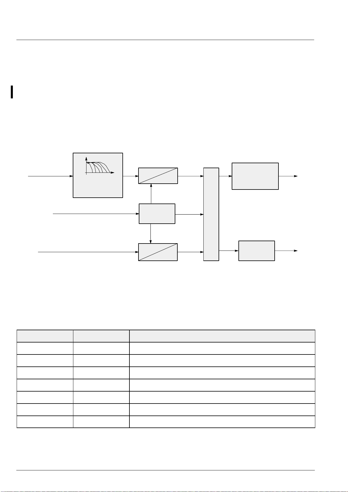
Fig. 2–11 illustrates the signal flow through the component processing stage. The YCbCr 4:2:2 samples are
separated into a luminance path and a chrominance
Y
in
Active Video
Reference
Luma Filter
with peaking
& coring
Resize
Sequence
Control
path. The Luma Filtering block applies anti-aliasing lowpass filters with cutoff frequencies adapted to the number of samples after scaling, as well as peaking and coring. The Resize and Skew blocks alter the effective
sampling rate and compensate for horizontal line skew.
The YCbCr samples are buffered in a FIFO for continuous burst at a fixed clock rate. For luminance samples,
the contrast and brightness can be adjusted and noise
shaping applied. In the chrominance path, Cb and Cr
samples can be swapped. Without swapping, the first
valid video sample is a Cb sample. Chrominance gain
can be adjusted in the color decoder.
Contrast,
Skew
Luma
Phase Shift
Latch
F
I
F
O
Brightness &
Noise shaping
Y
out
CbCr
Chroma
Phase Shift
in
Resize
Skew
16 bit
Cb/Cr-
swapping
Fig. 2–11: Component processing stage
Table 2–2: Several rasters supported by the resizer
NTSC PAL/SECAM Format Name
640 x 480 768 x 576 Square pixels for broadcast TV (4:3)
704 x 480 704 x 576 Input Raster for MPEG-2
320 x 240 384 x 288 Square pixels for TV (quarter resolution)
352 x 240 352 x 288 CIF – Input raster for MPEG-1, H.261
160 x 120 192 x 144 Square pixels for TV (1/16 resolution), H.324, H.323
Cr
out
176 x 120 176 x 144 QCIF – Input raster for H.261
32 x 24 32 x 24 Video icons for graphical interfaces (square)
14 Micronas
Page 15
VPX 3225D, VPX 3224DPRELIMINARY DATA SHEET
2.5.1. Horizontal Resizer
The operating range of the horizontal resizer was chosen to serve the widest possible range of applications
and source formats (number of lines, aspect ratio, etc...).
T able 2–2 lists several examples for video sourced from
525/625 line TV systems.
The horizontal resizer alters the sampling raster of the
video signal, thereby varying the number of pixels (NPix)
in the active portion of the video line. The number of pixels per line is selectable within a range from 32 to 864
in increments of 2 pixels (see section 2.10.: Windowing
the Video Field). T able 2–2 gives an overview of several
supported video rasters. The visual quality of a sampling
rate conversion operation depends on two factors:
– the frequency response of the individual filters, and
– the number of available filters from which to choose.
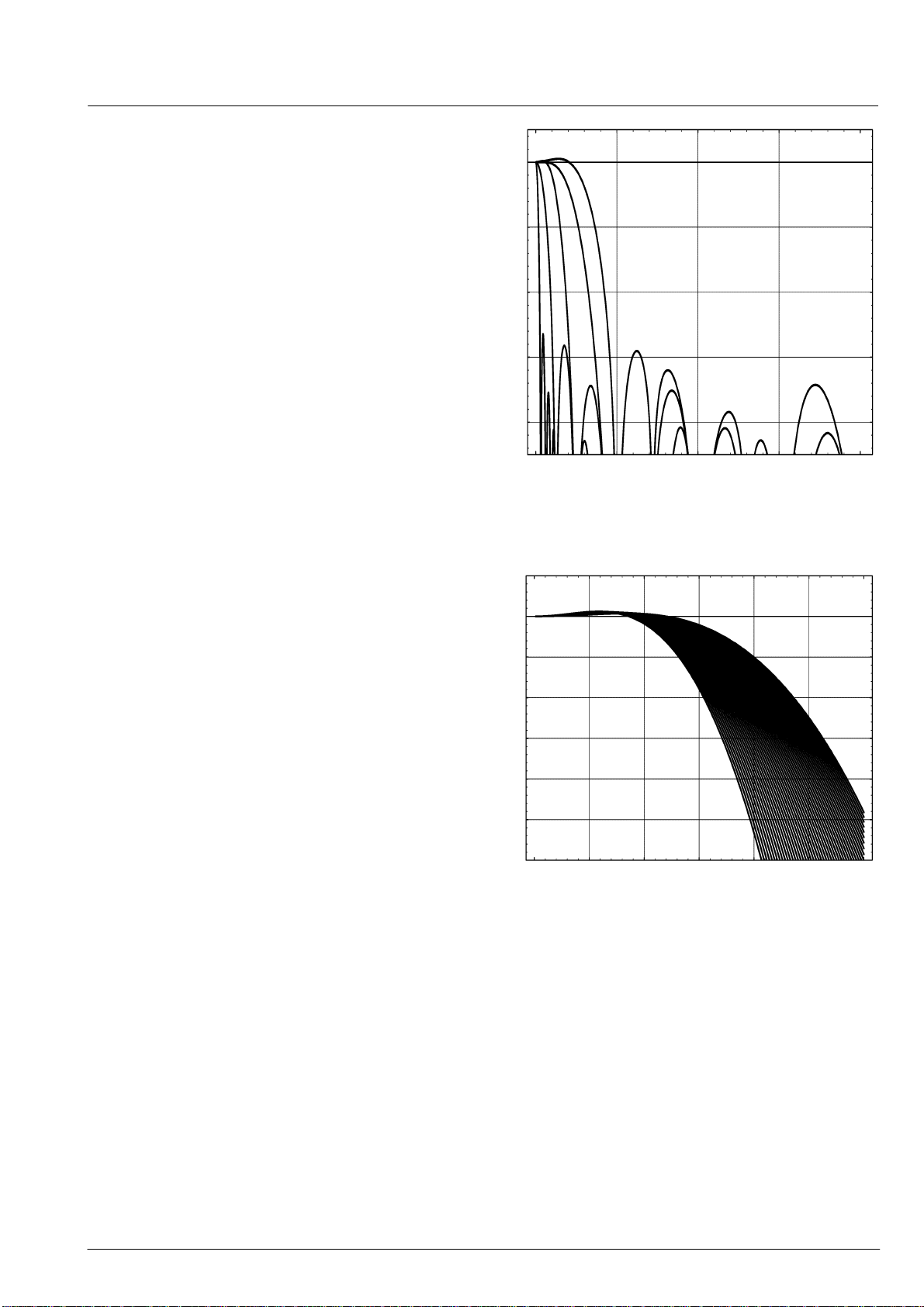
The VPX is equipped with a battery of FIR filters to cover
the five octave operating range of the resizer. Fig. 2–12
shows the magnitude response of five example filters
corresponding to 1054, 526, 262, 130, and 32 pixels.
The density of the filter array can be seen in Fig. 2–13.
The magnitude response of 50 filters lying next to each
other are shown. Nevertheless, these are only 10% of all
filters shown. As a whole, the VPX comes with a battery
of 512 FIR filters. Showing these 512 Filters in Fig. 2–12
would result in a large black area. This dense array of filters is necessary in order to maintain constant visual
quality over the range of allowable picture sizes. The alternative would be to use a small number of filters whose
cutoff frequencies are regularly spaced over the spectrum. However, it has been found that using few filters
leads to visually annoying threshold behavior. These effects occur when the filters are changed in response to
variations in the picture size.
dB
0
10
20
30
40
010203040
MHz
Fig. 2–12: Freq. response of 5 widely spaced filters
dB
0
–2
–4
–6
–8
10
Filter selection is performed automatically by the internal
processor based on the selected resizing factor (NPix).
This automated selection is optimized for best visual
performance.
12
0 0.5 1.5 2 3
1 2.5
Fig. 2–13: Freq. response of 50 neighbored filters
MHz
15Micronas
Page 16
VPX 3225D, VPX 3224D
PRELIMINARY DATA SHEET
2.5.2. Skew Correction
The VPX delivers orthogonal pixels with a fixed clock
even in the case of non-broadcast signals with substantial horizontal jitter (VCRs, laser disks, certain portions
of the 6 o’clock news...).
This is achieved by highly accurate sync slicing combined with post correction. Immediately after the analog
input is sampled, a horizontal sync slicer tracks the position of sync. This slicer evaluates, to within 1.6 ns, the
skew between the sync edge and the edge of the pixelclock. This value is passed as a skew on to the phase
shift filter in the resizer. The skew is then treated as a
fixed initial offset during the resizing operation.
The skew block in the resizer performs programmable
phase shifting with subpixel accuracy . In the luminance
path, a linear interpolation filter provides a phase shift
between 0 and 31/32 in steps of 1/32. This corresponds
to an accuracy of 1.6 ns. The chrominance signal can be
shifted between 0 and 7/8 in steps of 1/8.
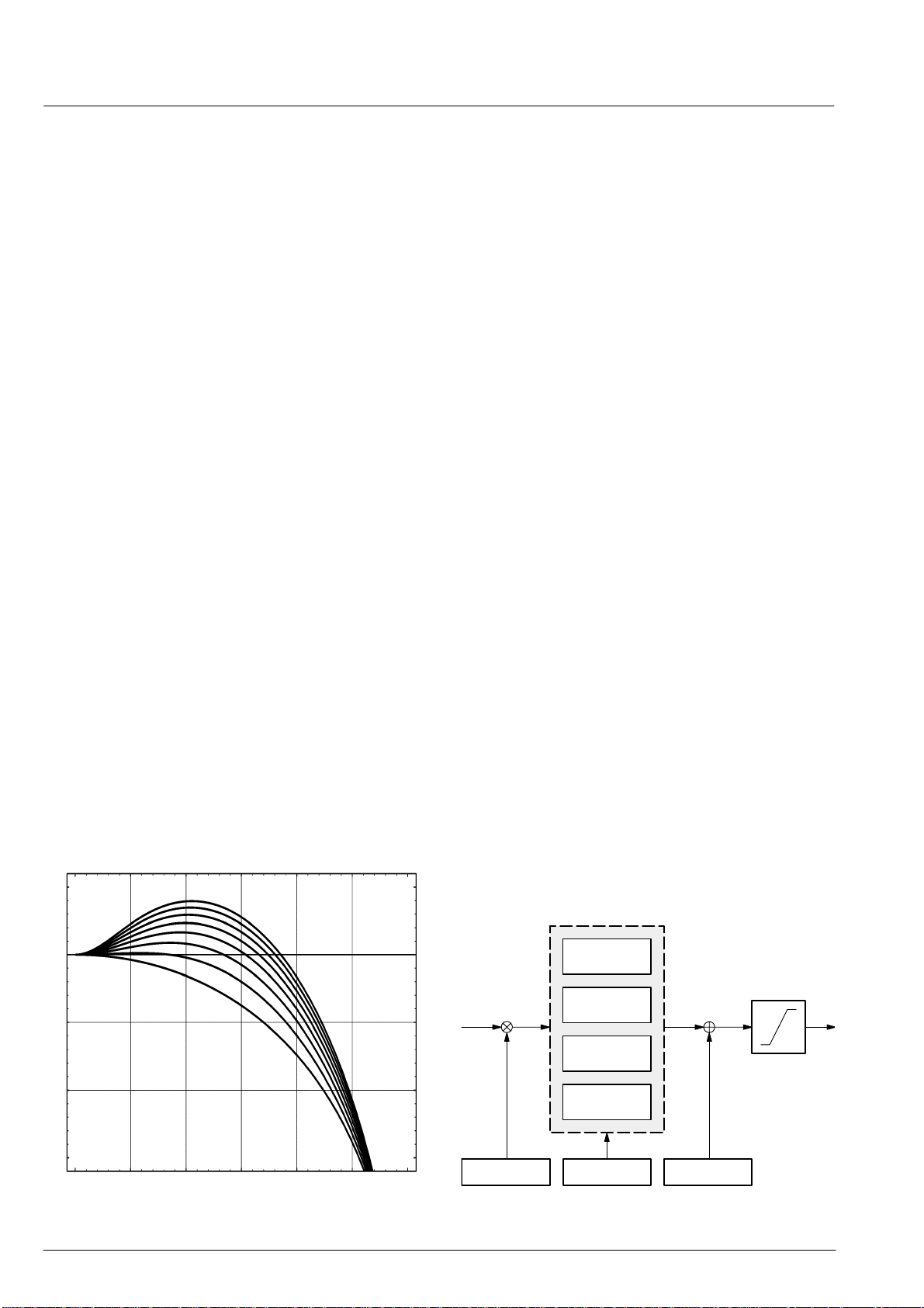
2.5.3. Peaking and Coring
The horizontal resizer comes with an extra peaking filter
for sharpness control. The center frequency of the peaking filter is automatically adjusted to the image size in
512 steps. The peaking value to each center frequency
can be controlled by the user with up to eight steps via
FP-RAM 0x126/130. Fig. 2–14 shows the magnitude response of the eight steps of the peaking filter corresponding to an image size of 320 pixels.
2.5.4. YCbCr Color Space
The color decoder outputs luminance and one multiplexed chrominance signal at a sample clock of
20.25 MHz. Active video samples are flagged by a separate reference signal. Internally, the number of active
samples is 1080 for all standards (525 lines and 625
lines). The representation of the chroma signals is the
ITU-R 601 digital studio standard.
In the color decoder, the weighting for both color difference signals is adjusted individually . The default format
has the following specification:
– Y = 224*Y + 16 (pure binary),
– C
= 224*(0.713*(R–Y)) + 128 (offset binary),
r
– C
= 224*(0.564*(B–Y)) + 128 (offset binary).
b
2.5.5. Video Adjustments
The VPX provides a selectable gain (contrast) and offset
(brightness) for the luminance samples, as well as additional noise shaping. Both the contrast and brightness
factors can be set externally via I
2
C serial control of FPRAM 0x127,128,131, and 132. Fig. 2–15 gives a functional description of this circuit. First, a gain is applied,
yielding a 10-bit luminance value. The conversion back
to 8-bit is done using one of four selectable techniques:
simple rounding, truncation,1-bit error diffusion, or 2-bit
error diffusion. Bit[8] in the ‘contrast’-register selects between the clamping levels 16 and 32.
After the peaking filter, an additional coring filter is implemented to the horizontal resizer. The coring filter subtracts 0, 1/2, 1, or 2 LSBs of the higher frequency part of
the signal. Note, that coring can be performed independently of the peaking value adjustment.
dB
10
0
–10
–20
–30
01 34 6
25
MHz
Fig. 2–14: Frequency response of peaking filter
I
= c * I
out
+ b c = 0...63/32 in 64 steps
in
b = –127...128 in 256 steps
In the chrominance path, Cb and Cr samples can be
swapped with bit[8] in FP-RAM 0x126 or 130. Adjustment of color saturation and gain is provided via FPRAM 0x30–33 (see section 2.2.5.).
Rounding
Truncation
1 bit
Err. Diff.
2 bit
Err. Diff.
Contrast Select Brightness
FP-RAM
Registers
Fig. 2–15: Contrast and brightness adjustment
16 Micronas
Page 17
VPX 3225D, VPX 3224DPRELIMINARY DATA SHEET
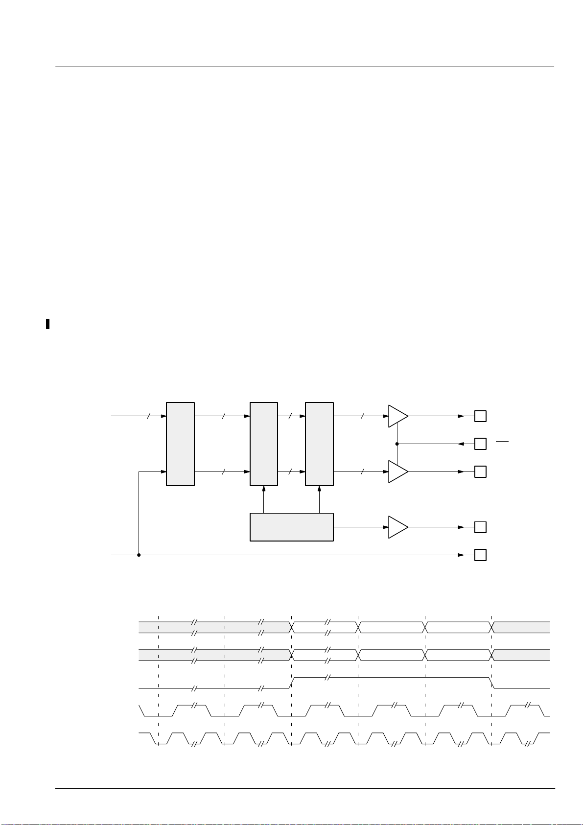
2.6. Video Output Interface
Contrary to the component processing stage running at
a clock rate of 20.25 MHz, the output formatting stage
(Fig. 2–16) receives the video samples at a pixel transport rate of 13.5 MHz. It supports 8 or 16-bit video formats with separate or embedded reference signals, provides bus shuffling, and channels the output via one or
both 8-bit ports. Data transfer is synchronous to the internally generated 13.5 MHz pixel clock.
The format of the output data depends on three parameters:
– the selected output format
S YUV 4:2:2, separate syncs
S YUV 4:2:2, ITU-R656
S YUV 4:2:2, embedded reference codes (BStream)
– the number of active ports (A only, or both A and B)
– clock speed (single, double, half).
In 8-bit modes using only Port A for video data, Port B
can be used as programmable output.
2.6.1. Output Formats
The VPX supports the YUV 4:2:2 video format only . During normal operation, all reference signals are output
separately. To provide a reduced video interface, the
VPX offers two possibilities for encoding timing references into the video data stream: an ITU-R656 compliant output format with embedded timing reference
headers and a second format with single timing control
codes in the video stream. The active output format can
be selected via FP-RAM 0x150 [format].
2.6.1.1. YUV 4:2:2 with Separate Syncs/ITU-R601
The default output format of the VPX is a synchronous
16-bit YUV 4:2:2 data stream with separate reference
signals. Port A is used for luminance and Port B for chrominance-information. Video data is compliant to ITUR601. Bit[1:0] of FP-RAM 0x150 has to be set to 00. Figure 2–17 shows the timing of the data ports and the
reference signals in this mode.
Video
Samples
Reference
Signals
16 8
Output Formats
Fig. 2–16: Output format stage
Luminance
(Port A)
Chrominance
(Port B)
VACT
8
8
Bus Shuffler
8
Clock
Generation
Output Multiplex
Y
1
C
1
8
8
Y
n–1
C
n–1
Y
n
C
n
Port A
OE
Port B
PIXCLK
LLC
LLC2
HREF
VREF
VACT
PIXCLK
LLC
Fig. 2–17: Detailed data output (single clock mode)
17Micronas
Page 18
VPX 3225D, VPX 3224D
PRELIMINARY DATA SHEET
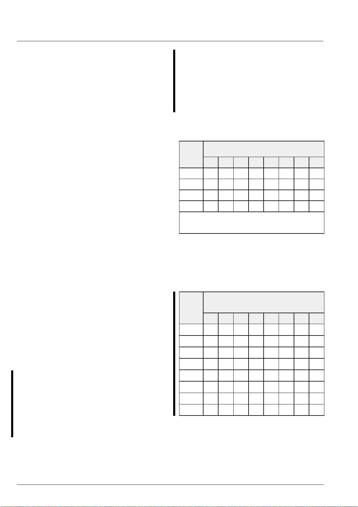
2.6.1.2. Embedded Reference Headers/ITU-R656
The VPX supports an output format which is designed to
be compliant with the ITU-R656 recommendation. It is
activated by setting Bit[1:0] of FP-RAM 0x150 to 01. The
16-bit video data must be multiplexed to 8 bit at the
double clock frequency (27 MHz) via FP-RAM 0x154, bit
9 set to 1 (see also section 2.6.3.: Output Multiplexer).
In this mode, video samples are in the following order:
Cb, Y, Cr, Y, ... The data words 0 and 255 are protected
since they are used for identification of reference headers. This is assured by limitation of the video data. Timing reference codes are inserted into the data stream at
the beginning and the end of each video line in the following way: A ‘Start of active video’-Header (SA V) is inserted before the first active video sample. The ‘end of
active video’-code (EA V) is inserted after the last active
video sample. They both contain information about the
field type and field blanking. The data words occurring
during the horizontal blanking interval between EA V and
SA V are filled with 0x10 for luminance and 0x80 for chrominance information. T able 2–3 shows the format of the
SAV and EAV header.
Note that the following changes and extensions to the
ITU-R656 standard have been included to support horizontal and vertical scaling, transmission of VBI-data,
etc.:
– Both the length and the number of active video lines
varies with the selected window parameters. For compliance with the ITU-R656 recommendation, a size of
720 samples per line must be selected for each window. To enable a constant line length even in the case
of different scaling values for the video windows, the
VPX provides a programmable ‘active video’ signal
(see section 2.8.4.).
– During blanked lines, the V ACT signal is suppressed.
VBI-lines can be marked as blanked or active, thus allowing the choice of enabled or suppressed V ACT during the VBI-window. The vertical field blanking flag (V)
in the SAV/EAV header is set to zero in any line with
enabled VACT signal (valid VBI or video lines).
– During blanked lines, SAV/EAV headers can be sup-
pressed in pairs with FP-RAM 0x150, bit9. To assure
vertical sync detection, some SAV/EAV headers are
inserted during field blanking.
– The flags F , V , and H encoded in the SAV/EA V headers
change on SAV. With FP-RAM 0x150, bit10 set to 1,
they change on EA V . The programmed windows, however, are delayed by one line. Header suppression is
applied for EAV/SAV pairs.
– For data within the VBI-window (e.g. sliced or raw tele-
text data), the user can select between limitation or reduction to 7-bit resolution with an additional LSB assuring odd parity (0 and 255 never occur). This option
can be selected via FP-RAM 0x150 [range].
– Ancillary data blocks may be longer than 255 bytes (for
raw data) and are transmitted without checksum. The
secondary data ID is used as high byte of the data
count (DC1; see Table 2–5).
– Ancillary data packets must not follow immediately af-
ter EAV or SAV.
– The total number of clock cycles per line, as well as
valid cycles between EAV and SAV may vary.
Table 2–3: Coding of the SAV/EAV-header
Bit No.
Word MSB LSB
7 6 5 4 3 2 1 0
First 1 1 1 1 1 1 1 1
Second 0 0 0 0 0 0 0 0
Third 0 0 0 0 0 0 0 0
Fourth 1 F V H P3 P2 P1 P0
F = 0 during field 1, F = 1 during field 2
V = 0 during active lines V = 1 during vertical field blanking
H = 0 in SAV, H = 1 in EAV
The bits P0, P1, P2, and P3 are protection bits. Their
states are dependent on the states of F, V, and H as
shown in Table 2–4.
Table 2–4: Coding of the protection bits
Bit No.
Code
(hex)
80 1 0 0 0 0 0 0 0
9D 1 0 0 1 1 1 0 1
AB 1 0 1 0 1 0 1 1
B6 1 0 1 1 0 1 1 0
C7 1 1 0 0 0 1 1 1
DA 1 1 0 1 1 0 1 0
EC 1 1 1 0 1 1 0 0
F1 1 1 1 1 0 0 0 1
MSB LSB
F V H P3 P2 P1 P0
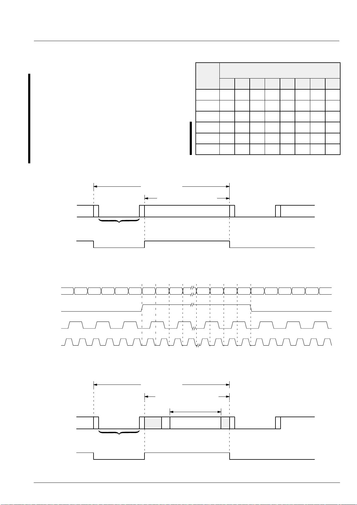
The VPX also supports the transmission of VBI-data as
vertical ancillary data during blanked lines in the interval
starting with the end of the SAV and terminating with the
beginning of EAV. In this case, an additional header is inserted directly before the valid active data. In this mode,
the position of SAV and EA V depends on the settings for
the programmable VACT signal. These parameters will
18 Micronas
Page 19
VPX 3225D, VPX 3224DPRELIMINARY DATA SHEET
be checked and corrected if necessary to assure an appropriate size of VACT for both data and ancillary header.
Table 2–5 shows the coding of the ancillary header information. The word I[2:0] contains a value for data type
identification (1 for sliced and 3 for raw data during odd
fields, 5 for sliced and 7 for raw data during even fields).
M[5:0] contains the MSBs and L[5:0] the LSBs of the
number of following D-words (32 for sliced data, 285 for
raw data). DC1 is normally used as secondary data ID.
The value 0 for M[5:0] in the case of sliced data marks
an undefined format. Bit 6 is even parity for bit5 to bit0.
Bit 7 is the inverted parity flag. Note that the following
user data words (video data) are either limited or have
odd parity to assure that 0 and 255 will not occur. Bit 3
in RAM 0x150 selects between these two options.
current line length
dependent on window size
Digital
Video Output
EAV
SAV
CB Y CR Y ...
Table 2–5: Coding of the ancillary header information
Bit No.
Word MSB LSB
7 6 5 4 3 2 1 0
Pream1 0 0 0 0 0 0 0 0
Pream2 1 1 1 1 1 1 1 1
Pream3 1 1 1 1 1 1 1 1
DID NP P 0 1 0 I2 I1 I0
DC1 NP P M5 M4 M3 M2 M1 M0
DC2 NP P L5 L4 L3 L2 L1 L0
CB Y CR Y ...
EAV
SAV
constant during
horizontal blanking
Y = 10
hex
; C
= C
= 80
R
B
hex
SAV: “start of active video” header
EAV: “end of active video” header
VACT
Fig. 2–18: Output of video or VBI data with embedded reference headers (according to ITU-R656)
DATA
(Port A)
VACT
PIXCLK
LLC
SAV1SAV2SAV3SAV
10h80h 80h 10hEAV1EAV2EAV3EAV
4
C
B1Y1
CR1Y2C
Bn–1Yn–1
C
Rn–1Yn
Fig. 2–19: Detailed data output (double clock mode)
current line length
size of programmable VACT
dependent on VBI-window size
4
Digital
Video Output
EAV
constant during
horizontal blanking
Y = 10
hex
; C
= C
R
B
= 80
SAV
hex
VACT
Fig. 2–20: Output of VBI-data as ancillary data
D1 D2 D3 D4 ...
ANC
CB Y CR Y ...
EAV
SAV: “start of active video” header
EAV: “end of active video” header
SAV
19Micronas
Page 20
VPX 3225D, VPX 3224D
PRELIMINARY DATA SHEET
2.6.1.3. Embedded Timing Codes (BStream)
In this mode, several event words are inserted into the
pixel stream for timing information. It is activated by setting Bit[1:0] of FP-RAM 0x150 to 10. Each event word
consists of a chrominance code value containing the
phase of the color-multiplex followed by a luminance
code value signalling a specific event. The allowed control codes are listed in table 2–6 and 2–7.
At the beginning and the end of each active video line,
timing reference codes (start of active video: SAV; end
of active video: EA V) are inserted with the beginning and
the end of VACT. Since VACT is suppressed during
blanked lines, video data and SA V/EA V codes are present during active lines only . If raw/sliced data should be
output, V ACT has to be enabled during the VBI window
with bit 2 of FP-RAM 0x138! In the case of several windows per field, the length of the active data stream per
line can vary. Since the qualifiers for active video (SAV/
EAV) are independent of the other reference codes,
there is no influence on horizontal or vertical syncs, and
sync generation can be performed even with several different windows. For full compliance with applications requiring data streams of a constant size, the VPX provides a mode with programmable ‘video active’ signal
V ACT which can be selected via bit 2 of FP-RAM 0x140.
The start and end positions of V ACT relative to HREF is
determined by FP-RAM 0x151 and 0x152. The delay of
valid data relative to the leading edge of HREF is calculated with the formulas given in table 2–8 and 2–9. The
result can be read in FP-RAM 0x10f (for window 1) and
0x1 1f (for window 2). Be aware that the largest window
defines the size of the needed memory. In the case of
1140 raw VBI-samples and only 32 scaled video samples, the graphics controller needs 570 words for each
line (the VBI-samples are multiplexed to luminance and
chrominance paths).
Table 2–6: Chrominance control codes
Chroma Value Phase Information
FE Cr pixel
FF Cb pixel
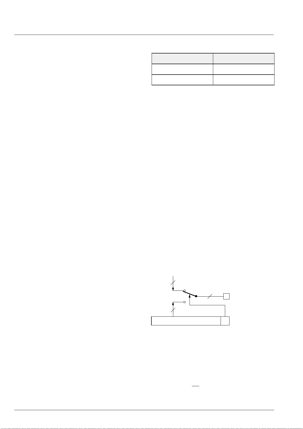
2.6.2. Bus Shuffler
In the YUV 4:2:2 mode, the output of luminance data is
on port A and chrominance data on Port B. With the bus
shuffler , luminance can be switched to Port B and chrominance to port A. In 8-bit double clock mode, shuffling
can be used to swap the Y and C components. It is selected with FP-RAM 0x150.
2.6.3. Output Multiplexer
During normal operation, a 16-bit YUV 4:2:2 data stream
is transferred synchronous to an internally generated
PIXCLK at a rate of 13.5 MHz. Data can be latched onto
the falling edge of PIXCLK or onto the rising edge of LLC
during high PIXCLK. In the double clock mode, luminance and chrominance data are multiplexed to 8 bit and
transferred at the double clock frequency of 27 MHz in
the order Cb, Y , Cr , Y ...; the first valid chrominance value
being a Cb sample. With shuffling switched on, Y and C
components are swapped. Data can be latched with the
rising edge of LLC or alternating edges of PIXCLK. This
mode is selected with bit 9 of FP-RAM 0x154. All 8-bit
modes use Port A only . In this case, Port B can be activated as programmable output with bit 8 of FP-RAM
0x154. Bit 0–7 determine the state of Port B.
video data
The leading edge of HREF indicates the beginning of a
new video line. Depending on the type of the current line
(active or blanked), the corresponding horizontal reference code is inserted. For big window sizes, the leading
edge of HREF can arrive before the end of the active
data. In this case, hardware assures that the control
8
=0
8
B[7:0]
video port
=1
8
code for HREF is delayed and inserted after EAV only.
The VREF control code is inserted at the falling edge of
7:0 8
VREF. The state of HREF at this moment indicates the
current field type (HREF = 0: odd field; HREF = 1: even
field).
FP-RAM 0x154 [outmux]
Fig. 2–21: Programmable output port
In this mode, the words 0,1,254, and 255 are reserved
for data identifications. This is assured by limitation of
the video data.
2.6.4. Output Ports
The two 8-bit ports produce TTL level signals coded in
binary offset. The Ports can be tristated either via the
output enable pin (OE
) or via I2C register 0xF2. For more
information, see section 2.17. “Enable/Disable of Output
Signals”.
20 Micronas
Page 21
VPX 3225D, VPX 3224DPRELIMINARY DATA SHEET
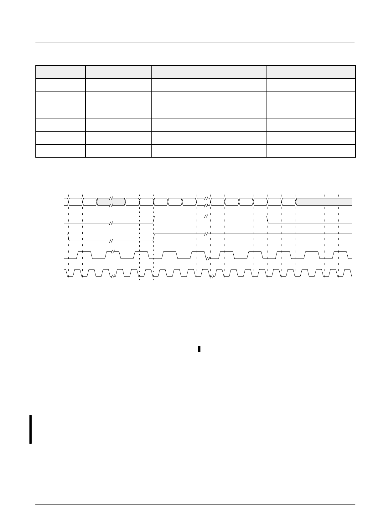
Table 2–7: Luminance control codes
Luma Value Video Event Video Event Phase Information
01 VACT end last pixel was the last active pixel refers to the last pixel
02 VACT begin next pixel is the first active pixel refers to the next pixel
03 HREF active line begin of an active video line refers to the current pixel
04 HREF blank line begin of a blank line refers to the current pixel
05 VREF even begin of an even field refers to the current pixel
06 VREF odd begin of an odd field refers to the current pixel
DATA
(Port A)
VACT
HREF
PIXCLK
LLC
FFh 02h03hFFh FEh 01h
C
B1Y1
CR1Y2C
Bn–1Yn–1
Fig. 2–22: Detailed data output with timing event codes (double clock mode)
2.7. Video Data Transfer
The VPX supports a synchronous video interface. Video
data arrives to each line at the output in an uninterrupted
burst with a fixed transport rate of 13.5 MHz. The duration of the burst is measured in clock periods of the transport clock and is equal to the number of pixels per output
line.
2.7.1. Single and Double Clock Mode
Data is transferred synchronous to the internally generated PIXCLK. The frequency of PIXCLK is 13.5 MHz.
The LLC signal is provided as an additional support for
both the 13.5 MHz and the 27 MHz double clock mode.
The LLC consists of a doubled PIXCLK signal (27 MHz)
for interface to external components which rely on the
Philips transfer protocols. In the single clock mode, data
The data transfer is controlled via the signals: PIXCLK,
V ACT, and LLC. An additional clock signal LLC2 can be
switched to the TDO output pin to support different timings.
can be latched onto the falling edge of PIXCLK or at the
rising edge of LLC during high PIXCLK. In double clock
mode, output data can be latched onto both clock edges
of PIXCLK or onto every rising edge of LLC. Combined
with the half-clock mode, the available transfer band-
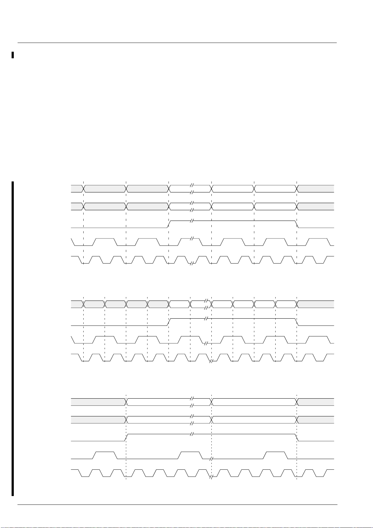
The V ACT signal flags the presence of valid output data.
Fig. 2–23, 2–24, and 2–25 illustrate the relationship be-
widths at the ports are therefore 6.75 MHz, 13.5 MHz,
and 27.0 MHz.
tween the video port data, VACT, PIXCLK, and LLC.
Whenever a line of video data should be suppressed
(line dropping, switching between analog inputs), it is
done by suppression of VACT.
C
Rn–1Yn
21Micronas
Page 22
VPX 3225D, VPX 3224D
2.7.2. Half Clock Mode
For applications demanding a low bandwidth for the
transmission between video decoder and graphics controller, the clock signal qualifying the output pixels
(PIXCLK) can be divided by 2. This mode is enabled by
setting Bit 5 of the FP-RAM 0x150 [halfclk]. Note that the
output format ITU-R601 must be selected. The timing of
the data and clock signals in this case is described in Figure 2–25.
If the half-clock mode is enabled, each second pulse of
PIXCLK is gated. PIXCLK can be used as a qualifier for
valid data. To ensure that the video data stream can be
spread, the selected number of valid output samples
should not exceed 400.
PRELIMINARY DATA SHEET
Luminance
(Port A)
Chrominance
(Port B)
VACT
PIXCLK
LLC
Fig. 2–23: Output timing in single clock mode
Video
(Port A)
VACT
PIXCLK
LLC
Y
1
C
1
C
Y
1
1
Y
n–1
C
n–1
C
n–1
Y
n–1
Y
n
C
n
C
Y
n
n
Fig. 2–24: Output timing in double clock mode
Luminance
(Port A)
Chrominance
(Port B)
VACT
PIXCLK
LLC
Y
1
C
1
Y
n
C
n
Fig. 2–25: Output timing in half clock mode
22 Micronas
Page 23
VPX 3225D, VPX 3224DPRELIMINARY DATA SHEET
2.8. Video Reference Signals
The complete video interface of the VPX runs at a clock
rate of 13.5 MHz. It mainly generates two reference signals for the video timing: a horizontal reference (HREF)
and a vertical reference (VREF). These two signals are
generated by programmable hardware and can be either free running or synchronous to the analog input video. The video line standard (625/50 or 525/60) depends
on the TV-standard selected with FP-RAM 0x20 [sdt].
The polarity of both signals is individually selectable via
FP-RAM 0x153.
The circuitry which produces the VREF and HREF signals has been designed to provide a stable, robust set
of timing signals, even in the case of erratic behavior at
the analog video input. Depending on the selected operating mode given in FP-RAM 0x140 [settm], the period
of the HREF and VREF signals are guaranteed to remain within a fixed range. These video reference signals
can therefore be used to synchronize the external components of a video subsystem (for example the ICs of a
PC add-in card).
In addition to the timing references, valid video samples
are marked with the ‘video active’ qualifier (V ACT). In order to reduce the signal number of the video interface,
several 8-bit modes have been implemented, where the
reference signals are multiplexed into the data stream
(see section 2.6.1.).
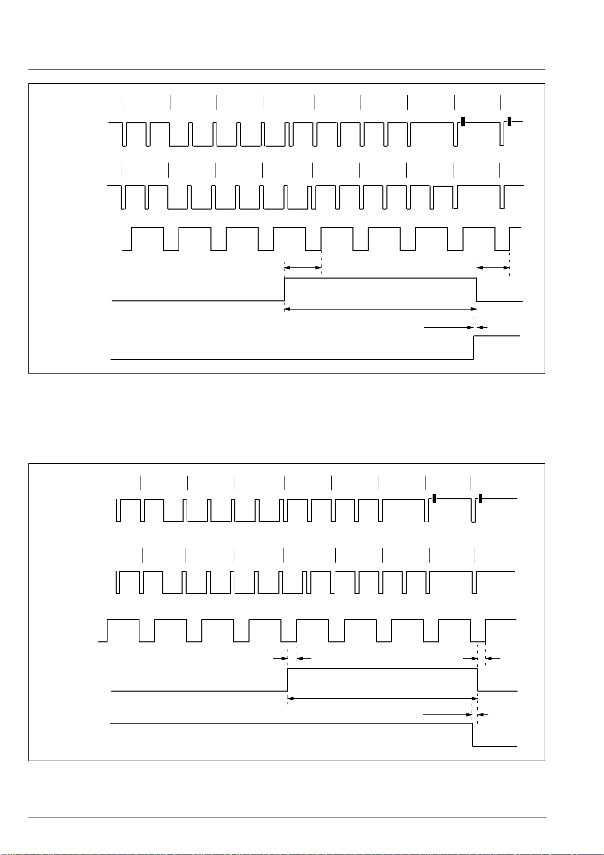
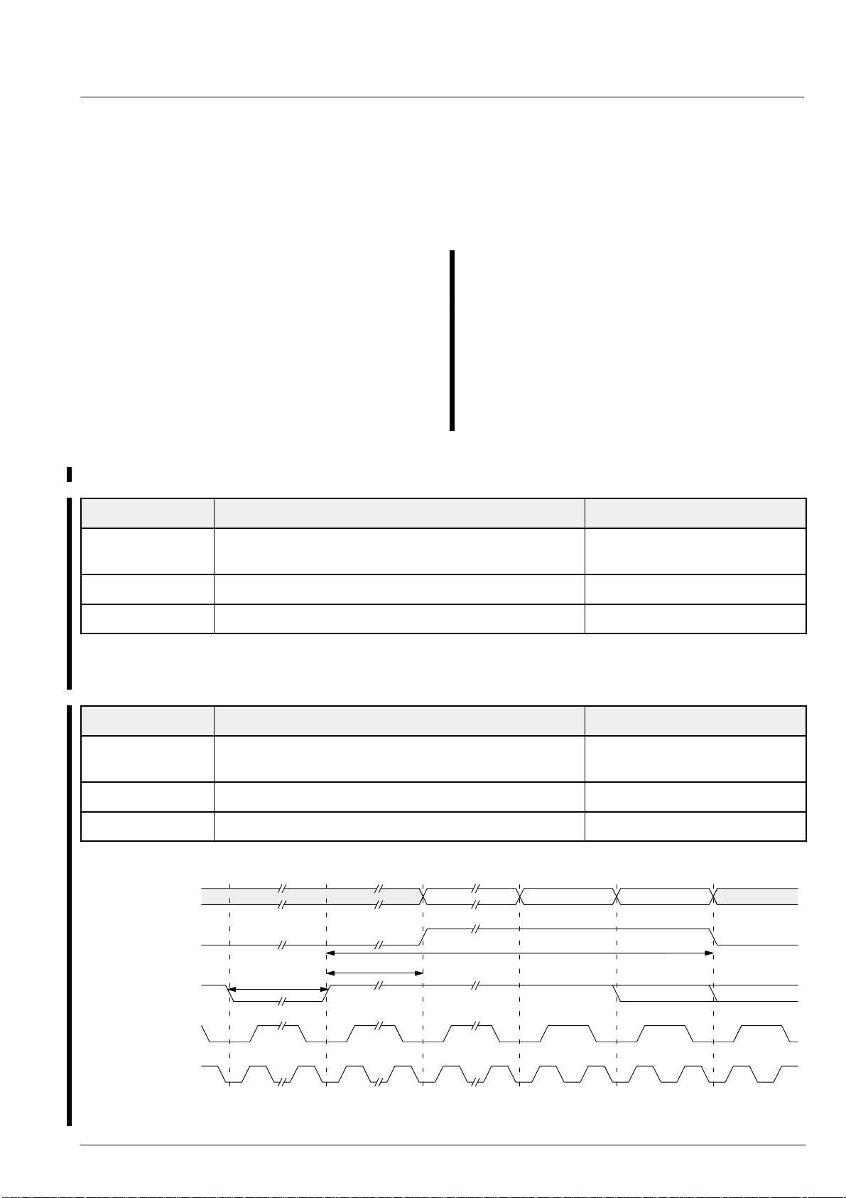
2.8.2. VREF
Figs. 2–27 and 2–28 illustrate the timing of the VREF
signal relative to field boundaries of the two TV standards. The start of the VREF pulse is fixed, while the
length is programmable in the range between 2 and 9
video lines via FP-RAM 0x153 [vlen].
2.8.3. Odd/Even Information (FIELD)
Information on whether the current field is odd or even
is supplied through the relationship between the edge
(either leading or trailing) of VREF and level of HREF.
This relationship is fixed and shown in Figs. 2–27 and
2–28. The same information can be supplied to the
FIELD pin, which can be enabled/disabled as output in
FP-RAM 0x153 [enfieldq]. FP-RAM 0x153 [oepol] programs the polarity of this signal.
During normal operation the FIELD flag is filtered since
most applications need interlaced signals. After filtering,
the field type is synchronized to the input signal only if
the last 8 fields have been alternating; otherwise, it always toggles. This filtering can be disabled with FPRAM 0x140 [disoef]. In this case, the field information
follows the odd/even property of the input video signal.
2.8.1. HREF
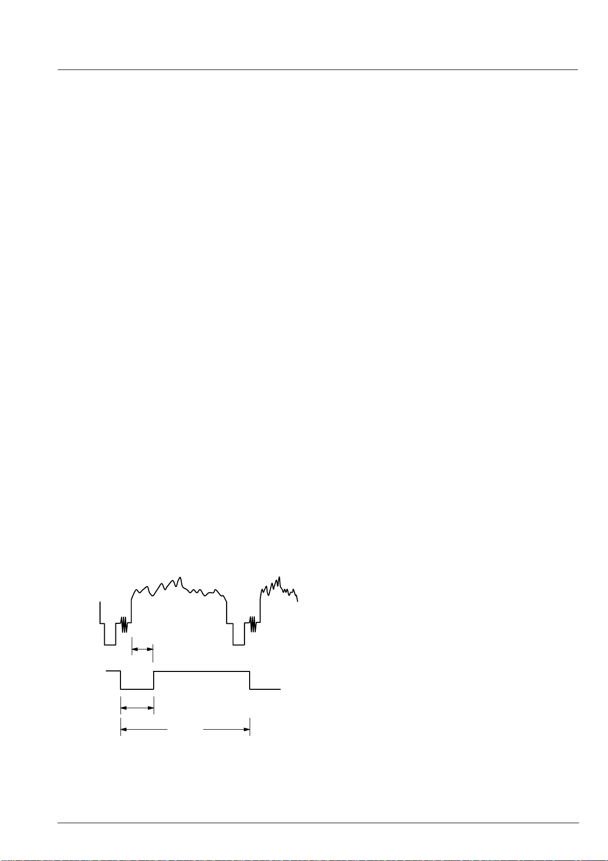
Fig. 2–26 illustrates the timing of the HREF signal relative to the analog input. The inactive period of HREF has
a fixed length of 64 periods of the 13.5 MHz output clock
rate. The total period of the HREF signal is expressed as
F
Analog
Video
Input
HREF
and depends on the video line standard.
nominal
VPX
Delay
4.7 µs (64 cycles)
F
nominal
Fig. 2–26: HREF relative to input video
23Micronas
Page 24
VPX 3225D, VPX 3224D
PRELIMINARY DATA SHEET
625
1234567
Input CVBS
(50 Hz), PAL
34567 8 910
Input CVBS
(60 Hz), NTSC
HREF
VREF
FIELD
Fig. 2–27: VREF timing for ODD fields
361 t
CLK13.5
2 .. 9 H
> 1 t
CLK13.5
361 t
CLK13.5
Input CVBS
(50 Hz), PAL
Input CVBS
(60 Hz), NTSC
HREF
VREF
FIELD
313 314 315 316 317 318 319312 320
265 266 267 268 269 270 271 272 273
46 t
CLK13.5
2 .. 9 H
46 t
> 1 t
CLK13.5
CLK13.5
Fig. 2–28: VREF timing for EVEN fields
24 Micronas
Page 25
VPX 3225D, VPX 3224DPRELIMINARY DATA SHEET
2.8.4. VACT
supported [FP-RAM 0x140, vactmode]. The start and
end position for the VACT signal relative to the trailing
The ‘video active’ signal is a qualifier for valid video samples. Since scaled video data is stored internally, there
are no invalid pixel within the V ACT interval. VACT has
edge of HREF can be programmed within a range of 0
to 864 [FP-RAM 0x151, 0x152]. In this case, VACT no
longer marks valid samples only.
a defined position relative to HREF depending on the
window settings (see section 2.10.). The maximal window length depends on the minimal line length of the input signal. It is recommended to choose window sizes of
less than 800 pixels. Sizes up to 864 are possible, but for
non-standard input lines, VACT is forced inactive 4
PIXCLK cycles before the next trailing edge of HREF.
The position of the valid data depends on the window
definitions. It is calculated from the internal processor.
The calculated delay of V ACT relative to the trailing edge
of HREF can be read via FP-RAM 0x10f (window 1) or
0x1 1f (window 2). T ables 2–8 and 2–9 show the formulas
for the position of valid data samples relative to the trail-
ing edge of HREF.
During the VBI-window, VACT can be enabled or suppressed with FP-RAM 0x138. Within this window, the
VPX can deliver either sliced text data with a constant
length of 64 samples or 1 140 raw input samples. For applications that request a uniform window size over the
whole field, a mode with a free programmable VACT is
Fig. 2–29 illustrates the temporal relationship between
the VACT and the HREF signals as a function of the
number of pixels per output line and the horizontal di-
mensions of the window. The duration of the inactive pe-
riod of the HREF is fixed to 64 clock cycles.
Table 2–8: Delay of valid output data relative to the trailing edge of HREF (single clock mode)
Mode Data Delay Data End
Video data (HBeg+HLen)*(720/NPix)–Hlen for NPix < 720
DataDelay + HLen
HBeg*(720/NPix) for NPix ≥ 720
Raw VBI data 150 720
Sliced VBI data 726 790
Table 2–9: Delay of valid output data relative to the trailing edge of HREF (half clock mode)
Mode Data Delay Data End
Video data (HBeg+HLen)*(720/NPix)–2*Hlen for NPix < 360
DataDelay + 2*HLen
HBeg*(720/NPix) for NPix ≥ 360
Raw VBI data not possible! not possible!
Sliced VBI data 662 790
DATA
(Port A or B)
VACT
data delay
64 cycles
HREF
D
1
D
n–1
D
n
data end
PIXCLK
LLC
Fig. 2–29: Relationship between HREF and VACT signals (single clock mode)
25Micronas
Page 26

VPX 3225D, VPX 3224D
PRELIMINARY DATA SHEET
2.9. Operational Modes
The relationship between the video timing signals
(HREF and VREF) and the analog input video is determined by the selected operational mode. Three such
modes are available: the Open Mode, the Forced
Mode, and the Scan Mode. These modes are selected
2
via I
C commands [FP-RAM 0x140, settm, lattm].
2.9.1. Open Mode
In the Open Mode, both the HREF and the VREF signal
track the analog video input. In the case of a change in
the line standard (i.e. switching between the video input
ports), HREF and VREF automatically synchronize to
the new input. When no video is present, both HREF and
VREF float to the idling frequency of their respective
PLLs. During changes in the video input (drop-out,
switching between inputs), the performance of the
HREF and VREF signals is not guaranteed.
2.9.2. Scan Mode
In the Scan Mode, the HREF and VREF signals are always generated by free running hardware. They are
therefore completely decoupled from the analog input.
The output video data is always suppressed.
The purpose of the Scan Mode is to allow the external
controller to freely switch between the analog inputs
while searching for the presence of a video signal. Information regarding the video (standard, source, etc...)
can be queried via I
2
C read.
In the Scan Mode, the video line standard of the VREF
and HREF signals can be changed via I
2
C command.
The transition always occurs at the first frame boundary
after the I
2
C command is received. Fig. 2–30, below,
demonstrates the behavior of the VREF signal during
the transition from the 525/60 system to the 625/50 system (the width of the vertical reference pulse is exaggerated for illustration).
I2C Command to
switch video timing standard
Selected timing standard
becomes active
time
VREF
f
odd
16.683 ms
f
even
33.367 ms 40.0 ms
f
odd
20.0 ms
f
even
f
odd
(525/60) (625/50)
Fig. 2–30: Transition between timing standards
26 Micronas
Page 27
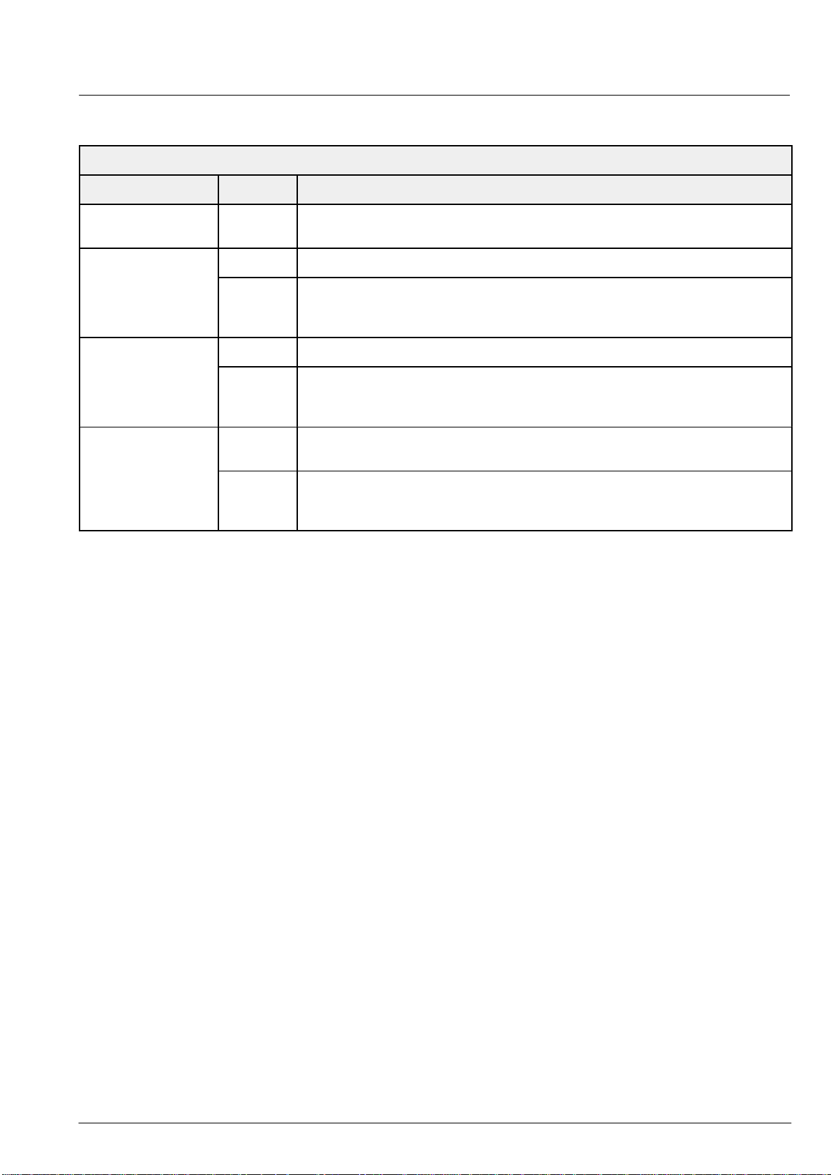
Table 2–10: Transition behavior as a function of operating mode
Transition Behavior as a Function of Operating Mode
Transition Mode Behavior
VPX 3225D, VPX 3224DPRELIMINARY DATA SHEET
Power up/Reset
(no video)
no video → video Open VREF, HREF: track the input signal
video → no video Open VREF, HREF: floats to steady state frequency of internal PLL
video → video Open VREF, HREF: track the input video immediately
Open VREF, HREF: floats to steady state frequency of internal PLL
Scan no visible effect on any data or control signals
– timing signals continue unchanged in free running mode
– VACT signal is suppressed
Scan no visible effect on any data or control signals
– timing signals continue unchanged in free running mode
– VACT signal is suppressed
Data: available immediately after color decoder locks to input.
Scan no outwardly visible effect on any data or control signals.
– timing signals continue unchanged in free running mode
– VACT signal is suppressed
27Micronas
Page 28
VPX 3225D, VPX 3224D
PRELIMINARY DATA SHEET
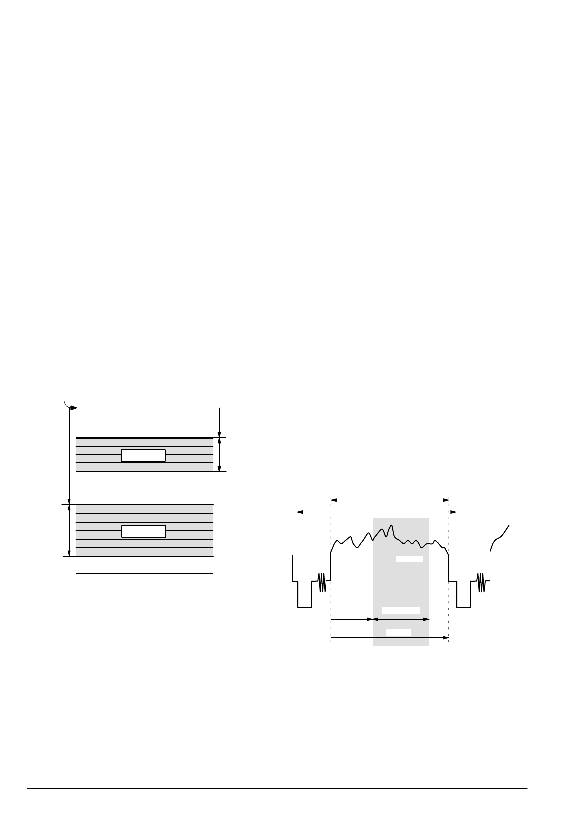
2.10. Windowing the Video Field
For each input video field, two non-overlapping video
windows can be defined. The dimensions of these windows are supplied via I
2
C commands. The presence of
two windows allows separate processing parameters
such as filter responses and the number of pixels per line
to be selected.
External control over the dimensions of the windows is
performed by I
2
C writes to a window-load-table (WinLoadT ab). For each window , a corresponding WinLoadT ab is defined in a table of registers in the FP-RAM [window1: 0x120–128; window2: 0x12a–132]. Data written
to these tables does not become active until the corresponding latch bit is set in the control register FP-
RAM 0x140. A 2-bit flag specifies the field polarity over
which the window is active [vlinei1,2].
Vertically, as can be seen in Fig. 2–31, each window is
defined by a beginning line given in FP-RAM 0x120/12A,
a number of lines to be read-in (FP-RAM 0x121/12B),
and a number of lines to be output (FP-RAM
0x122/12C). Each of these values is specified in units of
video lines.
Line 1
begin
begin
Window 1
# lines in,
# lines out
The option, to separately specify the number of input
lines and the number of output lines, enables vertical
compression. In the VPX, vertical compression is performed via simple line dropping. A nearest neighbor algorithm selects the subset of the lines for output. The
presence of a valid line is signalled by the ‘video active’
qualifier (or the corresponding SAV/EAV code in embedded sync modes).
The numbering of the lines in a field of interlace video is
dependent on the line standard. Figs. 2–33 and 2–34 illustrate the mapping of the window dimensions to the
actual video lines. The indices on the left are the line
numbers relative to the beginning of the frame. The indices on the right show the numbering used by the VPX.
As seen here, the vertical boundaries of windows are defined relative to the field boundary. Spatially, the lines
from field #1 are displayed above identically numbered
from field #2. For example: On an interlace monitor, line
#23 from field #1 is displayed directly above line #23
from field #2. There are a few restrictions to the vertical
definition of the windows. Windows must not overlap
vertically but can be adjacent. The first allowed line within a field is line #10 for 525/60 standards and line #7 for
625/50 standards. The number of output lines cannot be
greater than the number of input lines (no vertical zooming). The combined height of the two windows cannot
exceed the number of lines in the input field.
Horizontally , the windows are defined by a starting point
defined in FP-RAM 0x123/12D and the length in FPRAM 0x124/12E. They are both given relative to the
number of pixels (NPix) in the active portion of the line
(Fig. 2–32) selected in FP-RAM 0x125/12F . The scaling
factor is calculated internally from NPix.
# lines in,
# lines out
Window 2
Fig. 2–31: Vertical dimensions of windows
53.33 msec
64 msec
Window
H Begin H Length
N Pix
Fig. 2–32: Horizontal dimensions of sampling window
28 Micronas
Page 29

VPX 3225D, VPX 3224DPRELIMINARY DATA SHEET
4
5
6
7
18
19
20
21
260
261
262
263
264
265
260
261
262
263
264
265
266
260
261
262
263
264
265
266
4
267
5
268
6
269
7
270
18
19
20
21
281
282
283
284
523
524
525
1
2
3
D
D
D
D
D
D
4
5
6
7
18
19
20
21
D
D
D
D
D
D
Field 1 Field 2
Fig. 2–33: Mapping for 525/60 line systems
There are some restrictions in the horizontal window
definition. The total number of active pixels (NPix) must
be an even number. The maximum value for NPix should
be 800. V alues up to 864 are possible, but for short input
lines, video data is not guaranteed at the end of the line
since VACT will be interrupted at the beginning of the
next line. HLength should also be an even number. Obviously, the sum of HBegin and HLength may not be
greater than NPix.
Window boundaries are defined by writing the dimensions into the associated WinLoadTab and then setting
the corresponding latch bit in the control word FP-RAM
0x140 [latwin]. Window definition data is latched at the
beginning of the next video frame. Once the WinLoadTab data has been latched, the latch bit in the Control
word is reset. By polling the Infoword (FP-RAM 0x141),
the external controller can know when the window
boundary data has been read. Window definition data
can be changed only once per frame. Multiple window
definitions within a single frame time are ignored and
can lead to error.
308
309
310
311
312
313
308
309
310
311
312
313
1
2
3
4
22
23
24
25
314
315
316
317
335
336
337
338
621
622
623
624
625
D
D
D
D
D
D
1
2
3
4
22
23
24
25
D
D
D
D
D
D
1
2
3
4
22
23
24
25
308
309
310
311
312
Field 1 Field 2
Fig. 2–34: Mapping for 625/50 line systems
2.11. Temporal Decimation
T o cope with bandwidth restrictions in a system, the VPX
supports temporal dropping of video frames via suppression of the V ACT signal. Dropping will be applied for
video windows only. There is no influence on the state
of the VBI-window . This mode can be activated for each
video window by setting the enable flag in the corresponding WinLoadTab (FP-RAM 0x121/12B). The
selection in FP-RAM 0x157 determines how many
frames will be output within an interval of 3000 frames.
Note that this selection is applied for both video windows, but decimation can be enabled for each window
separately . The number of valid frames is updated only
if the corresponding latch flag in FP-RAM 0x140 [lattdec]
is set. Frame dropping with temporal decimation can be
combined with the field disable flags (FP-RAM
0x121/12B). Within valid video frames, each field type
can be disabled separately.
29Micronas
Page 30
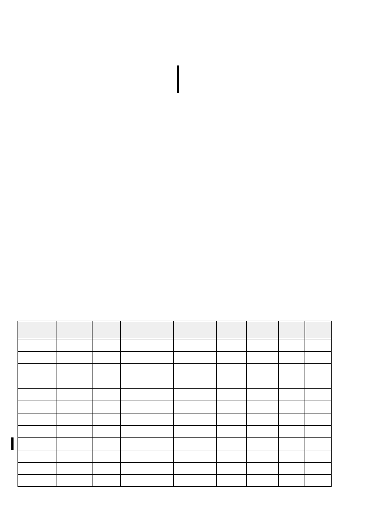
VPX 3225D, VPX 3224D
PRELIMINARY DATA SHEET
2.12. Data Slicer
The data slicer is only available on VPX 3225D. Software drivers accessing the slicer I
2
C registers should
therefore check the VPX part number.
2.12.1. Slicer Features
– 8-bit digital FBAS input
– 8-bit unbuffered ascii data output
– internal sync separation
– PAL and NTSC operation
– VBI and full-field mode
– automatic slicer adaptation
– text reception down to 30% eyeheight
– soft error correction
– simultaneous decoding of 4 different text services
• main service: programmable
• side service: VPS in line 16
• side service: CAPTION in line 21
• side service: WSS in line 23
2.12.2. Data Broadcast Systems
Table 2–11 gives an overview of the most popular data
broadcast systems throughout the world. The data slicer
of the VPX 3225D can be programmed to acquire the different data systems via a set of I2C registers.
The various data broadcast systems are specified by a
limited set of parameters:
– line multiplex (VBI)
– bit rate
– modulation
– start timing
– clock run-in (CRI)
– framing code (FRC)
– number of data bytes
– programmable text parameters for main service
• bit rate
• clock run-in
• framing code
• error tolerance
• number of data bytes
– operation controlled by I
2
C registers
Table 2–11: Data Broadcast Systems
Text
System
WST PAL 6–22 6.937500Mbit/s NRZ 10.3 µs ’5555’x ’27’x 42
VPS PAL 16 2.500000Mbit/s Bi-Phase 12.5 µs ’5555’x ’51’x 13
WSS PAL 23 0.833333Mbit/s Bi-Phase 11.0 µs ’3c78’x ’f8’x 11
Caption PAL 21 1.006993Mbit/s NRZ 10.5 µs ’aaa0’x ’c2’x 4
VITC PAL 6–22 1.812500Mbit/s NRZ 11.2 µs ? ? 9
Antiope SECAM 6–22 6.203125Mbit/s NRZ 10.5 µs ’5555’x ’e7’x 37
TV
StandardTVLines
Bitrate Modulation Timing CRI FRC No.
Bytes
WST NTSC 10–21 5.727272Mbit/s NRZ 9.6 µs ’5555’x ’27’x 34
NABTS NTSC 10–21 5.727272Mbit/s NRZ 10.5 µs ’5555’x ’e7’x 33
Caption NTSC 21 1.006993Mbit/s NRZ 10.5 µs ’aaa0’x ’c2’x 4
2xCaption NTSC 10–21 1.006993Mbit/s NRZ 10.5 µs ’2aa0’x ’b7’x 4
VITC NTSC 10–21 1.812500Mbit/s NRZ 11.2 µs ? ? 9
CGMS NTSC 20 0.450450Mbit/s NRZ 11 µs ’10’b – 3
30 Micronas
Page 31
VPX 3225D, VPX 3224DPRELIMINARY DATA SHEET
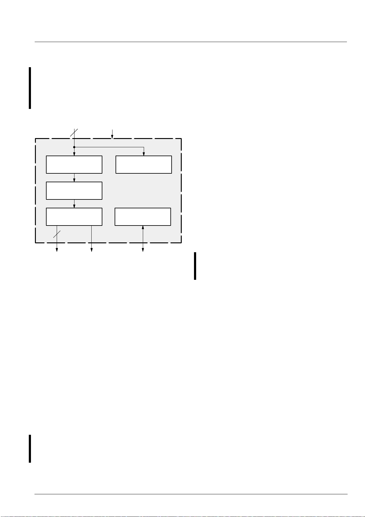
2.12.3. Slicer Functions
The data slicer is inserted between the video ADC and
the video output interface (see Fig. 1–1). It operates
completely independent of the video front-end processing and has its own sync separator and a separate set
of I2C registers. Figure 2–35 shows a more detailed
block diagram of the digital data slicer.
DIN
8
Bit Slicer
Formatter
20.25 MHz
SyncFilter
Digital
Text
Slicer
I2C Register
during framing code and clock run-in. The increment of
the phase accumulator is programmable and can be
used to set up any bit rate with the formula:
increment = 2048 * bit rate/20.25 MHz
2.12.3.3. Standard Selection
The main teletext service can be received in VBI lines
only or in every line of each field (full-field mode). All
parameters needed to identify a teletext service are
programmable.
The slicer uses a reference of 24 bits to identify a teletext
service. This reference is compared with the first
received teletext bits which are often named clock run-in
(CRI) and framing code (FRC). If there is a match, the
slicer will start signal adaptation and write the following
data to the output stage. The reference can be reduced
in length by setting a mask for services which do not
have a 16-bit clock run-in. Bit errors can be allowed by
setting a tolerance level for every byte of the reference.
8
2
Dout Dval
Fig. 2–35: Slicer block diagram
2.12.3.1. Input
The slicer receives an 8-bit digitized FBAS signal which
is clamped to the back porch level. The teletext signal
amplitude can vary to a certain degree (±3 dB), as the
slicer will adapt its internal slice level.
2.12.3.2. Automatic Adaptation
The slicer measures certain signal characteristics as DC
offset, level, bandwith, and phase error . A digital filter at
the input stage is used to compensate bandwith effects
of the transmission channel. A DC shifter generates a
DC free text signal even in case of co-channel interference. The internal slice level is adapted to the teletext
signal level.
The adaption algorithm is designed for the signal characteristics of a WST or NABTS transmission. For text
systems with significantly different signal characteristics
(like CAPTION), the adaption should be disabled.
The teletext sampling rate is generated by a phase accumulator running at 20.25 MHz, which is synchronized
C Bus
I
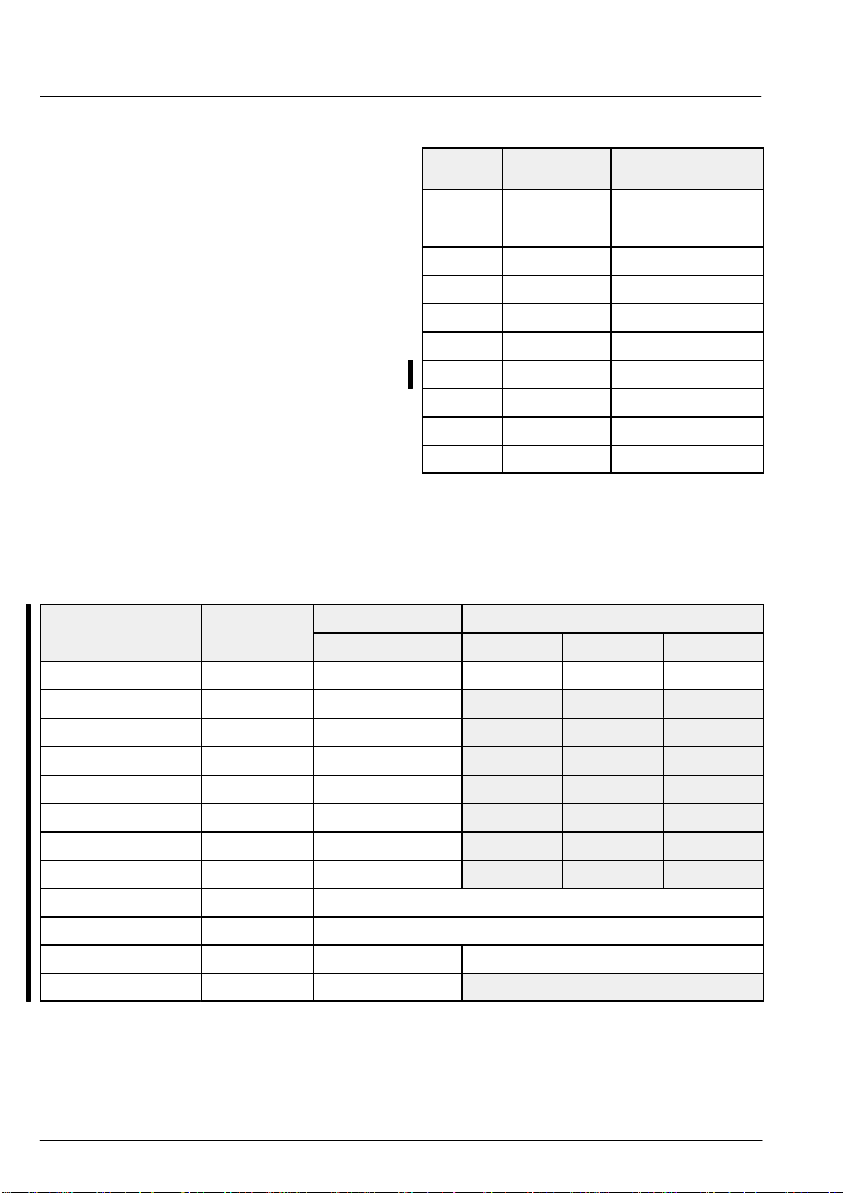
Additionally, the slicer can switch to other teletext
services during dedicated lines of the VBI. These can be
line 16 for VPS, line 21 for CAPTION, or line 23 for WSS.
In this case, the parameters are hard wired. Table 2–13
shows with which I2C registers the text parameters are
programmed and what the fixed settings for the side services are.
2.12.3.4. Output
The slicer delivers a synchronous burst of decoded
teletext data bytes together with a data valid signal. This
data stream is fed into the video FIFO of the VPX backend. The data rate depends on the teletext bit rate
(divided by 8), the length of the burst is programmable.
The burst can optionally be extended to 64 bytes independently of the selected teletext service (fill64 mode).
The dummy bytes needed to fill the burst to 64 bytes are
delivered at a rate of 20.25 MHz. Normally, there is no
output during lines without text transmission or unknown
text signals. For some applications, it is necessary to
have constant memory mapping. Therefore, the slicer
can be forced to output 64 bytes per line even if no text
is detected (dump mode).
The first 3 bytes of the data burst carry information to
identify the received teletext service. The 2 byte line
number contains a free running frame counter which can
be used to identify data loss in the framebuffer of a capture application. The field bit can be used to identify field
dependent services such as CAPTION. The 10-bit line
number corresponds to the standard line counting
scheme of a PAL composite video signal; in case of
NTSC, the value “3” is subtracted.
31Micronas
Page 32
VPX 3225D, VPX 3224D
Parameter
(hex)
PRELIMINARY DATA SHEET
The number of useful data bytes at the output is programmable and should be set accordingly to the selected teletext standard. T o get “n” data bytes, the value
“n+1” has to be programmed, because of the additional
framing code byte.
In case of dump mode, byte numbers “1” and “2” are also
valid for lines without detected text data. They are then
followed by 62 dummy bytes.
Table 2–12: Slicer Output Format
Byte
Number
1 line number
2 line number low b[7:0] line number[7:0]
3 framing code b[7:0] as transmitted
4 1st data byte b[7:0] as transmitted
. ... ...
byte_cnt+2 last data byte b[7:0] as transmitted
. dummy byte b[7:0] 00000000
. ... ...
64 dummy byte b[7:0] 00000000
Byte
Format
high
Bit
Format
b[7:3] frame counter
b[2] odd field
b[1:0] line number[9:8]
Table 2–13: Slicer Programming (shaded values are hard wired)
Programmable
text reception C9 on/off on/off on/off on/off
TV standard C9 pal/ntsc pal pal ntsc
TV lines C9 vbi/full field 16 23 21
bitrate C1, C2 702 506 506 102
reference BB, BC, BD 27 55 55 51 55 55 f8 3c 78 c2 aa a0
mask B8, B9, BA 00 00 03 00 00 00 00 00 00 00 00 1f
tolerance CE 01 01 01 01 01 01 01 01 01 01 01 01
byte_cnt CF 43 28 14 5
64 byte mode CF on/off
dump mode CF on/off
adaption C7 on/off off
soft error correction C7 on/off off
I2C Register
Main Service Side Services
e.g. WST VPS WSS CAPTION
32 Micronas
Page 33
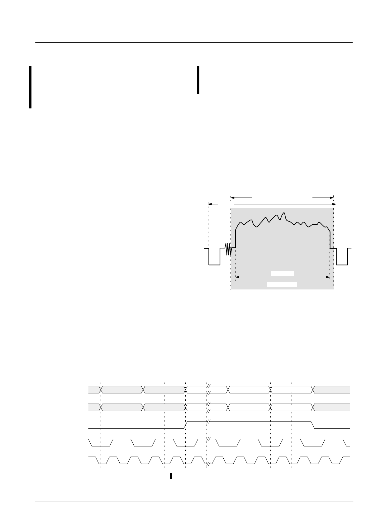
VPX 3225D, VPX 3224DPRELIMINARY DATA SHEET
2.13. VBI Data Acquisition
The VPX supports two different data acquisition modes
for the vertical blanking interval: a bypass mode for raw
data of the vertical blanking interval and a data slicer
mode in which dedicated hardware provides constant
packets of already decoded VBI-data. The data slicer
mode is only available on VPX 3225D.
For both services, the start and end line of a vertical
blanking interval (VBI) window can be defined for each
field with FP-RAM 0x134–137. Teletext data can occur
between lines 6 and 23 of each field. However, the VBIwindow is freely programmable. It is possible to select
the whole field (beginning with line #3). If video windows
are enabled, the VBI-window should end two lines before the first valid line of the next video window. The VBIwindow can be activated via bit[0] in FP-RAM 0x138.
The identification of valid VBI-lines is possible with the
V ACT-signal (or the ‘active line’-flags in the modes with
embedded syncs) or a special ‘data active’ signal on the
TDO pin. Bit[10] of FP-RAM 0x154 selects between
these two cases. In the default mode, V ACT is used. The
output of both signals can be suppressed optionally with
bit[2] of FP-RAM 0x138. In this case, the graphic controller has to use only the HREF signal to mask the active
video data.
2.13.1. Raw VBI Data
The raw data mode is enabled with bit[1] of FP-RAM
0x138 (vbimode). This mode bypasses the luminance
processing of the video front-end and delivers unmodified video samples from the ADC to the output ports.
During lines within the VBI-window, specified by the
user settings in the corresponding Load-T able, the VPX
internally acquires 1 140 raw data bytes of the luminance
input at a rate of 20.25 MHz corresponding to 56.296 µs
of the analog video (see Fig. 2–37). Chrominance data
is not valid. The raw data samples are multiplexed internally to 570x16 bit on the luminance and chrominance
port. The external timing corresponds to the video mode
with 570 output samples for an uncropped window.
Figure 2–36 shows the timing of both data ports and the
necessary reference signals in this mode.
1140 samples (56.296 ms)
64 ms
In the ITU-R656 mode, VBI-data can be transmitted as
vertical ancillary data (with 7 bit resolution + odd parity).
The selections for the VBI-window will be updated by
setting bit[11] in FP-RAM 0x138.
Luminance
(Port A)
Chrominance
(Port B)
VACT or TDO*
53.33 ms
active video
Fig. 2–37: Horizontal dimensions of the window
for raw VBI-data
D
2
D
1
D
D
1138
1137
D
D
1140
1139
PIXCLK
LLC
* depending on bit[10] of FP-RAM 0x154
Fig. 2–36: Timing during lines with raw VBI-data (single clock mode)
33Micronas
Page 34
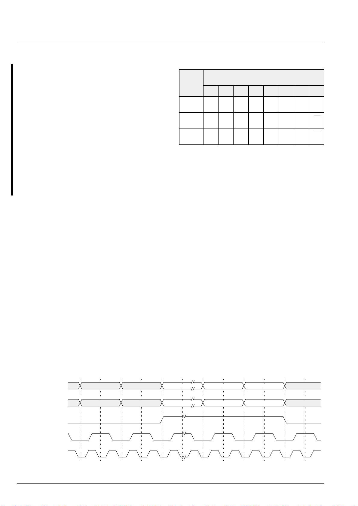
VPX 3225D, VPX 3224D
PRELIMINARY DATA SHEET
2.13.2. Sliced VBI Data
The sliced data mode is enabled with bit[1] of the
FP-RAM 0x138 (vbimode). This mode uses the integrated data slicer (available only on VPX 3225D) and
delivers decoded data samples to the output ports.
The data slicer provides data packets of a constant size
(filled with dummy bytes). The data packets have a default size of 64 bytes. T o reduce the data rate for text systems with a smaller number of data bytes, the packet
size can be reduced via FP-RAM 0x139.
During lines within the VBI-window, specified by the user
settings in the corresponding Load-T able, the VPX internally multiplexes the data slicer packets onto the luminance and chrominance outputs. Since the values 0,
254, and 255 are protected in the 8-bit output modes
(ITU-R656, BStream), each slicer sample is separated
into two nibbles for transmission. Table 2–14 shows the
implemented data formats.
In each path, one nibble is transmitted twice. The LSB
is inverted for odd parity . This assures that the values 0
and 255 will not occur (for the detection of embedded
syncs). In the mode with embedded timing event codes,
chrominance data will be limited additionally . No significant information will be lost since only Bit 0 and 1 will be
modified. Figure 2–38 shows the timing of data and reference signals in this mode.
Table 2–14: Splitting of sliced data to luminance and
chrominance output
Bit No.
Word MSB LSB
7 6 5 4 3 2 1 0
Slicer
Data
Chroma
Output
Luma
Output
S7 S6 S5 S4 S3 S2 S1 S0
S7 S6 S5 S4 S7 S6 S5 S4
S3 S2 S1 S0 S3 S2 S1 S0
The splitting described above can be disabled by setting
bit 6 in the ‘format_select’ register. In this case, the sliced
samples will be transmitted in the luminance path only.
T o avoid modification of valid data, the limitation of luminance data in the 8-bit output modes should be suppressed with bit 8 in the same register (note that luminance codes will not be protected).
Luminance
(Port A)
Chrominance
(Port B)
VACT
PIXCLK
LLC
D
1 (LSBs)
D
1 (MSBs)
D
63 (LSBs)
D
63 (MSBs)
D
64 (LSBs)
D
64 (MSBs)
Fig. 2–38: Timing during lines with sliced VBI-data (single clock mode)
34 Micronas
Page 35
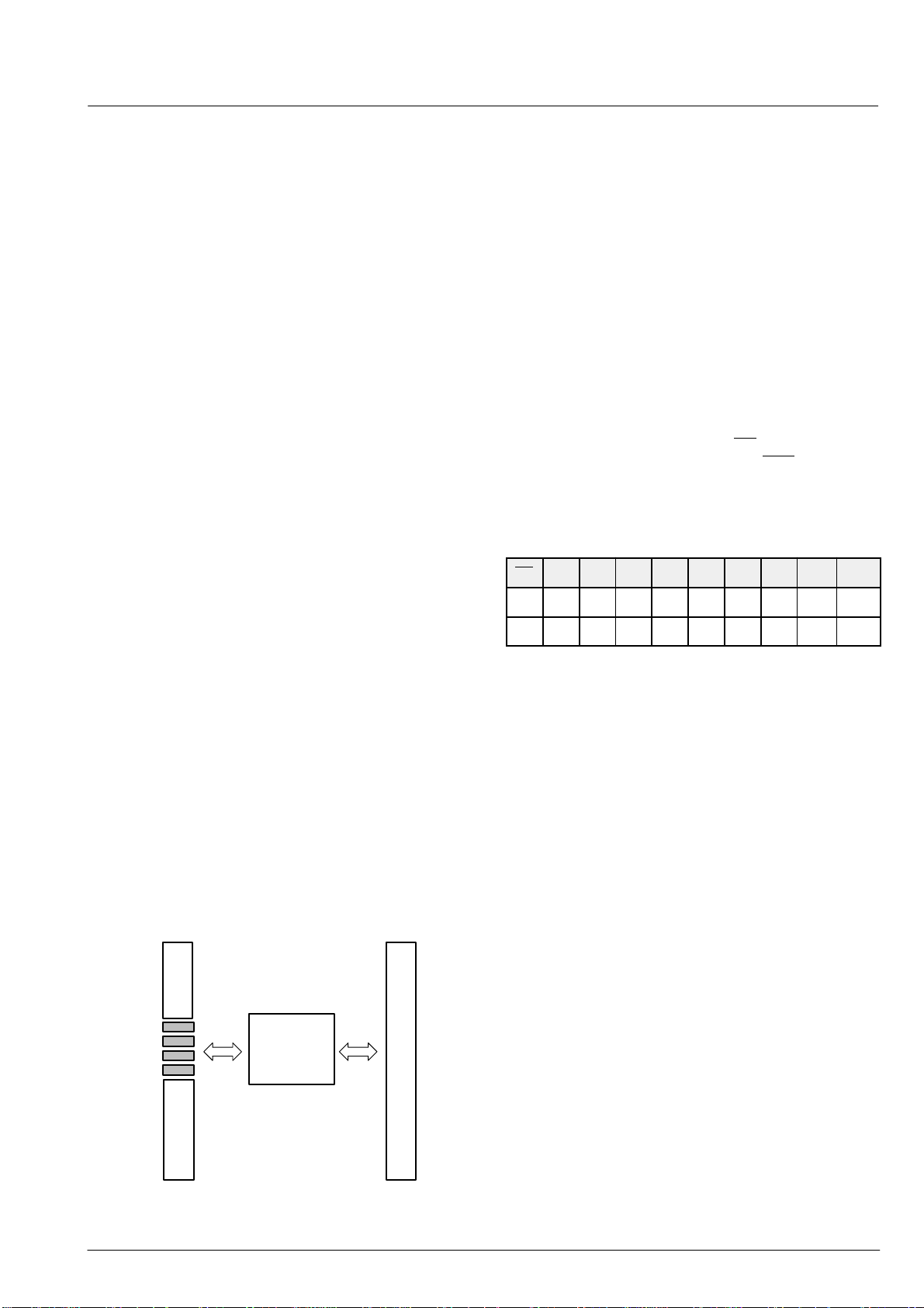
VPX 3225D, VPX 3224DPRELIMINARY DATA SHEET
2.14. Control Interface
2.14.1. Overview
Communication between the VPX and the external controller is performed serially via the I
2
C bus (pins SCL and
SDA).
There are basically two classes of registers in the VPX.
The first class of registers are the directly addressable
2
I
C registers. These are registers embedded directly in
the hardware. Data written to these registers is interpreted combinatorially directly by the hardware. These
registers are all a maximum of 8-bits wide.
The second class of registers are the ‘FP-RAM registers’, the memory of the onboard microcontroller (Micronas Fast Processor). Data written into this class of registers is read and interpreted by the FP’s micro-code.
Internally , these registers are 12 bits wide. Communications with these registers require I
2
C packets with 16-bit
data payloads.
Communication with both classes of registers (I
FP-RAM) is performed via I
2
C. The format of the I2C
2
C and
telegram depends on which type of register is being addressed.
The I2C interface of the VPX conforms to the I2C bus
specification for the fast-mode. It incorporates slope
control for the falling edges of the SDA and SCL signals.
If the power supply of the VPX is switched off, both pins
SCL and SDA float. External pull-up devices must be
adapted to fulfill the required rise time for the fast-mode.
For bus loads up to 200 pF, the pull-up device could be
a resistor; for bus loads between 200 pF and 400 pF , the
pull-up device can be a current source (3 mA max.) or
a switched resistor circuit.
2.14.3. Reset and I
2
C Device Address Selection
The VPX can respond to one of two possible chip addresses. The address selection is made at reset by an
externally supplied level on the OE
latched on the inactive going edge of RES
2
Table 2–15: I
OE A6 A5 A4 A3 A2 A1 A0 R/W hex
0 1 0 0 0 0 1 1 1/0 86/87
1 1 0 0 0 1 1 1 1/0 8e/8f
C bus device addresses
pin. This level is
.
2.14.2. I
The VPX has an I
2
C Bus Interface
2
C bus slave interface and uses I2C
clock synchronization to slow down the interface if required. The I
2
C bus interface uses one level of subaddressing. First, the bus address selects the IC, then a
subaddress selects one of the internal registers.
I2C
subaddress
Read Address
Write Address
Data
Status
space
00
FP
mcontroller
ff 17f
FP-RAM
Fig. 2–39: FP register addressing
2.14.4. Protocol Description
Once the reset is complete, the IC is selected by asserting the device address in the address part of a I
2
C transmission. A device address pair is defined as a write address (86 hex or 8e hex) and a read address (87 hex or
8f hex). Writing is done by sending the device write address first, followed by the subaddress byte and one or
two data bytes. For reading, the read subaddress has to
be transmitted, first, by sending the device write address
(86 hex or 8e hex) followed by the subaddress, a second
start condition with the device read address (87 hex or
8f hex), and reading one or two bytes of data. It is not allowed to send a stop condition in between. This will result in reading erratic data.
The registers of the VPX have 8 or 16 bit data size; 16-bit
registers are accessed by reading/writing two 8-bit data
bytes with the high byte first. The order of the bits in a
data/address/subaddress byte is always MSB first.
Figure 2–40 shows I
2
C bus protocols for read and write
operations of the interface; the read operation requires
an extra start condition after the subaddress and repetition of the read chip address, followed by the read data
bytes. The following protocol examples use device address hex 86/87.
35Micronas
Page 36
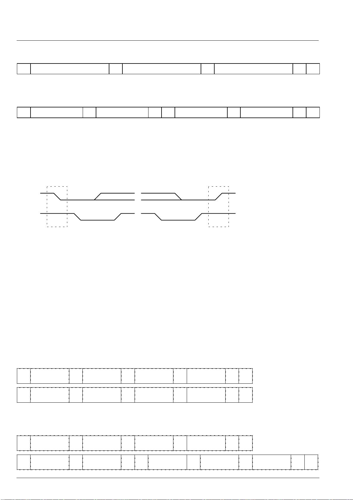
VPX 3225D, VPX 3224D
PRELIMINARY DATA SHEET
Write to Hardware Control Registers
S 1 0 0 0 0 1 1 0 ACK sub-addr ACK send data-byte ACK P
Read from Hardware Control Registers
S 1 0 0 0 0 1 1 0 ACK sub-addr ACK S 1 0 0 0 0 1 1 1 ACK receive data-byte NAK P
Note: S = I2C-Bus Start Condition
P = I
2
C-Bus Stop Condition
ACK = Acknowledge-Bit (active low on SDA from receiving device)
NAK = No Acknowledge-Bit (inactive high on SDA from receiving device)
SDA
1
0
SP
SCL
Fig. 2–40: I
2
C bus protocol (MSB first)
2.14.5. FP Control and Status Registers
Due to the internal architecture of the VPX, the IC cannot
2
react immediately to all I
C requests which interact with
the embedded processor (FP). The maximum response
timing is appr. 20 ms (one TV field) for the FP processor
if TV standard switching is active. If the addressed processor is not ready for further transmissions on the I
2
bus, the clock line SCL is pulled low. This puts the cur-
rent transmission into a wait state called clock synchronization. After a certain period of time, the VPX releases
the clock and the interrupted transmission is carried on.
Before accessing the address or data registers for the
FP interface (FPRD, FPWR, FPDAT), make sure that
the busy bit of FP is cleared (FPSTA).
C
Write to FP
S 1 0 0 0 0 1 1 0 ACK FPWR ACK send FP-address-
S 1 0 0 0 0 1 1 0 ACK FPDAT ACK send data-byte
byte high
high
ACK send FP-address-
ACK send data-byte
byte low
low
ACK P
ACK P
Read from FP
S 1 0 0 0 0 1 1 0 ACK FPRD ACK send FP-address-
S 1 0 0 0 0 1 1 0 ACK FPDAT ACK S 1 0 0 0 0 1 1 1 ACK receive data-byte
byte high
ACK send FP-address-
byte low
high
ACK P
ACK receive data-byte
low
NAK P
36 Micronas
Page 37
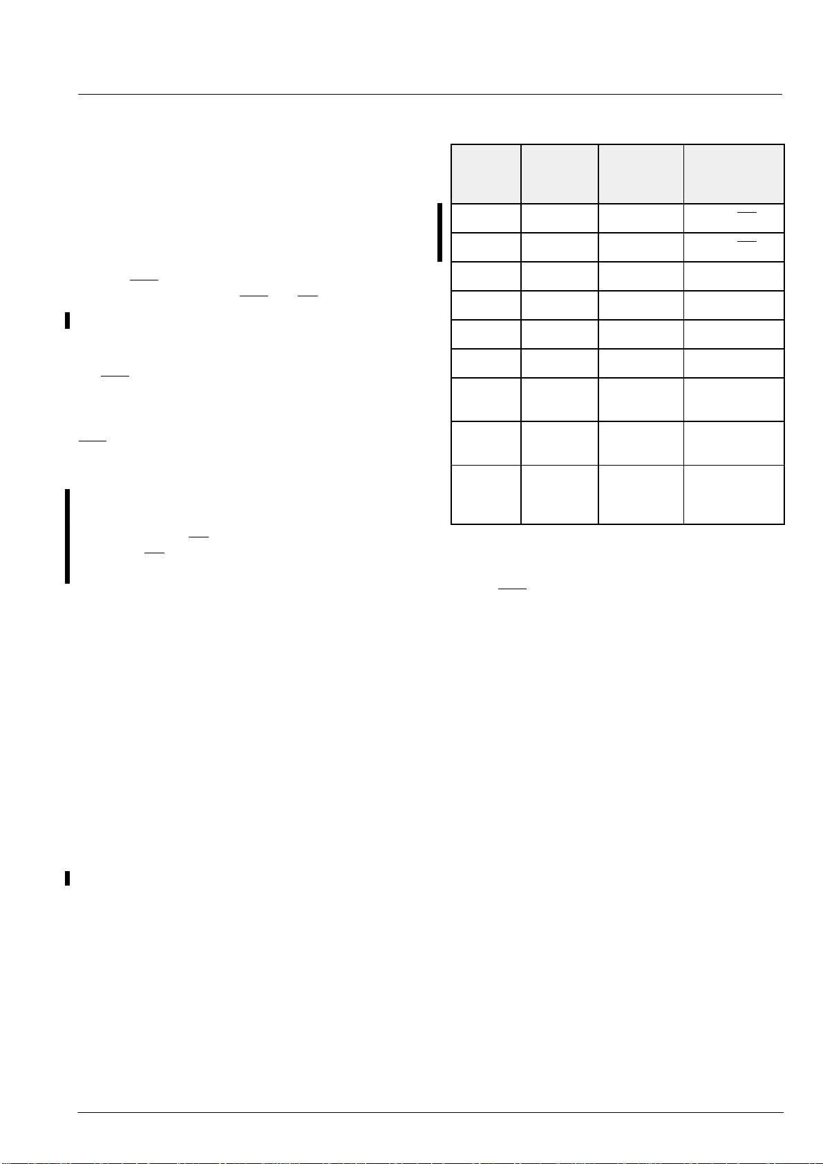
VPX 3225D, VPX 3224DPRELIMINARY DATA SHEET
2.15. Initialization of the VPX
2.15.1. Power-on-Reset
In order to completely specify the operational mode of
the VPX, appropriate values must be loaded into the I
2
and FP registers. After powering the VPX, an internal
power-on-reset clears all the FP/I
2
C-Registers. An ini-
tialization routine loads the default values for both the
2
I
C and FP registers from internal program ROM. The
external RES
inactive going edge of the RES
pin forces all outputs to be tri-stated. At the
pin, OE and FIELD are
read in for configuration. The FIELD pin is internally
pulled down, an external pull-up resistor could be used
to define a different power-on configuration. The poweron configuration is read on every rising edge of the external RES
pin.
Either inactive (tri-state) or active output pins could be
chosen with the FIELD pin at the inactive going edge of
RES
. In the inactive state, all relevant output pins are tristated, this includes Port A, Port B, HREF , VREF , FIELD,
VACT, PIXCLK, LLC, and LLC2. In the active setup, all
of these pins are driven. Table 2–16 gives an overview
of the different setups. Additionally , the data ports A and
B can be tri-stated with an external pullup resistor at the
output enable pin OE. The ports can be reactivated either by the OE pin or via setting bit 7 in I2C register 0xF2
(”oeq_dis”).
The VPX always comes up in NTSC square pixel mode
(640x240, both fields). In the case of inactive low power
mode, the internal H-Sync scheduler is switched off, as
in normal low power mode. After enabling the chip via
2
I
C Interface, the H-Sync scheduler is enabled and the
chips goes into a normal active NTSC operation condition.
2.15.2. Software Reset
The VPX provides the possibility of a software reset generated via I
2
C command (I2C register 0xAA, bit 2). Be
aware that this software reset does not activate the configuration read-in during power-on reset.
2.15.3. Low Power Mode
The VPX goes into low power mode, if the inactive mode
has been chosen. This is equal to the manual chosen
low-power mode. Note, that every manual selection of
the power mode (full or low-power) overwrites (resets!)
the power-up configuration. However, the current configuration cannot be read via the corresponding I
2
C register. Other restrictions are that the selection of the lowpower mode limits the rate of the I
2
C-interface to
100 kHz, and that the IC comes up with full power consumption until the low-power circuit becomes active.
Table 2–16: State of the pins during and after reset
Pins Reset
Active
Inactive
Setup
(FIELD=0)
Active
Setup
(FIELD=1)
C
Port A Tri-State Tri-State active (OE=0)
Port B Tri-State Tri-State active (OE=0)
HREF Tri-State Tri-State active
VREF Tri-State Tri-State active
FIELD pull down Tri-State active
VACT Tri-State Tri-State active
PIXCLK Tri-State Tri-State active
13.5 MHz
LLC Tri-State Tri-State active
27 MHz
TDO/
LLC2
Tri-State Tri-State active
programmable output
With the FIELD pin pulled down at the inactive going
edge of RES
, the VPX comes up in the low power mode.
This mode is introduced for power consumption critical
applications. It can be turned on and off with bit[1:0] in
2
the I
C register 0xAA (”lowpow”). There are three levels
of low power mode. When any of them is turned on, the
VPX waits for at least one complete video scan line in order to complete all internal tasks and then goes into tristate mode. The exact moment is not precisely defined,
so care should be taken to deactivate the system using
VPX data before the end of the video scan line in which
the VPX is switched into low power mode. During the low
power mode, all the I
2
C and FP registers are preserved,
so that the VPX restores its normal operation as soon as
low power mode is turned off, without need for any re-initialization. On the other hand, all the I
2
C and FP registers can be read/written as usual. The only exception is
the third level (value of 3 in I
power. In that mode, I
2
C speeds above 100 kbit/sec are
not allowed. In modes 1 and 2, I
2
C register 0xAA) of low
2
C can be used up to the
full speed of 400 kbit/s.
37Micronas
Page 38

VPX 3225D, VPX 3224D
PRELIMINARY DATA SHEET
2.16. JTAG Boundary-Scan, Test Access Port (TAP)
The design of the Test Access Port, which is used for
Boundary-Scan Test, conforms to standard IEEE
1 149.1-1990, with one exception. Also included is a list
of the mandatory instructions supported, as well as the
optional instructions. The following comprises a brief
overview of some of the basics, as well as any optional
features which are incorporated. The IEEE 1 149.1 document may be necessary for a more concise description.
Finally, an adherence section goes through a checklist
of topics and describes how the design conforms to the
standard.
The implementation of the instructions HIGHZ and
CLAMP conforms to the supplement P1 149.1/D11 (October 1992) to the standard 1149.1-1990.
2.16.1. General Description
The T AP in the VPX is incorporated using the four signal
interface. The interface includes TCK, TMS, TDI, and
TDO. The optional TRESET signal is not used. This is
not needed because the chip has an internal power-onreset which will automatically steer the chip into the
TEST-LOGIC-RESET state. The goal of the interface is
to provide a means to test the boundary of the chip.
There is no support for internal or BIST(built-in self test).
The one exception to IEEE 1 149.1 is that the TDO output
is shared with the LLC2 signal. This was necessitated
due to I/O restrictions on the chip (see section 2.16.3.
“Exceptions to IEEE 1149.1” for more information).
2.16.2.2. Instruction Register
The instruction register chooses which one of the data
registers is placed between the TDI and TDO pins when
the select data register state is entered in the T AP controller. When the select instruction register state is active, the instruction register is placed between the TDI
and TDO.
Instructions
The following instructions are incorporated:
– bypass
– sample/preload
– extest
– master mode
– ID code
– HIGHZ
– CLAMP
2.16.2.3. Boundary Scan Register
The boundary scan register (BSR) consists of boundary
scan cells (BSCs) which are distributed throughout the
chip. These cells are located at or near the I/O pad. It allows sampling of inputs, controlling of outputs, and shifting between each cell in a serial fashion to form the BSR.
This register is used to verify board interconnect.
Input Cell
2.16.2. TAP Architecture
The T AP function consists of the following blocks: TAPcontroller, instruction register, boundary-scan register,
bypass register, optional device identification register,
and master mode register.
2.16.2.1. TAP Controller
The TAP controller is responsible for responding to the
TCK and TMS signals. It controls the transition between
states of this device. These states control selection of
the data or instruction registers, and the actions which
occur in these registers. These include capture, shifting,
and update. See Fig. 5–1 of IEEE 1 149.1 for TAP state
diagram.
The input cell is constructed to achieve capture only.
This is the minimal cell necessary since Internal Test
(INTEST) is not supported. The cell captures either the
system input in the CAPTURE-DR state or the previous
cells output in the SHIFT-DR state. The captured data is
then available to the next cell. No action is taken in the
UPDA TE-DR state. See Figure 10–11 of IEEE 1 149.1 for
reference.
Output Cell
The output cell will allow both capture and update. The
capture flop will obtain system information in the CAPTURE-DR state or previous cells information in the
SHIFT-DR state. The captured data is available to the
next cell. The captured or shifted data is downloaded to
the update flop during the UPDA TE-DR state. The data
from the update flop is then multiplexed to the system
output pin when the EXTEST instruction is active. Otherwise, the normal system path exists where the signal
from the system logic flows to the system output pin. See
Fig. 10–12 of IEEE 1149.1 for reference.
38 Micronas
Page 39
VPX 3225D, VPX 3224DPRELIMINARY DATA SHEET
Tristate Cell
Each group of output signals, which are tristatable, is
controlled by a boundary scan cell (output cell type).
This allows either the normal system signal or the
scanned signal to control the tristate control. In the VPX,
there are four such tristate control cells which control
groups of output signals (see section “Output Driver Tristate Control” for further information).
Bidirect Cell
The bidirect cell is comprised of an input cell and a tristate cell as described in the IEEE standard. The signal
PIXCLK is a bidirectional signal.
2.16.2.4. Bypass Register
This register provides a minimal path between TDI and
TDO. This is required for complicated boards where
many chips may be connected in serial.
2.16.2.5. Device Identification Register
This is an optional 32-bit register which contains the
Micronas identification code (JEDEC controlled), part
and revision number. This is useful in providing the tester with assurance that the correct part and revision are
inserted into a PCB.
2.16.4. IEEE 1149.1-1990 Spec Adherence
This section defines the details of the IEEE1149.1 design for the VPX. It describes the function as outlined by
IEEE1149.1, section 12.3.1. The section of that document is referenced in the description of each function.
2.16.4.1. Instruction Register
(Section 12.3.1.b.i of IEEE 1149.1-1990)
The instruction register is three bits long. No parity bit is
included. The pattern loaded in the instruction register
during CAPTURE-IR is binary “101” (MSB to LSB). The
two LSBs are defined by the spec to be “01” (bit 1 and
bit 0) while the MSB (bit 2) is set to “1”.
2.16.4.2. Public Instructions
(Section 12.3.1.b.ii of IEEE 1149.1-1990)
A list of the public instructions is as follows:
Instruction Code (MSB to LSB)
EXTEST 000
SAMPLE/PRELOAD 001
2.16.2.6. Master Mode Data Register
This is an optional register used to control an 8-bit test
register in the chip. This register supports shift and update. No capture is supported. This was done so the last
word can be shifted out for verification.
2.16.3. Exception to IEEE 1149.1
There is one exception to IEEE 1149.1. The exception
is to paragraphs 3.1.1.c., 3.5.1.b, and 5.2.1.d (TESTLOGIC-RESET state). Because of pin limitations on the
chip, a pin is shared for two functions. When the circuit
is in the TEST-LOGIC-RESET state, the LLC2 signal is
driven out the TDO/LLC2 pin. When the circuit leaves
the TEST-LOGIC-RESET state, the TDO signal is driven
on this line. As long as the circuit is not in the TEST-LOGIC-RESET state, all the rules for application of the TDO
signal adhere to the IEEE1149.1 spec.
Since the VPX uses the JTAG function as a boundaryscan tool, the VPX does not sacrifice test of this pin since
it is verified by exercising JTAG function. The designer
of the PCB must make careful note of this fact, since he
will not be able to scan into chips receiving the LLC2 signal via the VPX. The PCB designer may want to put this
chip at the end of the chain or bring the VPX TDO out
separately and not have it feed another chip in a chain.
ID CODE 010
MASTER MODE 011
HIGHZ 100
CLAMP 110
BYPASS 100 – 111
The EXTEST and SAMPLE/PRELOAD instructions
both apply the boundary scan chain to the serial path.
The ID CODE instruction applies the ID register to the
serial chain. The BYP ASS, the HIGHZ, and the CLAMP
instructions apply the bypass register to the serial chain.
The MASTER MODE instruction is a test data instruction
for public use. It provides the ability to control an 8-bit
test register in the chip.
39Micronas
Page 40

VPX 3225D, VPX 3224D
PRELIMINARY DATA SHEET
2.16.4.3. Self-Test Operation
(Section 12.3.1.b.iii of IEEE 1149.1-1990).
There is no self-test operation included in the VPX de-
sign which is accessible via the TAP.
2.16.4.4. Test Data Registers
(Section 12.3.1.b.iv of IEEE 1149.1-1990).
The VPX includes the use of four test data registers.
They are the required bypass and boundary scan registers, the optional ID code register, and the master mode
register.
The bypass register is, as defined, a 1-bit register accessed by codes 100 through 111, inclusive. Since the
design includes the ID code register, the bypass register
is not placed in the serial path upon power-up or TestLogic-Reset.
The master mode is an 8-bit test register which is used
to force the VPX into special test modes. This is reset
upon power-on-reset. This register supports shift and
update only . It is not recommended to access this register. The loading of that register can drive the IC into an
undefined state.
2.16.4.5. Boundary Scan Register
(Section 12.3.1.b.v of IEEE 1149.1-1990)
The boundary scan chain has a length of 38 shift regis-
ters. The scan chain order is specified in the section “Pin
Connections”.
2.16.4.6. Device Identification Register
(Section 12.3.1.b.vi of IEEE 1149.1-1990)
The manufacturer’s identification code is “6C”
(hex)
for
Micronas. The general implementation scheme uses
only the 7 LSBs and excludes the MSB, which is the parity bit. The part number is “7230”
VPX 3225D and “7231”
version code starts from “1”
. in case of VPX 3224D. The
(hex)
and changes with every
(hex)
. in case of
(hex)
revision. The version number relates to changes of the
chip interface only.
2.16.4.7. Performance
(Section 12.3.1.b.vii of IEEE 1149.1-1990)
See section “Specification” for further information.
Version Part Number Manufacturer ID
31 28 27 12 11 1 0
7F
87
272300d9
Fig. 2–41: Device identification register
10001010001101000000000001101 001
40 Micronas
Page 41
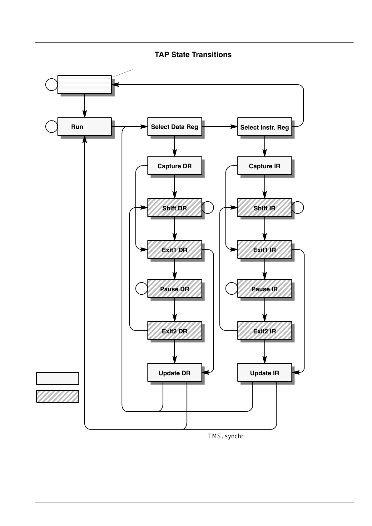
КККККК
КККККК
TAP State Transitions
VPX 3225D, VPX 3224DPRELIMINARY DATA SHEET
1
Test-Logic-Reset
0
0
Run / Idle
$F
$C
TDO could be used as programmable output pin or LLC2
clock signal (see Pin Description).
$7
1
Select Data Reg
11
Select Instr. Reg
0
$6
11
Capture DR
Capture IR
0
$2
Shift DR
00
11
$1
Exit1 DR
11
$4
0
$E
0
$A
Shift IR
$9
Exit1 IR
State Code
TDO inactive
TDO active
0
$3
00
Pause DR
Pause IR
11
$0
Exit2 DR
00
Exit2 IR
11
$5
Update DR
TMS=1 TMS=1
TMS=0 TMS=0
Update IR
State transitions are dependend on the value of TMS, synchronized by TCK.
$B
$8
$D
Fig. 2–42: TAP state transitions
41Micronas
Page 42

VPX 3225D, VPX 3224D
––*************************************************************
––
–– This is the BSDL for the 44-Pin Version of the VPXD design.
––
––*************************************************************
Library IEEE;
Use work.STD_1149_1_1990.ALL;
Entity VPXD_44 is
Generic (Physical_Pin_Map:string := ”UNDEFINED”);
Port( ––define ports
TDI,TCK,TMS: in bit;
TDO,HREF,VREF,FIELD: out bit;
A: out bit_vector(7 downto 0);
PVDD,PVSS: linkage bit;
PIXCLK: out bit;
OEQ: in bit;
LLC, VACT: out bit;
B: out bit_vector(7 downto 0);
SDA,SCL: inout bit;
VSS,XTAL2,XTAL1,VDD: linkage bit;
RESQ: in bit;
AVDD,AVSS,VRT,ISGND: linkage bit;
CIN,VIN1,VIN2,VIN3: in bit
);
PRELIMINARY DATA SHEET
Attribute Pin_Map of VPXD_44 : Entity is Physical_Pin_Map;
constant Package_44 : Pin_Map_String := ––map pins to signals
”TDI : 1 ” &
”TCK : 2 ” &
”TDO : 3 ” &
”HREF : 4 ” &
”VREF : 5 ” &
”FIELD : 6 ” &
”A : (7,8,9,10,14,15,16,17)” &
”PVDD : 11 ” &
”PIXCLK : 12 ” &
”PVSS : 13 ” &
”OEQ : 18 ” &
”LLC : 19 ” &
”VACT : 20 ” &
”B : (21,22,23,24,25,26,27,28),” &
”SDA : 29 ” &
”SCL : 30 ” &
”RESQ : 31 ” &
”VSS : 32 ” &
”VDD : 33 ” &
”XTAL2 : 34 ” &
”XTAL1 : 35 ” &
”AVDD : 36 ” &
”CIN : 37 ” &
”AVSS : 38 ” &
”VIN1 : 39 ” &
”VIN2 : 40 ” &
”VRT : 41 ” &
”VIN3 : 42 ” &
”ISGND : 43 ” &
”TMS : 44 ” ;
Attribute Tap_Scan_In of TDI : signal is true; ––define JTAG Controls
Attribute Tap_Scan_Mode of TMS : signal is true;
Attribute Tap_Scan_Out of TDO : signal is true;
Attribute Tap_Scan_Clock of TCK : signal is (10.0e6,Both); ––max frequency and levels TCK can be stopped at.
Attribute Instruction_Length of VPXD_44: entity is 3; ––define instr. length
Attribute Instruction_Opcode of VPXD_44: entity is
”EXTEST (000),” & ––External Test
42 Micronas
Page 43

VPX 3225D, VPX 3224DPRELIMINARY DATA SHEET
”SAMPLE (001),” & ––Sample/Preload
”IDCODE (010),” & ––ID Code
”MASTERMODE (011),” & ––Master Mode (internal Test)
”HIGHZ (100),” & –– Highz
”CLAMP” (110),” & –– Clamp
”BYPASS (100,101,110,111),”; ––Bypass
Attribute Register_Access of VPXD_44: entity is ––instr. vs register
”BOUNDARY (EXTEST,SAMPLE),” & ––control
”BYPASS (BYPASS, HIGHZ, CLAMP),” &
”IDCODE[32] (IDCODE),” &
”MASTERMODE[8] (MASTERMODE) ”;
Attribute INSTRUCTION_Capture of VPXD_44: entity is ”101”; ––captured instr.
Attribute IDCODE_Register of VPXD_44: entity is
”0001” & ––initial rev
”0100011010000000” & ––part numb. 7230
”0000” & ––7F Count
”1101100” & ––Micronas Code–Parity
”1”; ––Mandatory LSB
Attribute Boundary_Cells of VPXD_44: entity is ”BC_1,BC_4”; –-BC_1 for output cell
––BC_4 for input cell
Attribute Boundary_Length of VPXD_44: entity is 38; ––Boundary scan length
Attribute Boundary_Register of VPXD_44: entity is ––Boundary scan defin.
–– num cell port function safe ccel disval rslt
” 37 (BC_4, VIN3, input, X ),” &
” 36 (BC_4, VIN2, input, X ),” &
” 35 (BC_4, VIN1, input, X ),” &
” 34 (BC_4, CIN, input, X ),” &
” 33 (BC_1, *, internal, X ),” & ––low power mode
” 32 (BC_4, RESQ, input, X ),” &
” 31 (BC_4, SCL, input, X ),” &
” 30 (BC_1, SCL, output3, X, 30, 1, Z ),” & ––open collector
” 29 (BC_4, SDA, input, X ),” &
” 28 (BC_1, SDA, output3, X, 28, 1, Z ),” & ––open collector
” 27 (BC_1, B(0), output3, X, 19, 1, Z ),” &
” 26 (BC_1, B(1), output3, X, 19, 1, Z ),” &
” 25 (BC_1, B(2), output3, X, 19, 1, Z ),” &
” 24 (BC_1, B(3), output3, X, 19, 1, Z ),” &
” 23 (BC_1, B(4), output3, X, 19, 1, Z ),” &
” 22 (BC_1, B(5), output3, X, 19, 1, Z ),” &
” 21 (BC_1, B(6), output3, X, 19, 1, Z ),” &
” 20 (BC_1, B(7), output3, X, 19, 1, Z ),” &
” 19 (BC_1, *, control, X ),” & ––control
” 18 (BC_1, VACT, output3, X, 16, 1, Z ),” &
” 17 (BC_1, LLC, output3, X, 16, 1, Z ),” &
” 16 (BC_1, *, control, X ),” & ––control
” 15 (BC_4, OEQ, input, X ),” &
” 14 (BC_1, A(0), output3, X, 8, 1, Z ),” &
” 13 (BC_1, A(1), output3, X, 8, 1, Z ),” &
” 12 (BC_1, A(2), output3, X, 8, 1, Z ),” &
” 11 (BC_1, A(3), output3, X, 8, 1, Z ),” &
” 10 (BC_1, *, control, X ),” & ––control
” 9 (BC_1, PIXCLK,output3, X, 10, 1, Z ),” &
” 8 (BC_1, *, control, X ),” & ––control
” 7 (BC_1, A(4), output3, X, 8, 1, Z ),” &
” 6 (BC_1, A(5), output3, X, 8, 1, Z ),” &
” 5 (BC_1, A(6), output3, X, 8, 1, Z ),” &
” 4 (BC_1, A(7), output3, X, 8, 1, Z ),” &
” 3 (BC_1, *, control, X, , 1, Z ),” & ––control
” 2 (BC_1, FIELD, output3, X, 3, 1, Z ),” &
” 1 (BC_1, VREF, output3, X, 16, 1, Z ),” &
” 0 (BC_1, HREF, output3, X, 16, 1, Z ),”;
End VPXD_44;
43Micronas
Page 44

VPX 3225D, VPX 3224D
PRELIMINARY DATA SHEET
2.17. Enable/Disable of Output Signals
In order to enable the output pins of the VPX to achieve
the high impedance/tristate mode, various controls have
been implemented. The following paragraphs give an
overview of the different tristate modes of the output signals. It is valid for all output pins, except the XTAL2
(which is the oscillator output) and the VRT pin (which is
an analog reference voltage).
BS (Boundary Scan) Mode:
The tristate control by the test access port TAP for
boundary scan has the highest priority . Even if the T APcontroller is in the EXTEST or CLAMP mode, the tristate
behavior is only defined by the state of the different
boundary scan registers for enable control. If the TAP
controller is in HIGHZ mode, then all output pins are in
tristate mode independently of the state of the different
boundary scan registers for enable control.
RESET State:
If the T AP-controller is not in the EXTEST mode, then the
RESET -state defines the state of all digital outputs. The
only exception is made for the data output of the boundary scan interface TDO. If the circuit is in reset condition
(RES
= 0), then all output interfaces are in tristate mode.
2
C Control:
I
The tristate condition of groups of signals can also be
controlled by setting the I
is neither in EXTEST mode nor RESET state, then the
2
I
C-Register 0xF2 defines whether the output is in tristate condition or not (see “I
end”).
Output Enable Input OE
The output enable signal OE
put ports. If the previous three conditions do not cause
the output drivers to go into high impedance mode, then
the OE
data ports.
The OE
0xF2 [oeq_dis]. The OE signal will either directly connect the output drivers or it will be latched internally with
the LLC signal depending on I2C register 0xF2 [latoeq].
Additionally , a delay of 1 LLC clock cycle can be enabled
with I2C register 0xF2 [oeqdel].
signal defines the driving conditions of the video
pin function can be disabled via I2C register
2
C-Register 0xF2. If the circuit
2
C-Registers VPX Back-
:
only effects the video out-
Table 2–17: Output driver configuration
EXTEST RESET I2C OE# Driver Stages
active – – – Output driver stages are defined by the state of the different
boundary scan enable registers.
inactive active – – Output drivers are in high impedance mode.
inactive inactive = 0 – Output drivers are in high impedance mode. PIXCLK is working.
inactive inactive = 1 = 0 Output drivers HREF, VREF, FIELD, VACT, LLC, are working.
Outputs A[7:0] and B[7:0] are working
inactive inactive = 1 = 1 Output drivers HREF, VREF, FIELD, VACT, LLC, are working.
Output drivers of A[7:0] and B[7:0] are in high impedance mode.
Remark: EXTEST mode is an instruction conforming to the standard for Boundary Scan Test IEEE 1149.1 – 1990
44 Micronas
Page 45
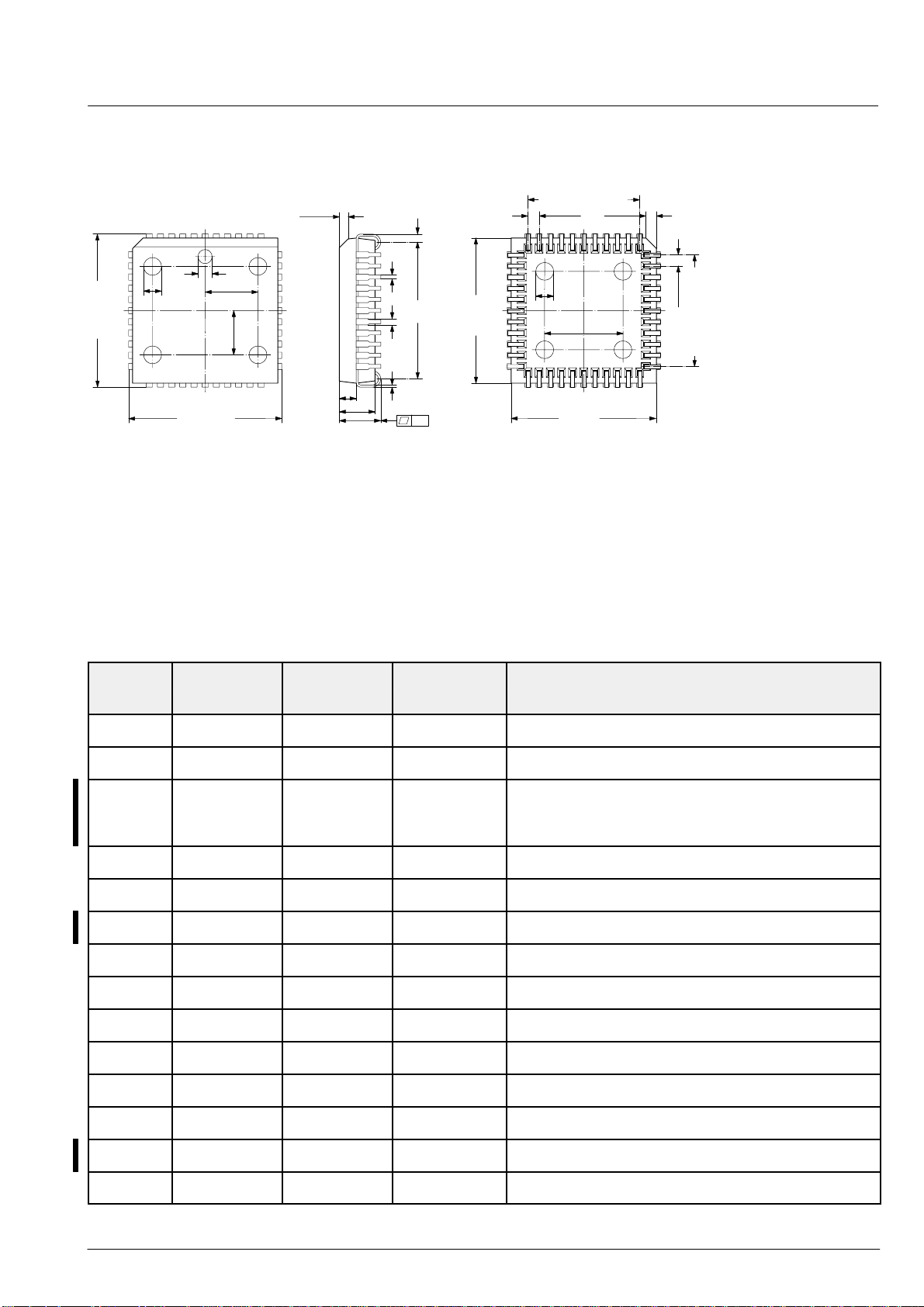
3. Specification
3.1. Outline Dimensions
6
140
VPX 3225D, VPX 3224DPRELIMINARY DATA SHEET
10 x 1.27 = 12.7
x 45 °1.1
1.27
0.1±
0.1±
1.2 x 45°
39
0.48
0.1
15.7 0.9
0.7110.27
29
2818
1.9
4.05
4.75
±0.15
0.07±
0.1
±
16.5
2
8.6
0.1±
16.5
0.125±
17.525
7
2
17
17.525
1.6
6
5
0.125±
Fig. 3–1:
44-Pin Plastic Leaded Chip Carrier Package
(PLCC44)
Weight approximately 2.5 g
Dimensions in mm
3.2. Pin Connections and Short Descriptions
NC = not connected; leave vacant
X = obligatory
Pin No. Pin Name Pin Type Connection Short Description
PLCC44 (if not used)
0.1±
1.27
SPGS7003-2/3E
0.1±
10 x 1.27 = 12.7
1 TDI IN NC Boundary-Scan-Test Data Input
2 TCK IN NC Boundary-Scan-Test Clock Input
3 TDO
LLC2
DACT
OUT NC Boundary-Scan-Test Data Output
LLC / 2 = 13.5MHz Output
Active VBI Data Qualifier Output
4 HREF OUT NC Horizontal Reference Output
5 VREF OUT NC Vertical Reference Output
6 FIELD OUT NC Odd/Even Field Identifier Output
7 A7 OUT NC Port A – Video Data Output
8 A6 OUT NC Port A – Video Data Output
9 A5 OUT NC Port A – Video Data Output
10 A4 OUT NC Port A – Video Data Output
11 PVDD SUPPLY X Supply Voltage Pad Circuits
12 PIXCLK OUT NC Pixel Clock Output
13 PVSS SUPPLY X Ground, Pad Circuits
14 A3 OUT NC Port A – Video Data Output
45Micronas
Page 46
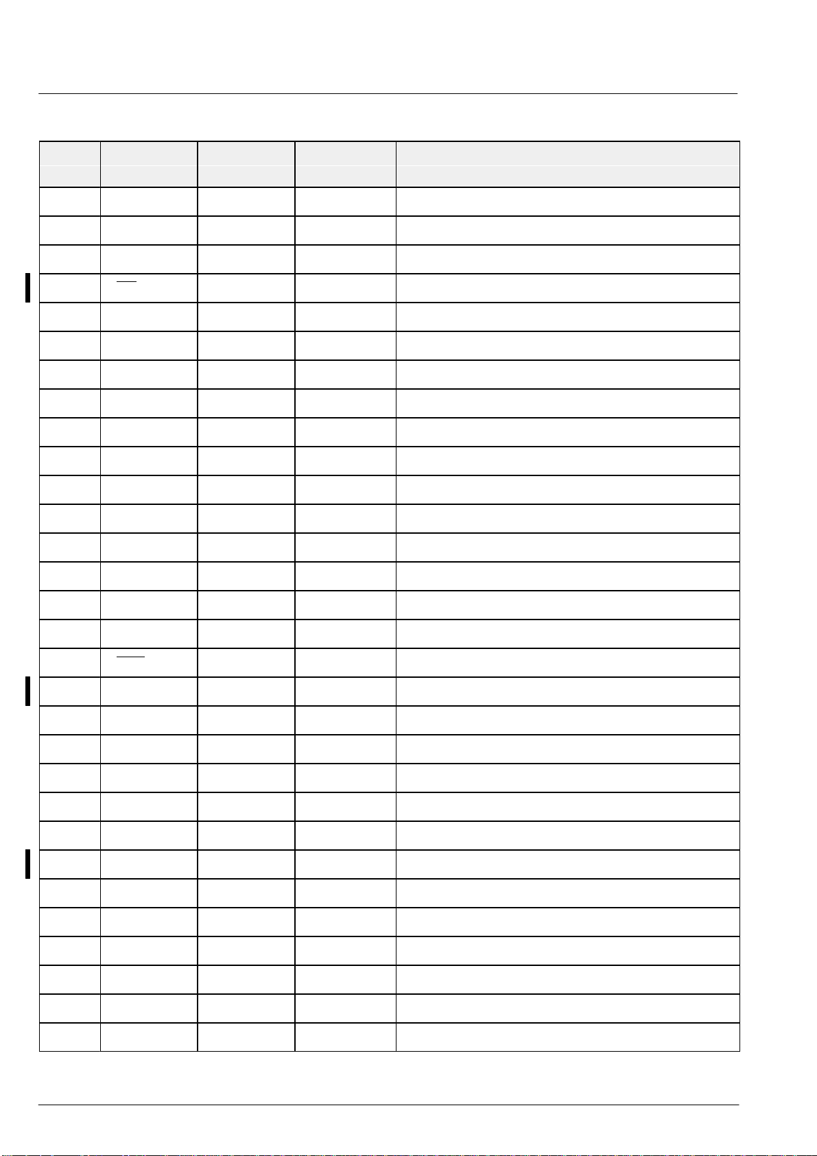
VPX 3225D, VPX 3224D
Pin Connections and Short Descriptions, continued
Pin No. Pin Name Type Connection Short Description
PLCC44 (if not used)
15 A2 OUT NC Port A – Video Data Output
16 A1 OUT NC Port A – Video Data Output
17 A0 OUT NC Port A – Video Data Output
18 OE IN VSS Output Ports Enable Input
19 LLC OUT NC PIXCLK * 2 = 27 MHz Output
20 VACT OUT NC Active Video Qualifier Output
21 B7 OUT NC Port B – Video Data Output
22 B6 OUT NC Port B – Video Data Output
23 B5 OUT NC Port B – Video Data Output
PRELIMINARY DATA SHEET
24 B4 OUT NC Port B – Video Data Output
25 B3 OUT NC Port B – Video Data Output
26 B2 OUT NC Port B – Video Data Output
27 B1 OUT NC Port B – Video Data Output
28 B0 OUT NC Port B – Video Data Output
29 SDA IN/OUT NC I2C Bus Data
30 SCL IN/OUT NC I2C Bus Clock
31 RES IN X Reset Input
32 VSS SUPPLY X Ground, Digital Circuitry
33 VDD SUPPLY X Supply Voltage, Digital Circuitry
34 XTAL2 OSC OUT X Analog Crystal Output
35 XTAL1 OSC IN X Analog Crystal Input
36 AVDD SUPPLY X Supply Voltage, Analog Circuitry
37 CIN AIN NC Analog Chroma Input
38 AVSS SUPPLY X Ground, Analog Circuitry
39 VIN1 AIN NC Analog Video 1 Input
40 VIN2 AIN NC Analog Video 2 Input
41 VRT Reference X Reference Voltage Top, Video ADC
42 VIN3 AIN NC Analog Video 3 Input
43 ISGND SUPPLY X Signal Ground, Analog Video Inputs
44 TMS IN NC Boundary-Scan-Test Mode Select
46 Micronas
Page 47

VPX 3225D, VPX 3224DPRELIMINARY DATA SHEET
3.3. Pin Descriptions
Pins 44, 1 – JTAG Input Pins, TMS, TDI (Fig. 3–4)
Test Mode Select and Test Data Input signals of the
JTAG Test Access Port (TAP). Both signals are inputs
with a TTL compatible input specification. To comply
with JTAG specification they use pull-ups at their input
stage. The input stage of the TMS and TDI uses a TTL
Schmitt Trigger.
Pin 2 – JTAG Input Pin, TCK (Fig. 3–3)
Clock signal of the Test-Access Port. It is used to synchronize all JT AG functions. When JTAG operations are
not being performed, this pin should be driven to VSS.
The input stage of the TCK uses a TTL Schmitt Trigger .
Pin 3 – JT AG Output Pin, TDO, LLC2, DACT (Fig. 3–6)
Data output for JT AG T est Access Port (T AP). Moreover,
if Test Access Port (TAP) is in Test-Logic-Reset State,
this pin can be used as output pin of the LLC2 clock signal (I2C Reg. 0xF2 bit[4] = 1) or it can be used as output
pin for the active VBI-Data signal DACT (see section
2.13.).
Pins 4 to 6 – Reference Signals, HREF, VREF, FIELD
(Fig. 3–6)
These signals are internally generated sync signals. The
state of FIELD during the positive edge of RES
the power up mode (see section 2.15.1.).
Pins 7 to 10, 14 to 17 – Video, Port A[7:0] (Fig. 3–6)
Video output port to deliver luma and/or chroma data.
Pin 11 – Supply Voltage (Pad Circuitry), PVDD
Pins 12, 19 – Pixel Clock, PIXCLK, LLC (Fig. 3–6)
PIXCLK and LLC are the reference clock signals for the
video data transmission ports A[7:0] and B[7:0].
Pin 13 – Ground (Pad Circuitry), PVSS
Pin 18 – Output Enable Input Signal, OE
The output enable input signal has TTL Schmitt Trigger
input characteristic. It controls the tri-state condition of
both video ports. The state during the positive edge of
RES
selects the I2C device address (see section
2.14.3.).
selects
(Fig. 3–3)
Pins 21 to 28 – Video, Port B[7:0] (Fig. 3–6)
Video output port to deliver chroma data. In 8-bit modes,
Port B can be activated as programmable output (see
section 2.6.3.).
Pin 29 – I2C Bus Data, SDA (Fig. 3–5)
This pin connects to the I
Pin 30 – I
This pin connects to the I
Pin 31 – Reset Input, RES
A low level on this pin resets the VPX 3225D.
Pin 32 – Ground (Digital Circuitry), VSS
Pin 33 – Supply Voltage (Digital Circuitry), VDD
Pins 34, 35 – Crystal Input and Output, XTAL1, XTAL2
(Fig. 3–8)
These pins are connected to a 20.25 MHz crystal oscillator which is digitally tuned by integrated shunt capacitances. An external clock can be fed into XT AL1. In this
case, clock frequency adjustment must be switched off.
Pin 36 – Supply Voltage (Analog Circuitry), AVDD
Pin 37 – Chroma Input, CIN (Fig. 3–12, Fig. 3–11)
This pin is connected to the S-VHS chroma signal. A resistive divider is used to bias the input signal to the
middle of the converter input range. CIN can only be
connected to the chroma (Video 2) A/D converter. The
signal must be AC-coupled.
Pin 38 – Ground (Analog Front-end), AVSS
Pins 39, 40, 42 – Video Input 1–3, VIN1–3 (Fig. 3–10)
These are the analog video inputs. A CVBS, S-VHS
luma signal is converted using the luma (Video 1) A/D
converter. The VIN1 input can also be switched to the
chroma (Video 2) ADC. The input signal must be ACcoupled.
Pin 41 – Reference Voltage Top, VRT (Fig. 3–9)
Via this pin, the reference voltage for the A/D converters
is decoupled. The pin is connected with 10 mF/47 nF to
the Signal Ground Pin.
2
C Bus Clock, SCL (Fig. 3–5)
2
C bus data line.
2
C bus clock line.
(Fig. 3–3)
Pins 20 – Video Qualifier Output, VACT (Fig. 3–6)
This pin delivers a signal which qualifies active video
samples.
Pin 43 – Ground (Analog Signal Input), ISGND
This is the high-quality ground reference for the video
input signals.
47Micronas
Page 48
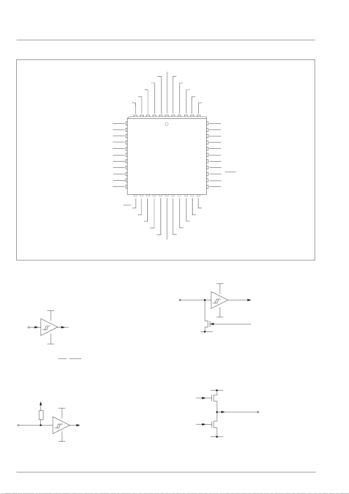
VPX 3225D, VPX 3224D
3.4. Pin Configuration
TDO (LLC2, DACT)
HREF
VREF
FIELD
TCK
PRELIMINARY DATA SHEET
TDI
TMS
ISGND
VIN3
VRT
VIN2
PIXCLK
Fig. 3–2: 44-pin PLCC package.
3.5. Pin Circuits
A7
A6
A5
A4
PVDD
PVSS
A3
A2
A1
A0
6 5 4 3 2 14443424140
7
8
9
10
11
12
13
14
15
16
17
VPX 3225D
VPX 3224D
Top View
18 19 20 21 22 23 24 25 26 27 28
OE
LLC
VACT
B7
B6
B5
B4
B3
B2
34
B1
39
38
37
36
35
VIN1
AVSS
CIN
AVDD
XTAL1
XTAL2
33
32
31
30
29
VDD
VSS
RES
SCL
SDA
B0
VDD
VDD
Pin
VSS
Fig. 3–3: TCK, OE, RES
PVDD
VDD
Pin
VSS
Fig. 3–4: TMS, TDI
Pin
VSS
Fig. 3–5: I2C Interface SDA, SCL
The characteristics of the Schmitt Triggers are depend
on the supply of VDD/VSS.
PVDD
P
OUT
Pin
N
PVSS
Fig. 3–6: A[7:0], B[7:0], HREF, VREF, LLC,
PIXCLK, VACT, TDO
48 Micronas
Page 49
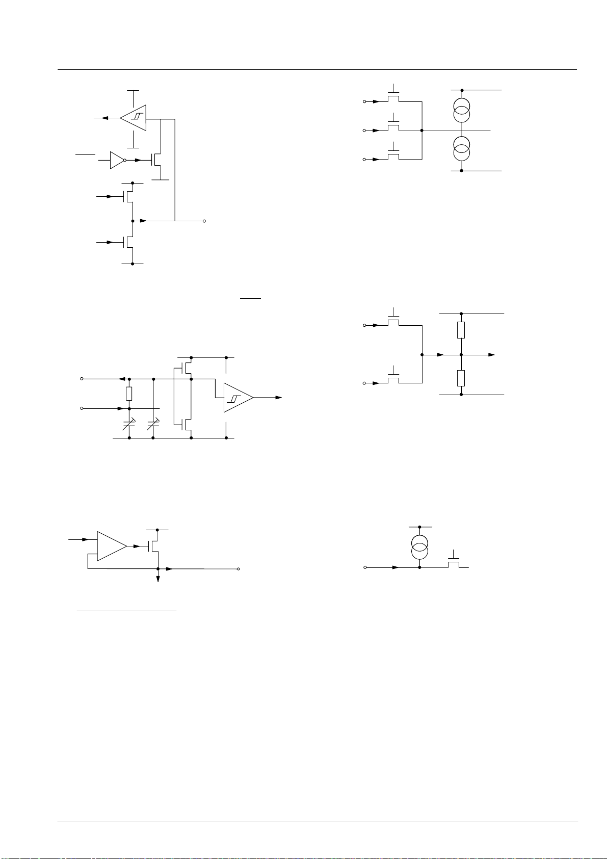
VPX 3225D, VPX 3224DPRELIMINARY DATA SHEET
VDD
RES
VSS
PVDD
P
FIELD
Pin
N
PVSS
Fig. 3–7: Reference Signal FIELD and wake-up
selection LOWPOW on positve edge of RES
AVDD
XTAL2
0.5M
XTAL1
P
f
ECLK
N
AVSS
VIN1
VIN2
VIN3
N
N
N
clamping
Fig. 3–10: Video Inputs ADC1
VIN1
CIN
N
N
bias
Fig. 3–11: Video Inputs ADC2
AVDD
To ADC1
AVSS
AVDD
To ADC2
AVSS
Fig. 3–8: Crystal Oscillator
AVDD
BIAS
–
+
P
ADC Reference
AVSS
Fig. 3–9: Reference Voltage VR T
VRT
VRT
VIN1,
VIN2,
VIN3,
off
CIN
Fig. 3–12: Unselected Video Inputs
49Micronas
Page 50

VPX 3225D, VPX 3224D
4. Electrical Characteristics
4.1. Absolute Maximum Ratings
PRELIMINARY DATA SHEET
Symbol Parameter Pin
Name
T
A
T
S
T
J
V
SUB
P
TOT MAX
Ambient Temperature 0 65 °C
Storage Temperature –40 125 °C
Junction Temperature 0 125 °C
Supply Voltage, all Supply Inputs –0.3 6 V
Power Dissipation due to package
characteristics
VDD,
PVDD,
AVDD
Input Voltage of FIELD, TMS, TDI PVSS – 0.5 PVDD + 0.5
Input Voltage TCK PVSS – 0.5 6 V
Input Voltage SDA,
SCL
Signal Swing A[7:0],
B[7:0],
PIXCLK,
HREF,
VREF,
FIELD,
VACT,
LLC,
TDO
Min. Max. Unit
1170 mW
1)
V
VSS – 0.5 6 V
PVSS – 0.5 PVDD + 0.5
1)
V
Maximum D | VDD – AVDD |
Maximum D | VSS – PVSS |
0.5 V
0.1 V
Maximum D | VSS – AVSS |
Maximum D | PVSS – AVSS |
1)
External voltage exceeding PVDD+0.5 V should not be applied to these pins even when they are tri-stated.
Stresses beyond those listed in the “Absolute Maximum Ratings” may cause permanent damage to the device. This
is a stress rating only . Functional operation of the device at these or any other conditions beyond those indicated in the
“Recommended Operating Conditions/Characteristics” of this specification is not implied. Exposure to absolute maximum ratings conditions for extended periods may affect device reliability.
50 Micronas
Page 51
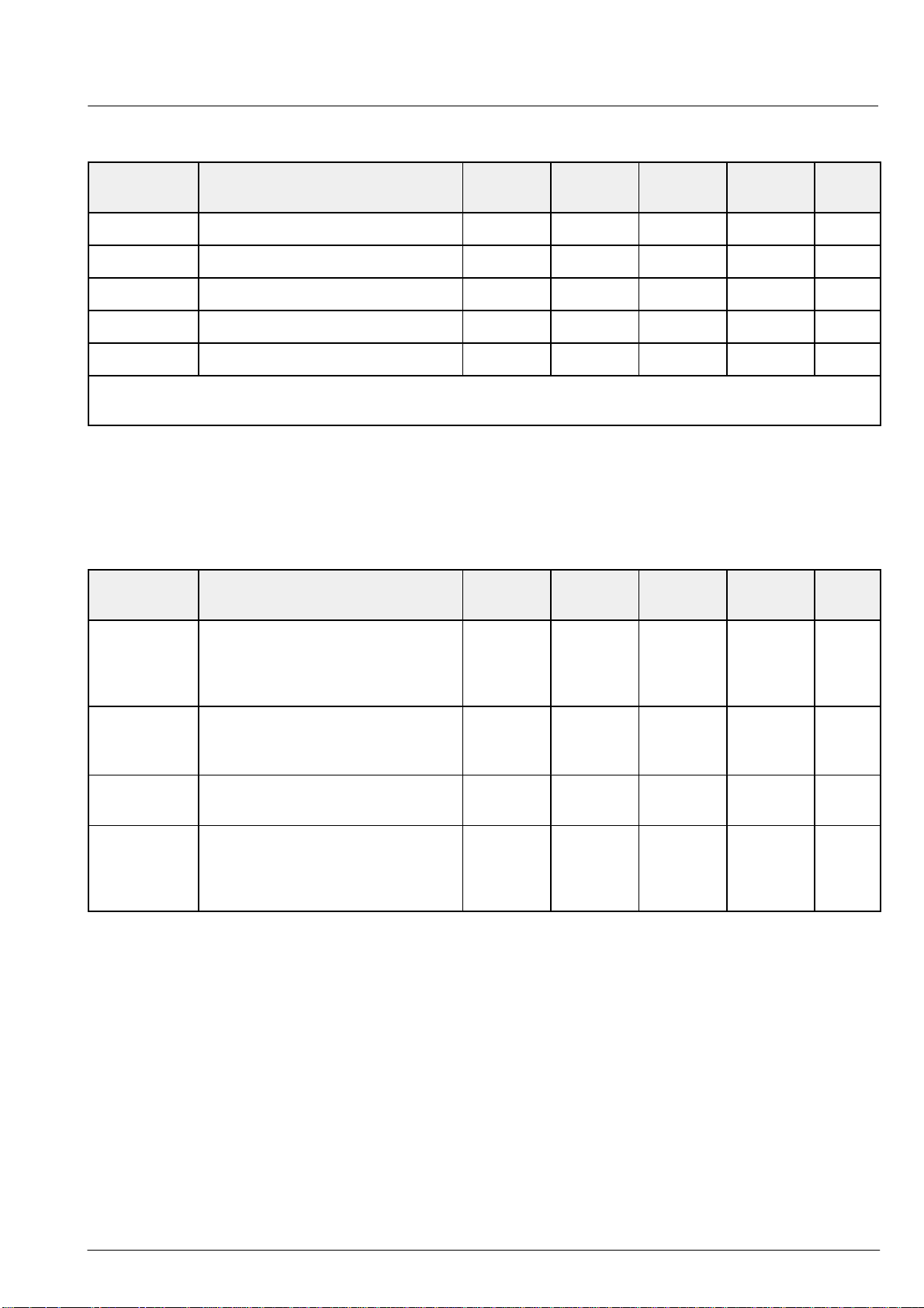
4.2. Recommended Operating Conditions
VPX 3225D, VPX 3224DPRELIMINARY DATA SHEET
Symbol Parameter Pin
Min. Typ. Max. Unit
Name
T
A
V
SUPA
V
SUPD
V
SUPP
f
XTAL
1)
could also be connected to the 5 V supply net; but for best performance, it is recommended to connect it to 3.3 V
Ambient Operating Temperature – 0 – 65 °C
Analog Supply Voltage AVDD 4.75 5.0 5.25 V
Digital Supply Voltage VDD 4.75 5.0 5.25 V
Pad Supply Voltage PVDD 3.15 3.6
1)
Clock Frequency XTAL1/2 20.250 MHz
supply (see Fig. 7–1).
4.2.1. Recommended Analog Video Input Conditions
Symbol Parameter Pin
Min. Typ. Max. Unit
Name
V
V
VIN
Analog Input Voltage VIN1,
0 – 3.5 V
VIN2,
VIN3,
CIN
C
CP
Input Coupling Capacitor
Video Inputs
VIN1,
VIN2,
680 nF
VIN3
C
CP
Input Coupling Capacitor
CIN 1 nF
Chroma Input
R
PD
Recommended Drive Impedance VIN1,
75 100
W
VIN2,
VIN3,
CIN
51Micronas
Page 52
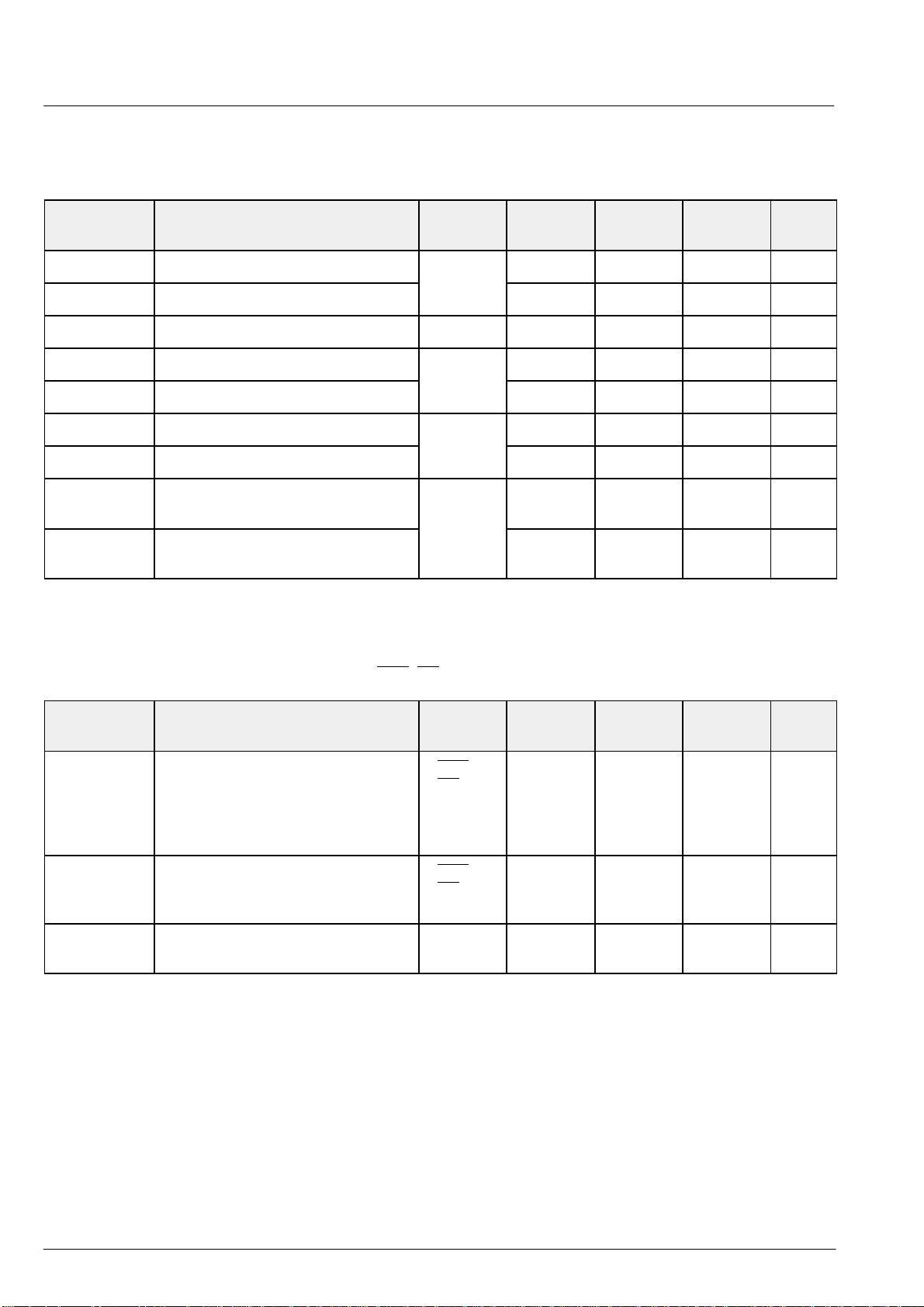
VPX 3225D, VPX 3224D
SDA
SDA
4.2.2. Recommended I2C Conditions
(Timing diagram see Fig. 5–3 on page 61)
PRELIMINARY DATA SHEET
Symbol Parameter Pin
Name
V
V
f
SCL
t
I2C1
t
I2C2
t
I2C3
t
I2C4
t
I2C5
t
I2C6
IMIL
IMIH
I2C-BUS Input Low Voltage SCL,
I2C-BUS Input High Voltage
I2C-BUS Frequency SCL 100 kHz
I2C START Condition Setup Time SCL,
I2C STOP Condition Setup Time
I2C-Clock Low Pulse Time SCL 5000 ns
I2C-Clock High Pulse Time 5000 ns
I2C-Data Setup Time Before
Rising Edge of Clock
SCL,
SDA
I2C-Data Hold Time after Falling
Edge of Clock
Min. Typ. Max. Unit
0.3 VDD
0.6 VDD
1200 ns
1200 ns
55 ns
55 ns
4.2.3. Recommended Digital Inputs Levels of RES, OE, TCK, TMS, TDI
Symbol Parameter Pin
Min. Typ. Max. Unit
Name
V
IL
Input Voltage LOW RES,
OE
,
–0.5 0 0.8 V
TCK,
TMS,
TDI
V
IH
Input Voltage HIGH RES,
OE
,
2.0 5 6 V
TCK
V
IH
Input Voltage HIGH TDI,
2.0 PVDD PVDD +
TMS
V
0.3
52 Micronas
Page 53
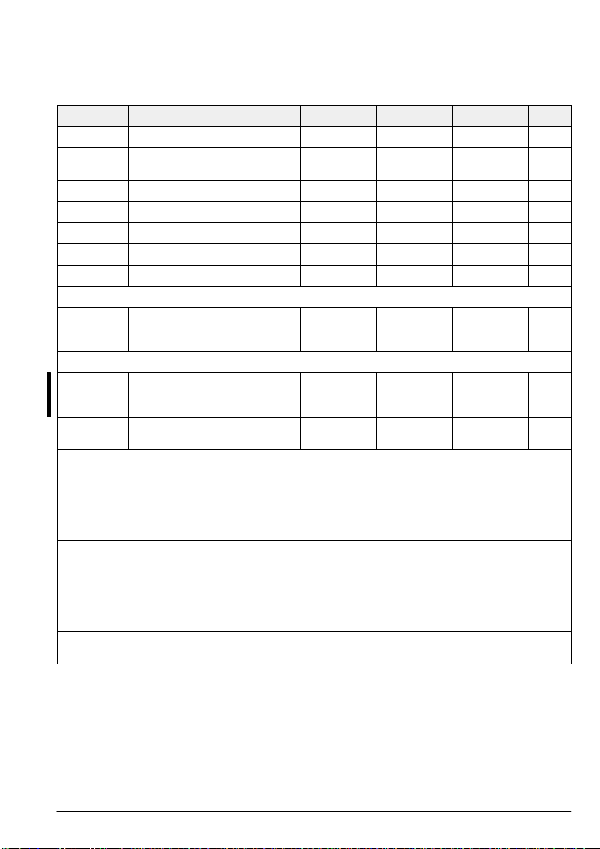
VPX 3225D, VPX 3224DPRELIMINARY DATA SHEET
4.2.4. Recommended Crystal Characteristics
Symbol Parameter Min. Typ. Max. Unit
T
A
f
P
Operating Ambient Temperature 0 – 65 °C
Parallel Resonance Frequency
with Load Capacitance C
DfP/f
DfP/f
R
R
C
0
C
1
P
P
Accuracy of Adjustment – – ±20 ppm
Frequency Temperature Drift – – ±30 ppm
Series Resistance – – 25
Shunt Capacitance 3 – 7 pF
Motional Capacitance 20 – 30 fF
Load Capacitance Recommendation
C
Lext
External Load Capacitance
pins to Ground (PLCC44)
(pin names: Xtal1 Xtal2)
DCO Characteristics
C
ICLoadmin
2)
Effective Load Capacitance @ min.
DCO-Position, Code 0,
package: PLCC44
C
ICLoadrng
Effective Load Capacitance Range,
DCO Codes from 0..255
= 13 pF
L
1
)
from
– 20.250000
– MHz
fundamental
W
– 4.7 – pF
3 4.3 5.5 pF
8.7 12.7 16.7 pF
1)
Remarks on defining the External Load Capacitance:
External capacitors at each crystal pin to ground are required. They are necessary to tune the effective load
capacitance of the PCBs to the required load capacitance (C
lower the clock frequency results. The nominal free running frequency should match f
) of the crystal. The higher the capacitors, the
L
= 20.25 MHz. Due to
p
different layouts of customer PCBs, the matching capacitor size should be determined in the application. The
suggested value is a figure based on experience with various PCB layouts.
Tuning condition: Code DVCO Register = –720
2)
Remarks on Pulling Range of DCO:
The pulling range of the DCO is a function of the used crystal and effective load capacitance of the IC (C
+ C
LoadBoard
1 + 0.5 * [ C
f
= fP * –––––––––––––––––––––––
L
1 + 0.5 * [ C
3)
Remarks on DCO Codes:
). The resulting frequency (fL) with an effective load capacitance of C
/ (C0 + CL ) ]
1
/ (C0 + C
1
Leff
) ]
Leff
= C
ICLoad
+ C
ICLoad
LoadBoard
The DCO hardware register has 8 bits; the FP control register uses a range of –2048...2047.
is
53Micronas
Page 54
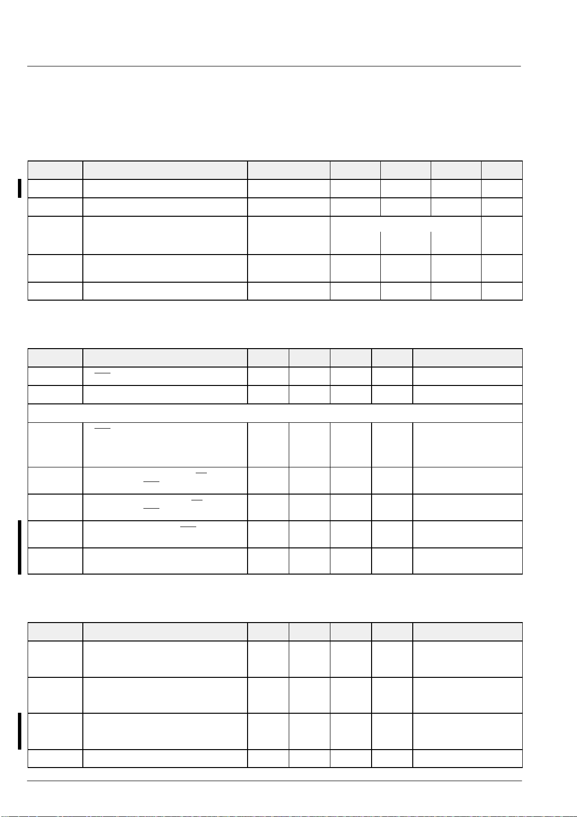
VPX 3225D, VPX 3224D
PRELIMINARY DATA SHEET
4.3. Characteristics
at T
= 0 to 65 °C, V
A
= 60 °C, V
at T
C
SUPD/A
SUPD/A
= 4.75 to 5.25 V, V
= 5 V, V
SUPP
= 3.15 to 3.5 V, f = 20.25 MHz for min./max. values
SUPP
= 3.3 V, f = 20.25 MHz for typical values
4.3.1. Current Consumption
Symbol Parameter Pin Name Min. Typ. Max. Unit
I
VSUPA
I
VSUPD
I
VSUPP
P
TOT
P
TOT
Current Consumption AVDD 25 40 53 mA
Current Consumption VDD 80 100 135 mA
Current Consumption PVDD application dependent mA
Total Power Dissipation,
normal operation condition
Total Power Dissipation, low power mode AVDD, VDD, PVDD 0.1 W
AVDD, VDD, PVDD 0.95 W
75@5V
4.3.2. Characteristics, Reset
Symbol Parameter Min. Typ. Max. Unit Test Conditions
t
RES MIN
t
RES INT
Default Wake-up Selection (see timing diagram in section 5.1. on page 60)
t
RES MIN
RES Low Pulse to initiate an internal reset 50 ns xtal osc. is working
Internal Reset Hold Time 3.2 µs xtal osc. is working
RES Low Pulse due to the time needed to
discharge pin FIELD by the internal pulldown transistor for default selection
(see schematic of fig. 3–7)
1 ms xtal osc. is working
C
I
leak
LOAD
< 10 mA
(FIELD) < 50 pF
t
s-WU
t
h-WU
I
PD
R
PU
Setup Time of pin FIELD and OE
to posedge of RES
Hold Time of pin FIELD and OE
to posedge of RES
Pull-down current during RES = 0 at pin
FIELD
Recommended Pull-up resistor to enforce a
logical 1 to pin FIELD
20 ns
20 ns
42 75 68
10
mA
kW
V
FIELD
= 5V
4.3.3. XTAL Input Characteristics
Symbol Parameter Min. Typ. Max. Unit Test Conditions
V
I
t
Startup1
t
Startup2
Clock Input Voltage, XTAL1 1.3 V
Oscillator Startup Time at VDD
Slew-rate of 1 V / 1 µs
(see section 5.1. on page 60)
Reset Hold Time after
the Oscillator is active
(see section 5.1. on page 60)
5.0
0.4 1.0 ms
ms
PP
capacitive coupling of
XTAL1,
XTAL 2 remains open
k
XTAL
Duty Cycle 50 %
54 Micronas
Page 55
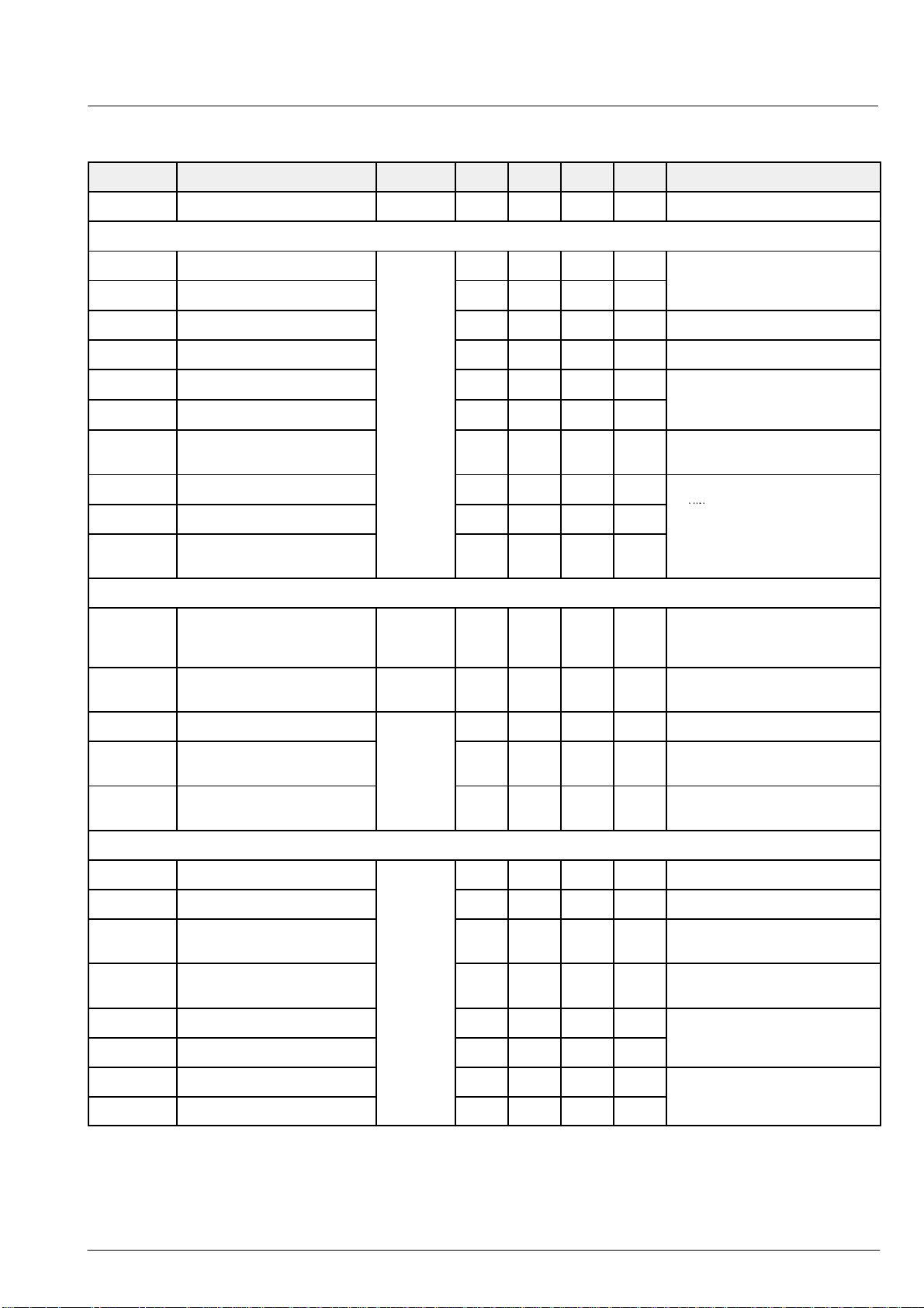
VPX 3225D, VPX 3224DPRELIMINARY DATA SHEET
VIN2
f
MHz
V
V
VIN1
VIN2
CIN
DC-ramp
DC-Ramp
4.3.4. Characteristics, Analog Front-End and ADCs
Symbol Parameter Pin Name Min. Typ. Max. Unit Test Conditions
V
VRT
Reference Voltage Top VRT 2.5 2.61 2.72 V
10 mF//10 nF, 1 GW Probe
Luma – Path
R
VIN
C
VIN
V
VIN
V
VIN
Input Resistance VIN1,
1
,
Input Capacitance
VIN3
5 pF
Full Scale Input Voltage 1.86 1.93 2.0 V
Full Scale Input Voltage 0.5 0.6 0.7 V
MW
Code clamp – DAC = 0
min. AGC Gain
PP
max. AGC Gain
PP
AGC AGC step width 0.145 0.163 0.181 dB 6-bit resolution = 63 Steps
= 1
= 1.5
,
DNL
V
VINCL
Q
CL
I
CL–LSB
DNL
AGC
ICL
sig
AGC Differential Non-Linearity ±0.5 LSB
– 2 dBr of max. AGC Gain
Input Clamping Level, CVBS 1.0 V Binary Level = 68 LSB
min. AGC Gain
Clamping DAC Resolution –16 15 steps 6 Bit – I–DAC, bipolar
Input Clamping Current per step 0.7 1 1.3
Clamping DAC Differential
±0.5 LSB
mA
VIN
Non-Linearity
Chroma – Path
R
CIN
Input Resistance
SVHS Chroma
CIN,
VIN1
1.4 2.0 2.6
kW
C
VIN
V
CIN
V
CINDC
Input Capacitance CIN,
VIN1
Full Scale Input Voltage, Chroma CIN,
Input Bias Level,
SVHS Chroma
Binary Code for Open
5 pF
1.08 1.14 1.2 V
– 1.5 – V
128
PP
Chroma Input
Dynamic Characteristics for all Video-Paths (Luma + Chroma)
BW Bandwidth VIN1,
10 14 MHz –2 dBr input signal level
,
XTALK Crosstalk, any two video inputs
THD Total Harmonic Distortion
VIN3,
–56 –48 dB 1 MHz, –2 dBr signal level
–48 –45 dB 1 MHz, 5 harmonics,
–2 dBr signal level
SINAD Signal to Noise and
Distortion Ratio
42 46 dB 1 MHz, all outputs,
–2 dBr signal level
INL Integral Non-Linearity, ±1.3 ±2.4 LSB Code Density,
p
DNL Differential Non-Linearity ±0.5 ±0.85 LSB
DG Differential Gain ±3 % –12 dBr, 4.4 MHz signal on
p
DP Differential Phase 1.5 deg
55Micronas
Page 56
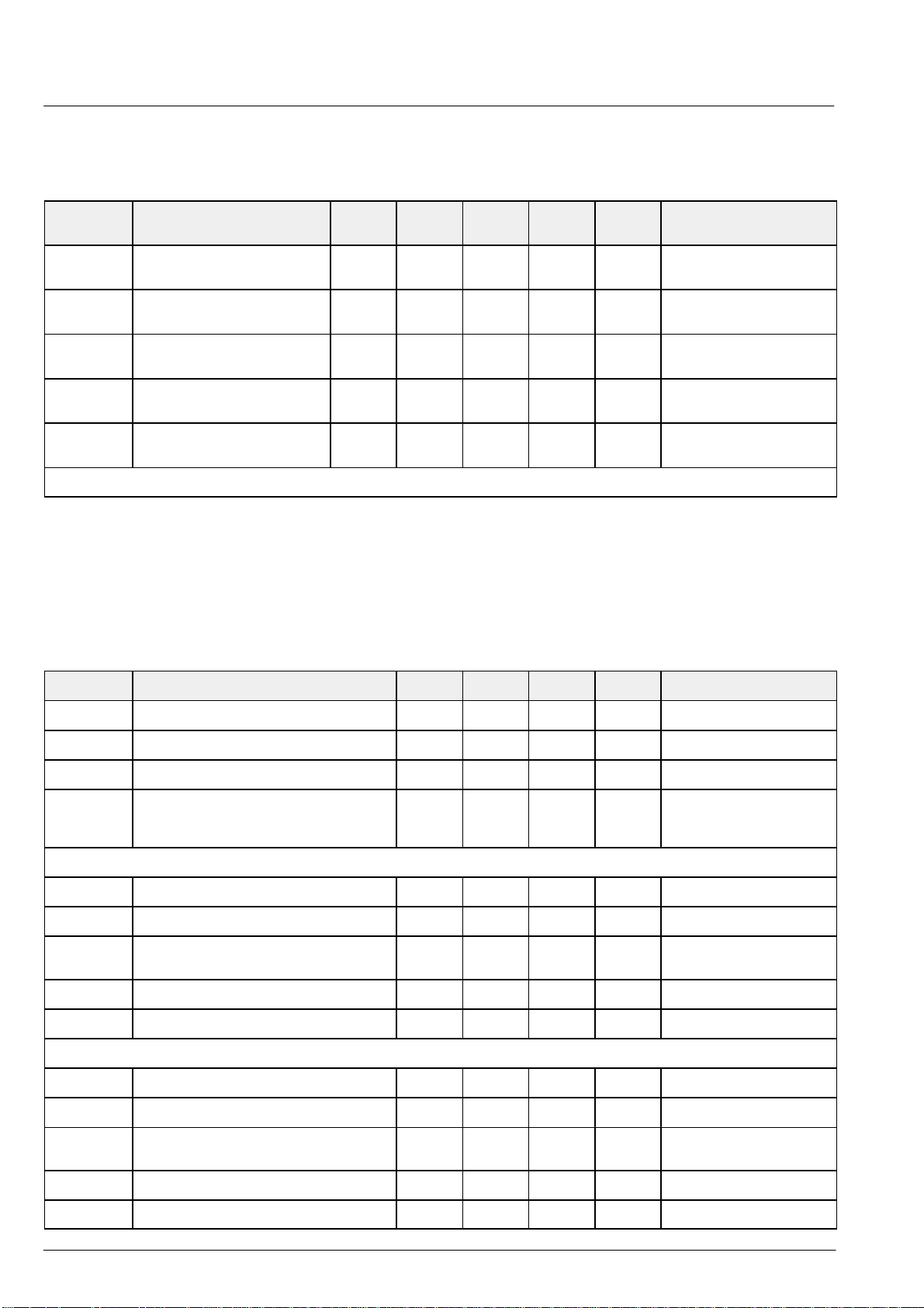
VPX 3225D, VPX 3224D
4.3.5. Characteristics, Control Bus Interface
(Timing diagram see Fig. 5–3 on page 61)
PRELIMINARY DATA SHEET
Symbol Parameter Pin
Min. Typ. Max. Unit Test Conditions
Name
V
IMOL
t
IMOL1
t
IMOL2
t
F
f
SCL
1)
The maximum clock frequency of the I2C interface is limited to 100 kHz while the IC is working in the low power mode.
Output Low Voltage SDA,
SCL
I2C-Data Output Hold Time after
SDA 15 ns
Falling Edge of Clock SCL
I2C-Data Output Setup Time be-
SDA 100 ns f
fore Rising Edge of Clock SCL
Signal Fall Time SDA,
SCL
Clock Frequency
1)
SCL 0 – 100
– – 0.4
0.6
V
V
– – 300 ns C
kHz
1000
kHz
4.3.6. Characteristics, JTAG Interface (Test Access Port TAP)
(Timing diagram see Fig. 5–5 on page 63)
Il = 3 mA
I
= 6 mA
l
= 1 MHz, VDD = 5 V
SCL
= 400 pF,
L
R
= 4,7 k
PU
low power mode
normal operating condition
Symbol Parameter Min. Typ. Max. Unit Test Conditions
F
CYCL-TAP
F
H-TAP
F
L-TAP
V
RES-TAP
JTAG Cycle Time 100 ns
TCK High Time 50 ns
TCK Low Time 50 ns
Minimum supply voltage to initiate an
3.5 V VDD pin
internal reset of the JTAG-TAP generated
by a voltage supply supervision circuit
Test Access Port (TAP), see timing diagram (Fig. 5–5 on page 63)
t
S-TAP
t
H-TAP
t
D-TAP
t
ON-TAP
t
OFF-TAP
TMS, TDI Setup Time 12 ns
TMS, TDI Hold Time 12 ns
TCK to TDO Propagation Delay
50 ns
for Valid Data
TDO Turn-on Delay 45 ns
TDO Turn-off Delay 45 ns
Boundary-Scan Test, Characteristics of all IO pins which are connected to the boundary scan register chain
t
S-PINS
t
H-PINS
Input Signals Setup Time at CAPTURE-DR 10 ns
Input Signals Hold Time at CAPTURE-DR 10 ns
t
D-PINS
t
ON-PINS
t
OFF-PINS
TCK to Output Signals,
50 ns
Delay for Valid Data
Turn-on Delay 20 ns
Turn-off Delay 20 ns
56 Micronas
Page 57
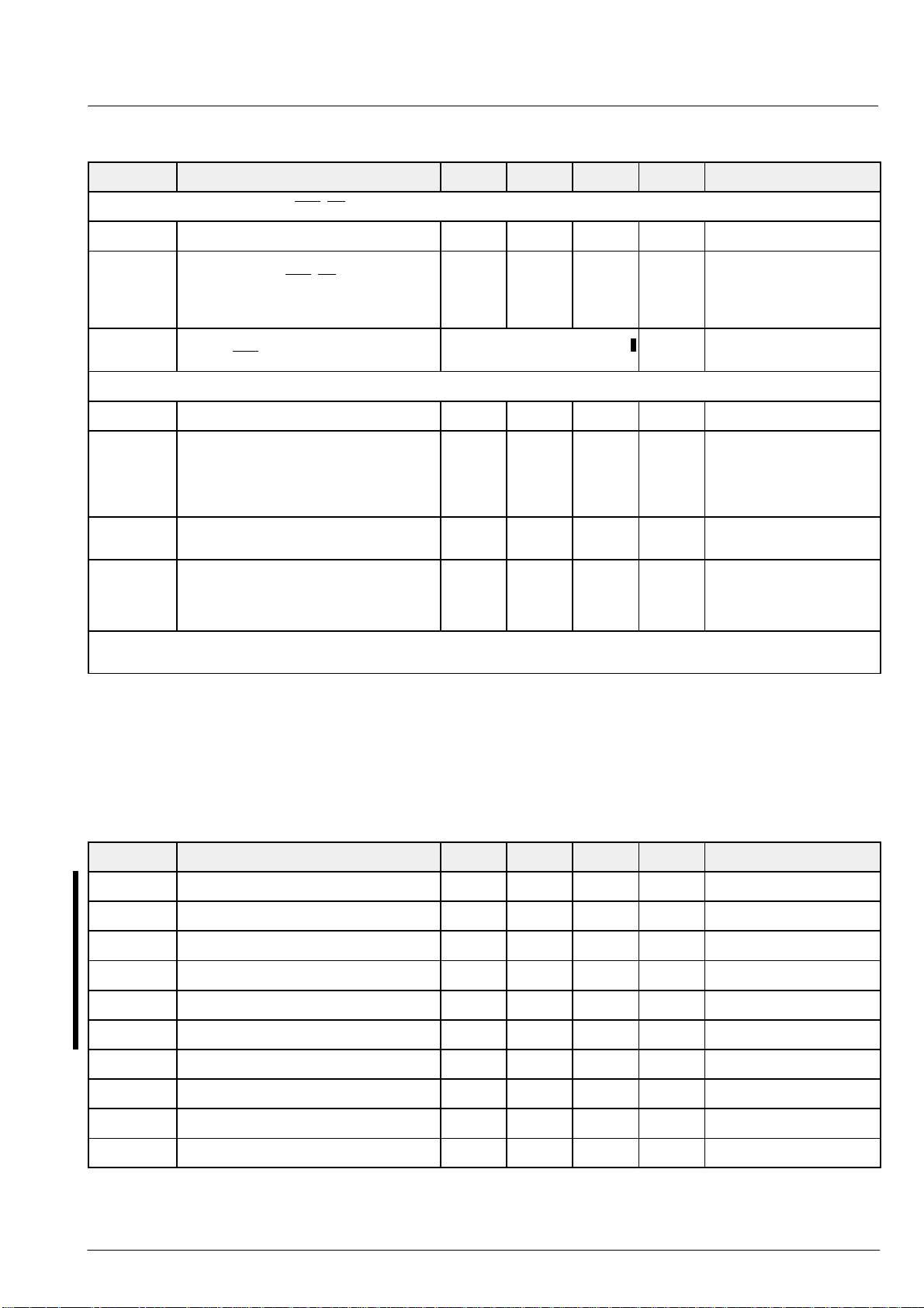
VPX 3225D, VPX 3224DPRELIMINARY DATA SHEET
4.3.7. Characteristics, Digital Inputs/Outputs
Symbol Parameter Min. Typ. Max. Unit Test Conditions
Digital Input Pins TMS, TDI, TCK, RES, OE, SCL, SDA
C
IN
I
I
I
I
I
PD
Input Capacitance 5 8 pF
Input Leakage Current
Input Pins TCK, RES
, OE, SCL, SDA
Input Leakage Current
Input Pins with Pull-ups: TDI and TMS
Pull-down Current at Pin FIELD
during RES
= 0 for Default Selection
–25 –55
see section 4.3.2.
–1
+1
+1
mA
mA
VI = V
VI≤V
VI = V
VI≤V
SS
DD
SS
DD
Digital Output pins A[7:0], B[7:0], HREF, VREF, FIELD, VACT, LLC, PIXCLK, TDO
C
O
V
OL
V
OL
V
OH
I
O
High-Impedance Output Capacitance 5 8 pF
Output Voltage LOW
0.6 V
(all digital output pins except SDA, SCL)
Output Voltage LOW
(only SDA, SCL)
Output Voltage HIGH
2.4 – PVDD V
0.4
0.6
V
V
(all digital output pins except SDA, SCL)
Output Leakage Current
–1
+1
mA
mA
Il = 3 mA
I
= 6 mA
l
while IC remains in low
power mode
VI = V
SS
VI≤V
DD
A special VDD, VSS supply is used only to support the digital output pins. This means, inherently, that in case of tri-state conditions,
external sources should not drive these signals above the voltage PVDD which supplies the output pins.
4.3.8. Clock Signals PIXCLK, LLC, and LLC2
The following timing specifications refer to the timing diagrams of section 5.7.1. on page 64.
Symbol Parameter Min. Typ. Max. Unit Test Conditions
t
LLC
F
LLC
t
LLC2
F
LLC2
t
PIXCLK
F
PIXCLK
t
HCLK1
t
DCLK1
t
HCLK2
t
DCLK2
LLC Cycle Time 37 ns
LLC Duty Cycle FH / (F
L +
F
)
H
50 %
LLC2 Cycle Time 74 ns
LLC2 Duty Cycle FH / (F
L +
F
)
H
50 %
PIXCLK Cycle Time 74 ns
PIXCLK Duty Cycle FH / (F
L +
F
)
H
50 %
Output Signal Hold Time for LLC2 0 ns
Propagation Delay for LLC2 10 ns
Output Signal Hold Time for PIXCLK 10 ns
Propagation Delay for PIXCLK 18 ns
57Micronas
Page 58
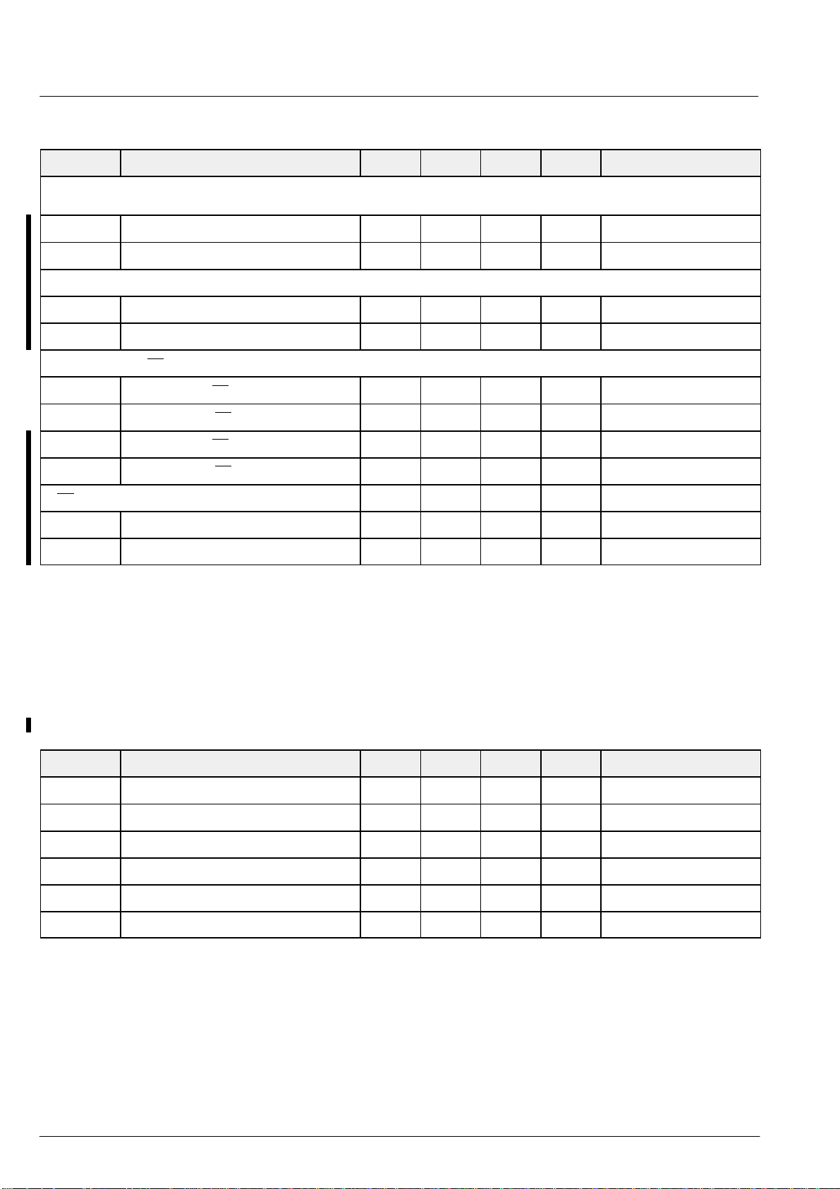
VPX 3225D, VPX 3224D
PRELIMINARY DATA SHEET
4.3.9. Digital Video Interface
Symbol Parameter Min. Typ. Max. Unit Test Conditions
Data and Control Pins (LLC to A[7:0], B[7:0], HREF, VREF, FIELD, VACT:
The following timing specifications refer to the timing diagrams of section 5.7. on page 64.
t
OH
t
PD
Output Hold Time 20 ns I2C Reg. h’AA –bit[6]=1
Propagation Delay 35 ns
New LLC output timing (available starting version D4)
t
OH
t
PD
Output Hold Time 8 ns I2C Reg. h’AA –bit[6]=0
Propagation Delay 23 ns
Output Enable by OE (For more information, see section 5.4. on page 62)
t
ON
t
OFF
t
ON1
t
OFF1
Output Enable OE of A[7:0], B[7:0] 15 ns
Output Disable OE of A[7:0], B[7:0] 15 ns
Output Enable OE of A[7:0], B[7:0] 5 ns
Output Disable OE of A[7:0], B[7:0] 5 ns
OE input timing
t
SU
t
HD
input data set-up time 11 ns
input data hold time 3 ns
4.3.10. Characteristics, TTL Output Driver
Output Pins A[7:0], B[7:0], PIXCLK, LLC, VACT, HREF, VREF, FIELD, TDO/LLC2
Symbol Parameter Min. Typ. Max. Unit Test Conditions
t
RA
t
FA
IOH(0) Output High Current (strength = 0) –1.37 –2.25 –2.87 mA VOH = 0.6 V
IOL(0) Output Low Current (strength = 0) 1.75 3.5 4.5 mA VOH = 2.4 V
IOH(7) Output High Current (strength = 7) –11 –18 –25 mA VOH = 0.6 V
IOL(7) Output Low Current (strength = 7) 14 28 36 mA VOH = 2.4 V
Rise Time 2 5 10 ns Cl = 30 pF, strength = 4
Fall Time 2 5 10 ns C
= 30 pF, strength = 4
l
58 Micronas
Page 59
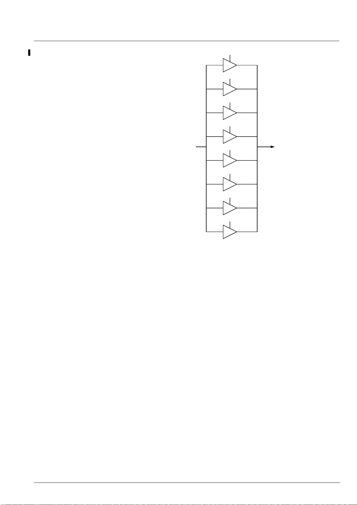
VPX 3225D, VPX 3224DPRELIMINARY DATA SHEET
4.3.10.1. TTL Output Driver Description
The driving capability/strength is controlled by the state
of the two I
2
C registers F8
and F9
hex
hex
.
A special PVDD, PVSS supply is used only to support
the digital output pins. This means, inherently, that in
case of tri-state conditions, external sources should not
drive these signals above the voltage PVDD which supplies the output pins.
All timing specifications are based on the following assumptions:
– the load capacitance of the fast pins (output driver ty-
pe A) is C
= 30 pF,
A
– the load capacitance of the remaining pins (output
driver type B) is C
= 50 pF,
B
– no static currents are assumed,
– the driving capability of the pads is STR = 4, which
means that 5 of 8 output drivers are enabled.
The typical case specification relates to:
– the ambient temperature is T
to a junction temperature of T
= 25 °C, which relates
A
= 70 °C;
J
– the power supply of the pad circuits is PVDD = 3.3 V,
and the power supply of the digital parts is VDD =
5.0 V.
The best case specification relates to:
– a junction temperature of T
= 0 °C,
J
– the power supply of the pad circuits is PVDD = 3.6 V,
and the power supply of the digital parts is VDD =
5.25 V.
The worst case specification relates to:
– a junction temperature of T
= 125 °C,
J
– the power supply of the pad circuits is PVDD = 3.0 V,
and the power supply of the digital parts is VDD =
4.75 V.
strength = 7
strength w 6
strength w 5
strength w 4
strength w 3
strength w 2
strength w 1
strength w 0
Fig. 4–1: Block diagram of the output stages
Note: The drivers of the output pads are implemented
as a parallel connection of 8 tri-state buffers of the
same size. The buffers are enabled depending on the
desired driver strength. This opportunity offers the advantage of adapting the driver strength to on-chip and
off-chip constraints, e.g. to minimize the noise resulting from steep signal transitions.
Rise times are specified as a transition between 0.6 V to
2.4 V. Fall times are defined as a transition between
2.4 V to 0.6 V.
59Micronas
Page 60
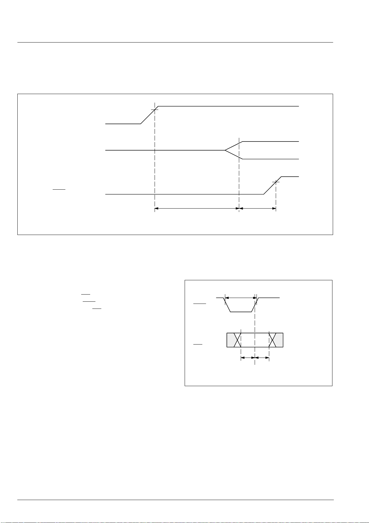
VPX 3225D, VPX 3224D
PRELIMINARY DATA SHEET
5. Timing Diagrams
5.1. Power-Up Sequence
The reset should not reach high level before the oscillator has started. This requires a reset delay of >1 ms (see Fig.5–1).
Supplies
Crystal
Oscillator
RES
Fig. 5–1: Power-up sequence
5.2. Default Wake-up Selection
The state of FIELD and OE
(inactive) going edge of RES
two power-on parameters. OE
pins are sampled at the high
in order to select between
determines the I2C ad-
dress.
95%
t
STARTUP1
RES
t
RES MIN
t
STARTUP2
V
IOH
V
IOH
V
IOL
The FIELD pin is internally pulled down. An external pullup resistor defines a different power on configuration.
FIELD defines the global wake-up mode of the VPX.
With FIELD pulled down, the VPX goes into low power
FIELD
OE
t
s-WU
t
h-WU
V
IOH
V
IOL
mode.
Fig. 5–2: Default wake-up selection
60 Micronas
Page 61
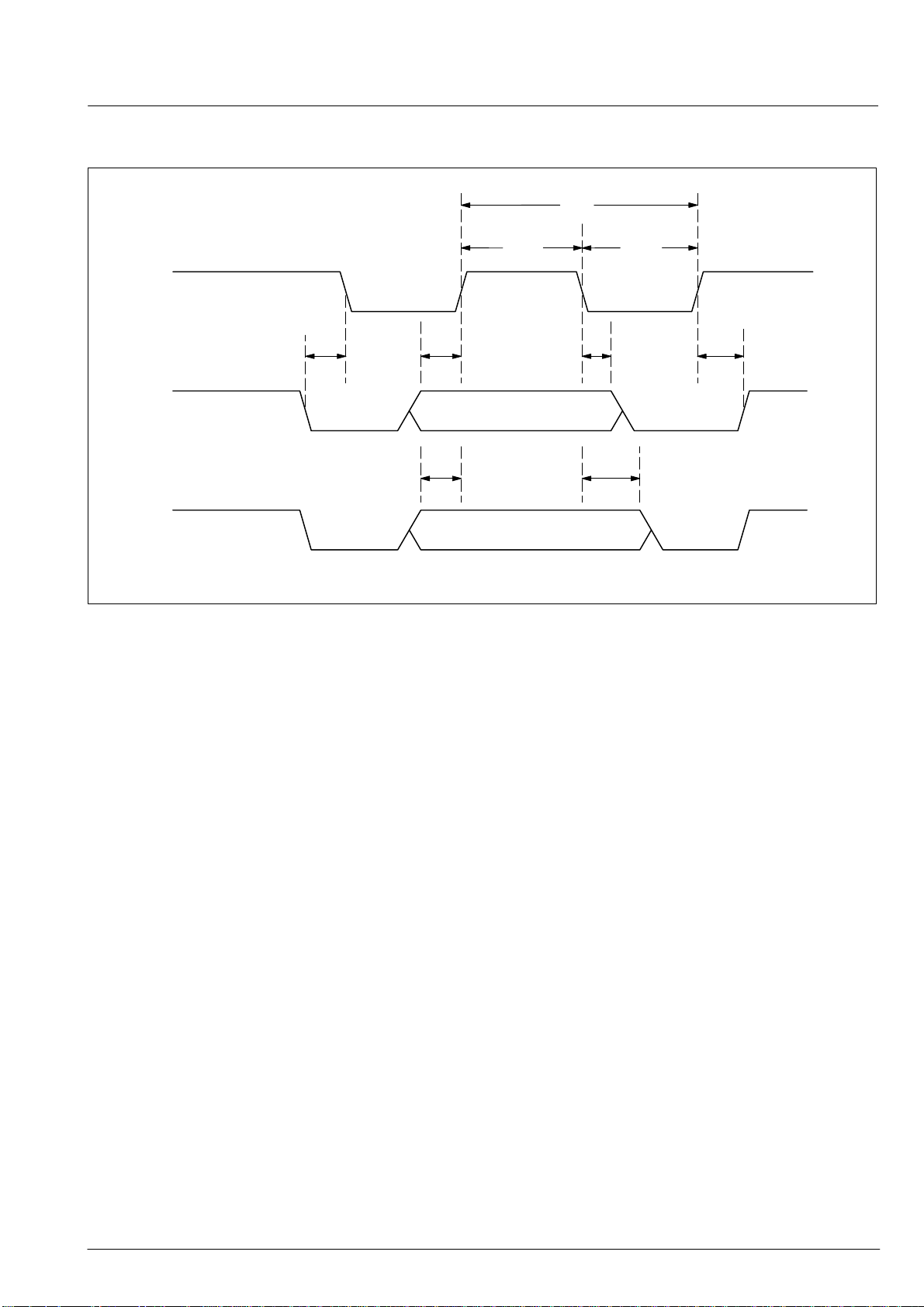
5.3. Control Bus Timing Diagram
VPX 3225D, VPX 3224DPRELIMINARY DATA SHEET
(Data: MSB first)
SCL
T
I2C1
SDA as input
SDA as output
Fig. 5–3: I2C bus timing diagram
T
I2C5
T
IMOL2
T
I2C4
F
IM
T
I2C3
T
I2C6
T
IMOL1
T
I2C2
61Micronas
Page 62
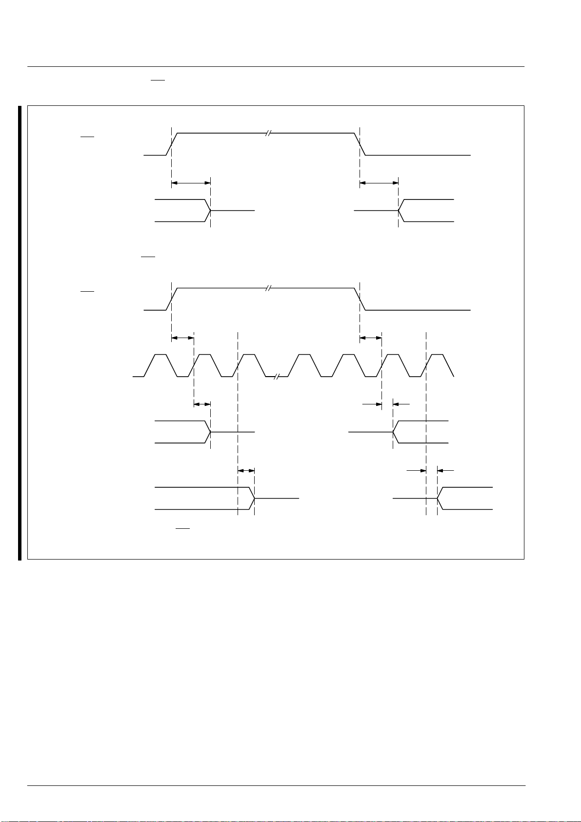
VPX 3225D, VPX 3224D
5.4. Output Enable by Pin OE
OE
PRELIMINARY DATA SHEET
t
OFF
Signals
A[7:0], B[7:0]
Synchronizing the OE signal with clock LLC:
2
controlled by I
C register ’OENA’ h’f2 bit[5] oeqdel = 1
OE
t
SU
t
OFF1
latoeq = 0
Signals
A[7:0], B[7:0]
t
ON1
t
ON
t
SU
latoeq = 1
Signals
A[7:0], B[7:0]
Fig. 5–4: Drive Control by OE input
t
OFF1
t
ON1
62 Micronas
Page 63
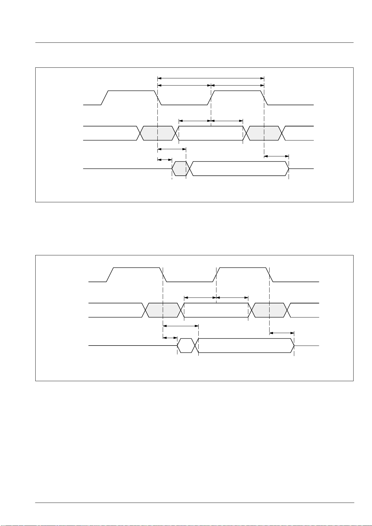
5.5. Timing of the Test Access Port TAP
TCK
F
L–TAP
F
CYCL
VPX 3225D, VPX 3224DPRELIMINARY DATA SHEET
F
H-TAP
t
S-TAP
t
H-TAP
TDI, TMS
t
D-TAP
t
ON-TAP
TDO
Fig. 5–5: Timing of Test Access Port TAP
5.6. Timing of all Pins connected to the Boundary-Scan-Register-Chain
TCK
t
S-PINS
t
H-PINS
t
OFF-TAP
Inputs
t
D-PINS
t
ON-PINS
Outputs
Fig. 5–6: Timing with respect to input and output signals
t
OFF-PINS
63Micronas
Page 64
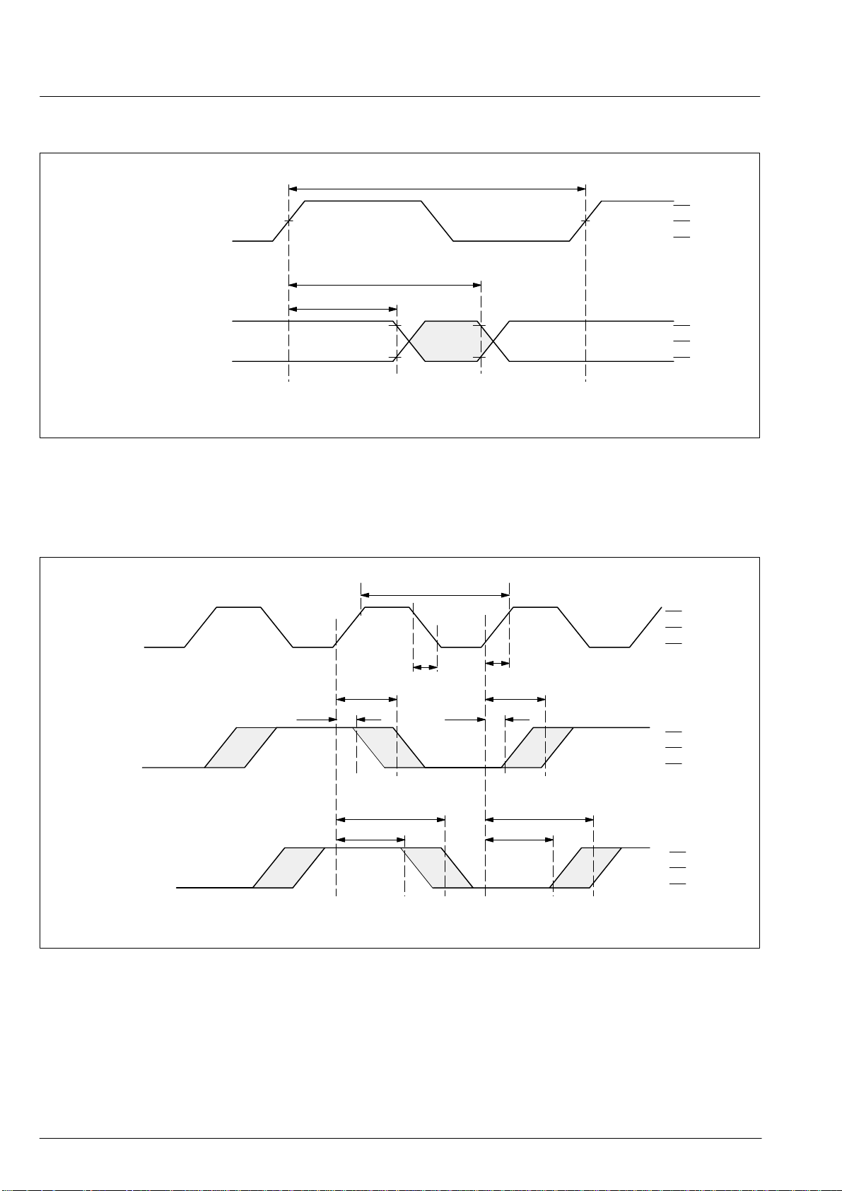
VPX 3225D, VPX 3224D
5.7. Timing Diagram of the Digital Video Interface
Clock Output LLC
t
OH
A[7:0], B[7:0]
HREF, VREF, FIELD, VACT
Fig. 5–7: Video output interface (detailed timing)
PRELIMINARY DATA SHEET
t
LLC
2.4 V
1.5 V
0.6 V
t
PD
2.4 V
1.5 V
0.6 V
5.7.1. Characteristics, Clock Signals
LLC
LLC2
PIXCLK
Fig. 5–8: Clocks: LLC, LLC2, PIXCLK (detailed timing)
t
HCLK1
t
DCLK1
t
HCLK2
t
DCLK2
t
LLC
2.4 V
1.5 V
t
t
FA
t
HCLK1
RA
t
DCLK1
t
HCLK2
t
DCLK2
0.6 V
2.4 V
1.5 V
0.6 V
2.4 V
1.5 V
0.6 V
64 Micronas
Page 65
VPX 3225D, VPX 3224DPRELIMINARY DATA SHEET
6. Control and Status Registers
The following tables give definitions for the VPX control
and status registers. The number of bits indicated for
The control register modes are
– w write-only register
– r read-only register
each register in the table is the number of bits implemented in the hardware, i.e. a 9-bit register must always
be accessed using two data bytes, but the 7 MSB will be
“0” on write operations and don’t care on read operations. Write registers that can be read back are indicated
– w/r write/read register
– d register is double latched
– v register is latched with vsync
in the mode column.
Default values are initialized at reset. The mnemonics
used in the Micronas VPX demo software are given in
the last column.
6.1. Overview
I2C-Registers
Address
Hex
h’00 8 r Manufacture ID Chip Ident. JEDEC
h’01
h’02
h’03 8 r JEDEC2 Chip Ident. JEDEC2
h’35 8 r FP status FP Interface FPSTA
h’36 16 w FP read FP Interface FPRD
h’37 16 w FP write FP Interface FPWR
h’38 16 w/r FP data FP Interface FPDAT
h’AA 8 w Low power mode, LLC mode Output llc
h’B3 8 r soft error counter Byte Slicer softerrcnt
h’B4 8 r sync status Sync Slicer sync_stat
h’B5 8 r hsync counter Sync Slicer sync_cnt
h’B6 8 r read filter coefficient Bit Slicer coeff_rd
h’B7 8 r read data slicer level Bit Slicer level_rd
h’B8
h’B9
h’BA
h’BB
h’BC
h’BD
h’C0 8 w soft slicer level Bit Slicer soft_slicer
h’C1
h’C2
h’C5 8 w filter coefficient Bit Slicer coeff
h’C6 8 w data slicer level Bit Slicer data_slicer
h’C7 8 w accumulator mode Bit Slicer accu
h’C8 8 w sync slicer level Sync Slicer sync_slicer
h’C9 8 w standard Byte Slicer standard
h’CE 8 w bit error tolerance Byte Slicer tolerance
h’CF 8 w byte count Byte Slicer byte_cnt
h’F2 8 w Output Enable Output oena
h’F8 8 w Pad Driver Strength – TTL Output Pads Type A Output driver_a
h’F9 8 w Pad Driver Strength – TTL Output Pads Type B Output driver_b
Number
of Bits
8
8
8
8
8
8
8
8
8
8
Mode Function Group Name
r 16-bit part number Chip Ident. PARTNUM
w
w
w
w
w
w
w
w
clock run-in and framing code don’t care mask high
clock run-in and framing code don’t care mask mid
clock run-in and framing code don’t care mask low
clock run-in and framing code reference high
clock run-in and framing code reference mid
clock run-in and framing code reference low
ttx bitslicer frequency LSB
ttx bitslicer frequency MSB
Byte Slicer mask
Byte Slicer reference
Bit Slicer ttx_freq
65Micronas
Page 66
VPX 3225D, VPX 3224D
PRELIMINARY DATA SHEET
FP-RAM
Address
Hex
h’12 12 r/w general purpose control Status gp_ctrl
h’13 12 r standard recognition status Status asr
h’15 12 r vertical field counter Status vcnt
h’20 12 w Standard select Stand. Sel. sdt
h’21 12 w Input select Stand. Sel. insel
h’22 12 w start point of active video Stand. Sel. sfif
h’23 12 w luma/chroma delay adjust Stand. Sel. ldly
h’30 12 w ACC reference level to adjust Cr, Cb levels on picture bus Color Proc. accref
h’31 12 r measured burst amplitude Status bampl
h’32 12 w ACC multiplier value for SECAM Db chroma comp. to adjust
h’33 12 w ACC multiplier value for SECAM Dr chroma comp. to adjust
h’39 12 w amplitude killer level Color Proc. kilvl
h’3A 12 w amplitude killer hysteresis Color Proc. kilhy
h’74 12 r measured sync amplitude value Status sampl
h’CB 12 r number of lines per field, P/S: 312, N: 262 Status nlpf
h’DC 12 w NTSC tint angle, $512 = $π/4 Color Proc. tint
h’F0 12 r software version number Status version
h’F7 12 w/r crystal oscillator line-locked mode, DVCO xlck
h’F8 12 w crystal oscillator center frequency adjust DVCO dvco
h’F9 12 r crystal oscillator center frequency adjustment value DVCO adjust
h’10F 12 r Delay of VACT relative to HREF during window 1 ReadTab1 vact_dly1
h’11F 12 r Delay of VACT relative to HREF during window 2 ReadTab2 vact_dly2
h’120 12 w V ertical Begin WinLoadTab1 vbegin1
h’121 12 w Vertical Lines In / Temporal Decimation / Field Select WinLoadTab1 vlinesin1
h’122 12 w Vertical Lines Out WinLoadTab1 vlinesout1
h’123 12 w Horizontal Begin WinLoadTab1 hbeg1
h’124 12 w Horizontal Length WinLoadTab1 hlen1
h’125 12 w Number of Pixels WinLoadTab1 npix1
h’126 12 w Selection for peaking / coring WinLoadTab1 peaking1
h’127 12 w Brightness WinLoadTab1 brightness1
h’128 12 w Contrast / Noise shaping / Clamping WinLoadTab1 contrast1
h’12A 12 w Vertical Begin WinLoadTab2 vbegin2
h’12B 12 w Vertical Lines In WinLoadTab2 vlinesin2
h’12C 12 w Vertical Lines Out WinLoadTab2 vlinesout2
h’12D 12 w Horizontal Begin WinLoadTab2 hbeg2
h’12E 12 w Horizontal Length WinLoadTab2 hlen2
h’12F 12 w Number of Pixels WinLoadTab2 npix2
h’130 12 w Selection for peaking / coring WinLoadTab2 peaking2
h’131 12 w Brightness WinLoadTab2 brightness2
Number
of Bits
Mode Function Group Name
C
on pict. bus
b
C
on pict. bus
r
Color Proc. accb
Color Proc. accr
66 Micronas
Page 67
VPX 3225D, VPX 3224DPRELIMINARY DATA SHEET
FP-RAM
Address
Hex
h’132 12 w Contrast WinLoadTab2 contrast2
h’134 12 w Start line even field VBI-window start_even
h’135 12 w End line even field VBI-window end_even
h’136 12 w Start line odd field VBI-window start_odd
h’137 12 w End line odd field VBI-window end_odd
h’138 12 w Control VBI-Window VBI-window vbicontrol
h’139 12 w Slicer Data Size VBI-window slsize
h’140 12 w r Register for control and latching ControlWord
h’141 12 r Internal status register, do not overwrite InfoWord
h’150 12 w Format Selection / Shuffler / PIXCLK-mode Formatter format_sel
h’151 12 w Start position of the programmable ‘video active’ HVREF pval_start
h’152 12 w End position of the programmable ‘video active’ HVREF pval_stop
h’153 12 w Length and polarity of HREF, VREF, FIELD HVREF refsig
h’154 12 w Output Multiplexer / Multi-purpose output Output Mux. outmux
h’157 12 w Number of frames to output within 3000 frames Temp. Decim. tdecframes
of Bits
NameGroupFunctionModeNumber
67Micronas
Page 68
VPX 3225D, VPX 3224D
6.1.1. Description of I2C Control and Status Registers
2
Table 6–1: I
C-Registers VPX Front-End
I2C-Registers VPX Front-End
PRELIMINARY DATA SHEET
Address
Hex
h’35 8 r FP status
h’36 16 w FP read
h’37 16 w FP write
h’38 16 w/r FP data
Number
of bits
Mode Function Default Name
bit [0] write request
bit [1] read request
bit [2] busy
bit [8:0] 9-bit FP read address
bit [11:9] reserved, set to zero
bit [8:0] 9-bit FP write address
bit [11:9] reserved, set to zero
bit [11:0] FP data register, reading/writing to this
FP Interface
register will autoincrement the FP read/
write address. Only 16 bit of data are
transferred per I
2
C telegram.
FPSTA
FPRD
FPWR
FPDAT
Table 6–2: I2C-Registers VPX Back-End
I2C-Registers VPX Back-End
Address
Hex
Number
of bits
Mode Function Default Name
Chip Identification
h’00 8 r Manufacture ID in accordance with
h’01
h’02
h’03 8 r JEDEC2 JEDEC2
8
8
r
r
JEDEC Solid State Products Engineering Council, Washington DC
Micronas Code EC
16 bit part number (01: LSBs, 02: MSBs)
VPX 3225D 7230
bit [0] : IFIELD ifield
bit [7:1] : reserved (must be treated don’t care)
hex
; VPX 3224D 7231
hex
hex
JEDEC
PARTNUM
partlow
parthigh
68 Micronas
Page 69
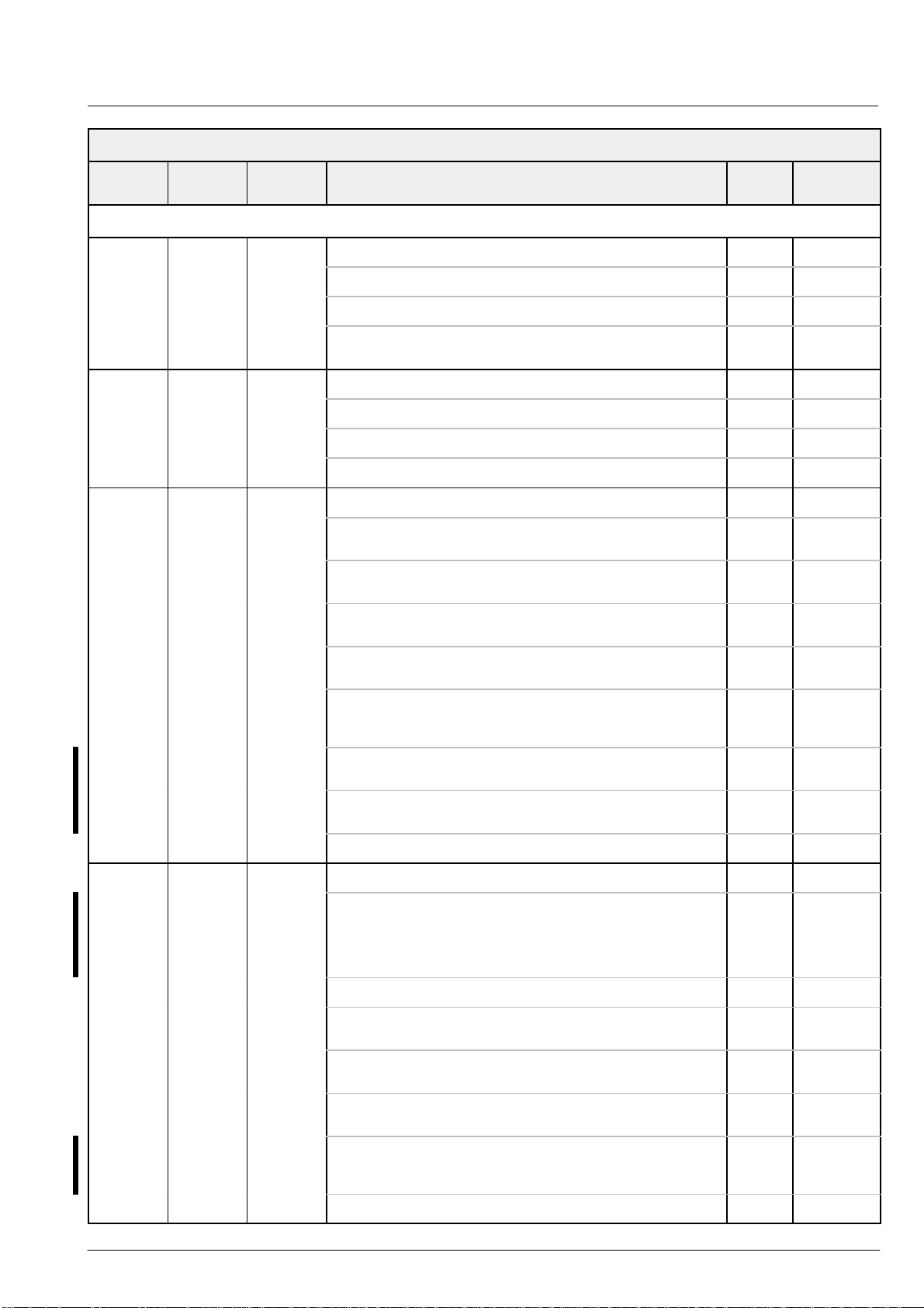
VPX 3225D, VPX 3224DPRELIMINARY DATA SHEET
I2C-Registers VPX Back-End
Address
Hex
of bits
NameDefaultFunctionModeNumber
Output
h’F8 8 w Pad Driver Strength – TTL Output Pads Typ A DRIVER_A
bit [2:0] : Driver strength of Port A[7:0] stra1
bit [5:3] : Driver strength of PIXCLK, LLC, and VACT stra2
bit [7:6] : additional PIXCLK driver strength
strength = bit [5:3] | {bit [7:6], 0}
h’F9 8 w Pad Driver Strength – TTL Output Pads Typ B DRIVER_B
bit [2:0] : Driver strength of Port B[7:0] strb1
bit [5:3] : Driver strength of HREF, VREF, FIELD, and LLC2 strb2
bit [7:6] : reserved (must be set to zero)
h’F2 8 w Output Enable OENA
direct bit [0] : 1 Enable Video Port A
0 Disable / High Impedance Mode
direct bit [1] : 1 Enable Video Port B
0 Disable / High Impedance Mode
direct bit [2] : 1 Enable Pixclk Output
0 Disable / High Impedance Mode
stra3
aen
ben
clken
direct bit [3] : 1 Enable HREF, VREF, FIELD, VACT, LLC, LLC2
0 Disable / High Impedance Mode
direct bit[4] 1 Enable LLC2 to TDO pin
(if JTAG interface is in Test-Logic-Reset State)
0 Disable LLC2
direct bit [5] : 1 no delay of OEQ input signal
0 1 LLC cycle delay of OEQ input signal (if bit [6] = 1)
direct bit [6] : 1 latch OEQ input signal with rising edge of LLC
0 don’t latch OEQ input signal
direct bit [7] : 1 disable OEQ pin function oeq_dis
h’AA 8 w Low power mode, LLC mode LLC
bit [1:0] : Low power mode
00 active mode, outputs enabled
01 outputs tri-stated; clock divided by 2, I2C full speed
10 outputs tri-stated; clock divided by 4, I2C full speed
11 outputs tri-stated; clock divided by 8, I2C < 100 kbit/s
bit [2] : I2C reset iresen
bit [3] : 1 connect LLC2 to TDO pin
0 connect bit[4] to TDO pin
bit [4] : if bit[3] then bit[4] defines LLC2 polarity
else bit[4] is connected to TDO pin
bit [5] : switch-off slicer
(if slowpow = 1 then all slicer registers are reset).
zen
llc2en
oeqdel
latoeq
lowpow
llc2
llc2_pol
slowpow
bit [6] : 1 use old llc timing with long hold time
0 use new llc timing with shorter hold time
(version D4 only)
bit [7] : reserved (must be set to zero)
oldllc
69Micronas
Page 70

VPX 3225D, VPX 3224D
Table 6–3: I2C-Registers VPX Slicer
PRELIMINARY DATA SHEET
I2C-Registers VPX Slicer
Address
Hex
h’C8 8 w sync slicer
h’B4 8 r sync status
h’B5 8 r hsync counter
h’C0 8 w soft slicer
h’C1
h’C2
Number
of bits
8
8
Mode Function Default Name
bit [6:0] : binary sync slicer level is compared with binary data
bit [7] : 0 vertical sync window enable
bit [5:0] : reserved (must be read don’t care)
bit [6] : 0 vert. window reset at line 624/524 (PAL/NTSC)
bit [7] : 0 field 2 reset at line 313/263 (PAL/NTSC)
bit [7:0] : number of detected horizontal sync pulses per frame / 4
bit [6:0] : binary soft slicer level is compared with ABS[data]
bit [7] : reserved (must be set to zero)
w
w
ttx bitslicer frequency LSB
ttx bitslicer frequency MSB
bit [10:0] : Freq = 2
bit [11] : 0 phase inc = Freq
bit [15:12] :reserved (must be set to zero)
(0 ≤ data ≤127)
1 vertical sync window disable
1 vert. retrace set at line 628/528 (PAL/NTSC)
1 field 1 set at line 624/524 (PAL/NTSC)
sync is detected within horizontal window of HPLL
counter is latched with vertical sync
the register can be read at any time
(–128 ≤data≤ +127)
1 phase inc = Freq*(1+1/8) before framing code
Sync Slicer
Bit Slicer
11
* bitfreq / 20.25MHz
= 702 for WST PAL
= 579 for WST NTSC or NABTS
= 506 for VPS or WSS
= 102 for CAPTION
= 627 for Antiope
= 183 for Time Code
phase inc = Freq*(1+1/16) after framing code
64
0
16
702
1
0
sync_slicer
sync_level
vsw
sync_stat
vwin
field
sync_cnt
soft_slicer
soft_level
ttx_freql
ttx_freqh
ttx_freq
ttx_phinc
h’C5 8 w filter coefficient
bit [5:0] : high pass filter coefficient in 2’s complement
100000 = not allowed
100001 = –31
000000 = 0
011111 = +31
bit [7:6] : reserved (must be set to zero)
h’C6 8 w data slicer
bit [7:0] : binary data slicer level is compared with ABS[data]
(–128 ≤ data ≤+127)
7
64
filter
coeff
data_slicer
data_level
70 Micronas
Page 71

I2C-Registers VPX Slicer
VPX 3225D, VPX 3224DPRELIMINARY DATA SHEET
Address
Hex
h’C7 8 w accumulator mode
h’B6 8 r read filter coefficient coeff_rd
h’B7 8 r read data slicer level level_rd
of bits
bit [0] : 0 no action
1 reset DC and AC and FLT accu (one shot)
bit [1] : 0 DC accu enable
1 DC accu disable
bit [2] : 0 AC and FLT accu enable
1 AC and FLT accu disable
(only for VPS and CAPTION and WSS line)
bit [3] : 0 soft error correction enable
1 soft error correction disable
bit [4] : 0 ac adaption disable
1 ac adaption enable
bit [5] : 0 flt adaption disable
1 flt adaption enable
bit [7:6] : reserved (must be set to zero)
0
0
1
0
1
1
NameDefaultFunctionModeNumber
accu
reset
dcen
acen
soften
acaden
fltaden
Byte Slicer
h’B3 8 r soft error counter
bit [7:0] : counts number of soft error corrected bytes
counter stops at 255
reset after read
h’C9 8 w standard
bit [0] : 0 TTX disable
1 TTX enable
bit [1] : 0 PAL mode
1 NTSC mode
bit [2] : 0 full field disable
1 full field enable
bit [3] : 0 VPS line 16 disable
1 VPS line 16 enable
bit [4] : 0 WSS line 23 disable
1 WSS line 23 enable
bit [5] : 0 CAPTION line 21 field 1 disable
1 CAPTION line 21 field 1 enable
bit [6] : 0 CAPTION line 21 field 2 disable
1 CAPTION line 21 field 2 enable
bit [7] : 0 horizontal quit signal enable
1 horizontal quit signal disable
1
0
0
1
1
0
0
0
soft_cnt
standard
ttx
ntsc
full
vps
wss
caption1
caption2
disquit
h’BD
h’BC
h’BB
h’BA
h’B9
h’B8
h’CE 8 w bit error tolerance
h’CF 8 w output mode
8
8
8
8
8
8
w
w
w
w
w
w
clock run-in and framing code reference low
clock run-in and framing code reference mid
clock run-in and framing code reference high
bit [23:0] : clock run-in and framing code reference
(LSB corresponds to first transmitted bit)
clock run-in and framing code don’t care mask low
clock run-in and framing code don’t care mask mid
clock run-in and framing code don’t care mask high
bit [23:0] : clock run-in and framing code don’t care mask
(LSB corresponds to first transmitted bit)
bit [1:0] : maximum number of bit errors in low mask
bit [3:2] : maximum number of bit errors in mid mask
bit [5:4] : maximum number of bit errors in high mask
bit [7:6] : reserved (must be set to zero)
bit [5:0] : number of data bytes per text line including framing code
bit [6] : 0 64 byte mode disable
1 64 byte mode enable
bit [7] : 0 data output only for text lines
1 data output for every video line
h’55
h’55
h’27
h’00
h’00
h’00
1
1
1
43
1
0
reference
mask
tolerance
out_mode
byte_cnt
fill64
dump
71Micronas
Page 72
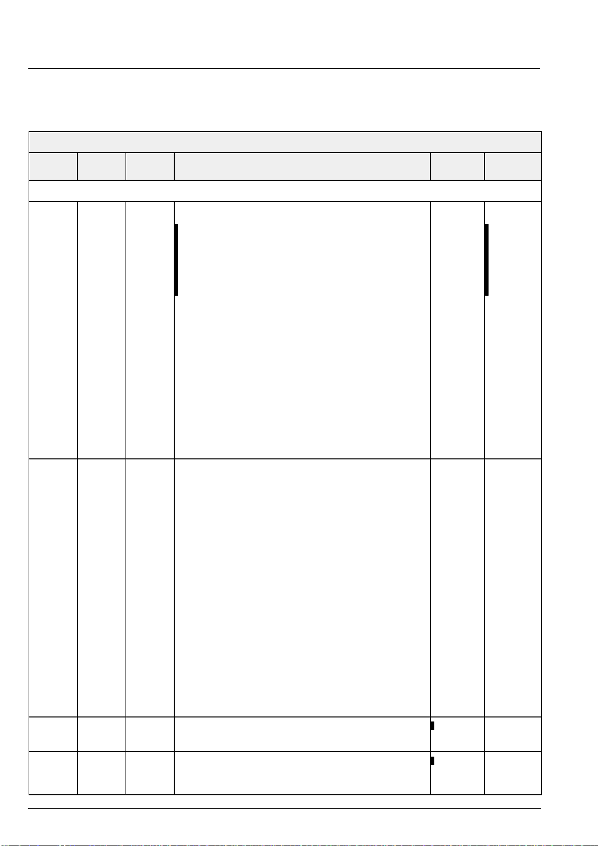
VPX 3225D, VPX 3224D
6.1.2. Description of FP Control and Status Registers
Table 6–4: FP-RAM VPX Front-End
FP-RAM VPX Front-End
PRELIMINARY DATA SHEET
Address
Hex
Number
of Bits
Mode Function Default Name
Standard Selection
h’20 12 w Standard select:
h’21 12 w Input select: Writing to this register will also initialize the standard.
bit [2:0] standard
0 PAL B,G,H,I (50 Hz) 4.433618
1 NTSC M (60 Hz) 3.579545
2 SECAM (50 Hz) 4.286
3 NTSC44 (60 Hz) 4.433618
4 PAL M (60 Hz) 3.575611
5 PAL N (50 Hz) 3.582056
6 PAL 60 (60 Hz) 4.433618
7 NTSC COMB (60 Hz) 3.579545
bit [3] 0/1 MOD standard modifier
PAL modified to simple PAL
NTSC modified to compensated NTSC
SECAM modified to monochrome 625
NTSCC modified to monochrome 525
bit [5:4] reserved; must be set to zero
bit [6] 0/1 S-VHS mode off/on
Option bits allow to suppress parts of the initialization:
bit [7] no hpll setup
bit [8] no vertical setup
bit [9] no acc setup
bit [10] reserved, set to zero
bit [11] status bit, write 0. After the FP has switched to a new
standard, this bit is set to 1 to indicate operation
complete.
0
sdt
pal
ntsc
secam
ntsc44
palm
paln
pal60
ntscc
sdtmod
svhs
sdtopt
insel
bit [1:0] luma selector
00 VIN3
01 VIN2
10 VIN1
11 reserved
bit [2] chroma selector
0/1 VIN1/CIN
bit [4:3] IF compensation
00 off
01 6 dB/Okt
10 12 dB/Okt
11 10 dB/MHz only for SECAM
bit [6:5] chroma bandwidth selector
00 narrow
01 normal
10 broad
11 wide
bit [7] 0/1 adaptive/fixed SECAM notch filter
bit [8] 0/1 enable luma lowpass filter
bit [10:9] hpll speed
00 no change
01 terrestrial
10 vcr
11 mixed
bit [11] status bit, write 0; This bit is set to 1 to indicate
operation complete.
h’22 12 w picture start position, This register sets the start point of active vid-
eo. This can be used e.g. for panning. The setting is updated when
’sdt’ register is updated
h’23 12 w luma/chroma delay adjust, The setting is updated when ’sdt’ register
is updated
bit [5:0] reserved, set to zero
bit [11:6] luma delay in clocks, allowed range is +1 ... –7
00
1
00
01
0 sfif
0 ldly
vis
cis
ifc
cbw
fntch
lowp
hpllmd
72 Micronas
Page 73
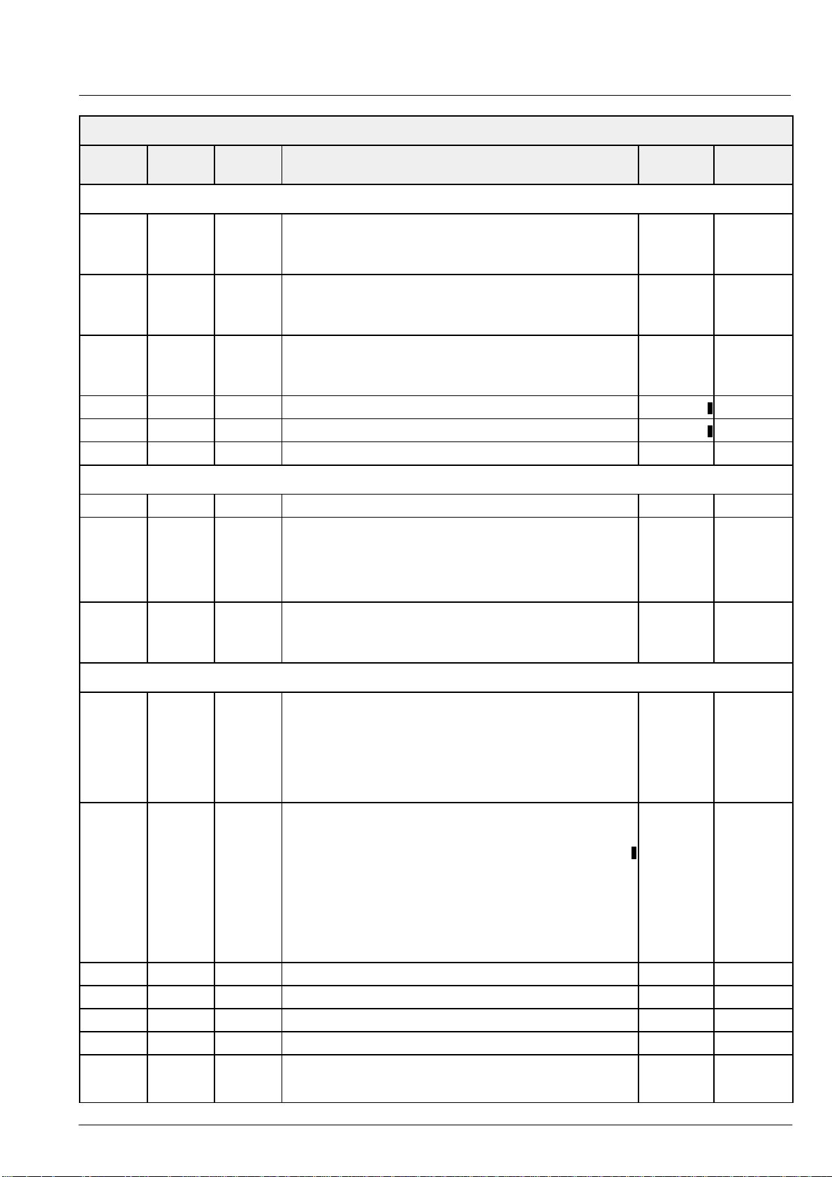
FP-RAM VPX Front-End
VPX 3225D, VPX 3224DPRELIMINARY DATA SHEET
Address
Hex
of Bits
NameDefaultFunctionModeNumber
Color Processing
h’30 12 w ACC reference level to adjust Cr, Cb levels on picture bus.
h’32 12 w ACC multiplier value for SECAM Db chroma component to adjust
h’33 12 w ACC multiplier value for SECAM Dr chroma component to adjust C
h’39 12 w amplitude killer level (0: killer disabled) 25 kilvl
h’3A 12 w amplitude killer hysteresis 5 kilhy
h’DC 12 w NTSC tint angle, $512 = $π/4 0 tint
A value of 0 disables the ACC, chroma gain can be adjusted via
ACCb / ACCr register. The setting is updated when ’sdt’ register is
updated.
Cb level on picture bus. The setting is updated when ’sdt’ register is
updated.
b [10:0] eeemmmmmmmm m * 2
level on picture bus. The setting is updated when ’sdt’ register is
updated.
b [10:0] eeemmmmmmmm m * 2
–e
–e
P/N: 2070
S: 0
S: 1155 accb
S: 1496 accr
r
accref
DVCO
h’F8 12 w crystal oscillator center frequency adjust, –2048 ... 2047 –720 dvco
h’F9 12 r crystal oscillator center frequency adjustment value for line-locked
mode, true adjust value is DVCO – ADJUST.
For factory crystal alignment, using standard video signal:
set DVCO = 0, set lock mode, read crystal offset from ADJUST
register and use negative value for initial center frequency adjustment via DVCO.
h’F7 12 w/r crystal oscillator line-locked mode, lock command/status
write: 100 enable lock
0 disable lock
read: 4095/0 locked/unlocked
0 xlck
adjust
FP Status Register
h’12 12 w/r general purpose control bits
h’13 12 r automatic standard recognition status
h’CB 12 r number of lines per field, P/S: 312, N: 262 nlpf
h’15 12 w/r vertical field counter , incremented per field vcnt
h’74 12 r measured sync amplitude value, nominal: 768 sampl
h’31 12 r measured burst amplitude bampl
h’F0 12 r software version number
bit [2:0] reserved, do not change
bit [3] vertical standard force
bit [8:4] reserved, do not change
bit [9] disable flywheel interlace
bit [11:10] reserved, do not change
to enable vertical free run mode set vfrc=1 and dflw=0
bit [0] 1 vertical lock
bit [1] 1 horizontally locked
bit [2] 1 no signal detected
bit [3] 1 color amplitude killer active
bit [4] 1 disable amplitude killer
bit [5] 1 color ident killer active
bit [6] 1 disable ident killer
bit [7] 1 interlace detected
bit [8] 1 no vertical sync detection
bit [9] 1 spurious vertical sync detection
bit [11:10] reserved
bit [7:0] internal software revision number
bit [11:8] software release
0
1
x
gp_ctrl
vfrc
dflw
asr
73Micronas
Page 74

VPX 3225D, VPX 3224D
PRELIMINARY DATA SHEET
FP-RAM VPX Front-End
Address
Hex
of Bits
NameDefaultFunctionModeNumber
Macrovision Detection (version D4 only)
h’170 12 r Status of macrovision detection mcv_status
bit [0]: AGC pulse detected
bit [1]: pseudo sync detected
h’171 12 w first line of macrovision detection window 6 mcv_start
h’172 12 w last line of macrovision detection window 15 mcv_stop
74 Micronas
Page 75
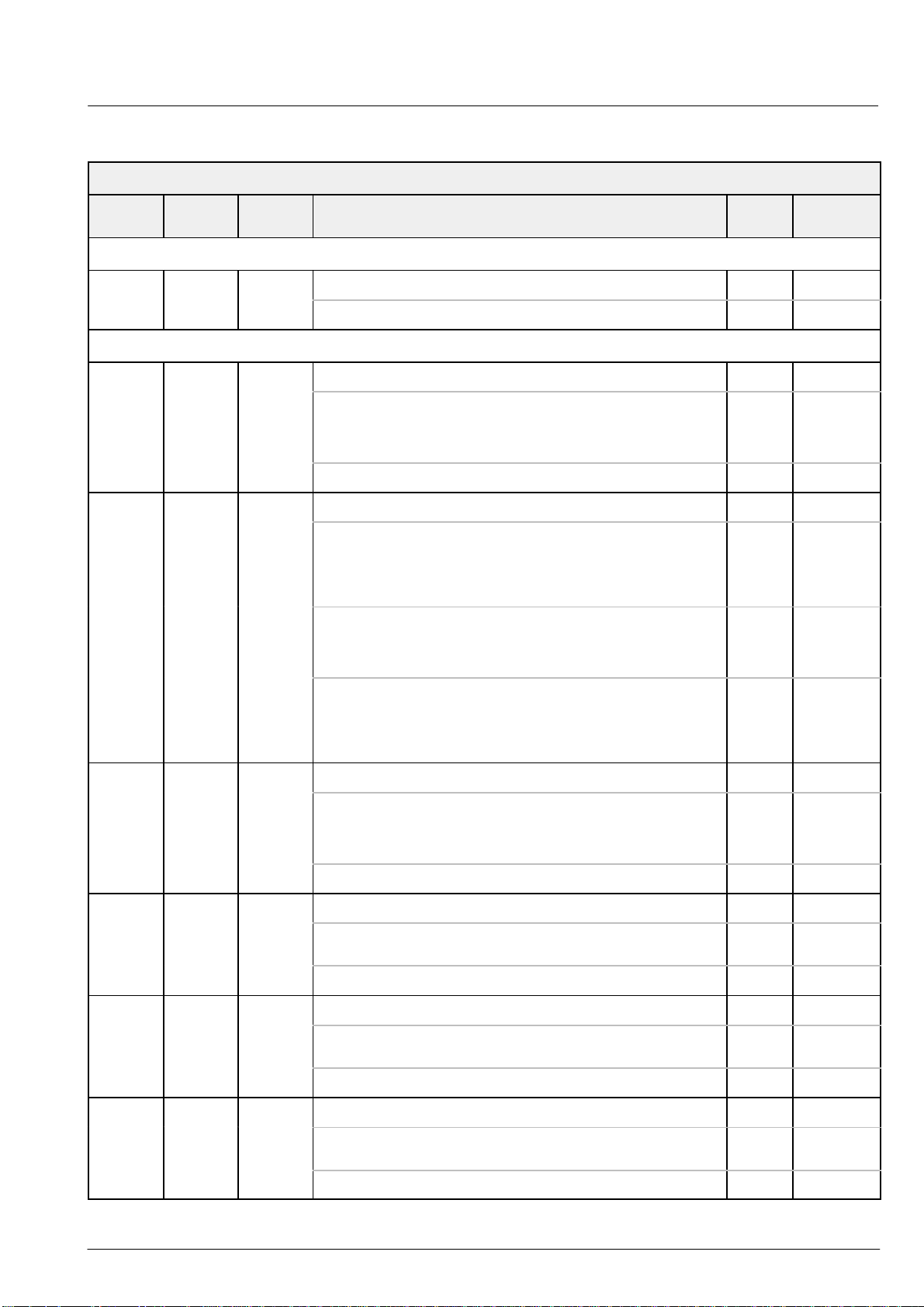
Table 6–5: FP-RAM VPX Back-End
VPX 3225D, VPX 3224DPRELIMINARY DATA SHEET
FP-RAM VPX Back-End
Address
Hex
Number
of Bits
Mode Function Default Name
Read Table for Window #1
h’10f 12 r Position of VACT
bit [11:1]: Delay of VACT relative to the trailing edge of HREF vact_delay1
Load Table for Window #1 (WinLoadTab1)
h’120 12 w Vertical Begin 12
bit [8:0]: Vertical Begin (first active video line within a field)
bit [11:9]: reserved (must be set to zero)
h’121 12 w Vertical Lines In 0
bit [8:0]: Number of input lines
bit [9]: enable temporal decimation (0: off, 1: on)
min. line number for 625/50 standards: 7
min. line number for 525/60 standards: 10
max. line number: determined by current TV line standard
determines the range between the first and the last active
video line within a field; vbeg + vlinei should not exceed the
max. number of lines determined by the current line
standard (exceeding values will be corrected automatically)
with temporal decimation enabled, only the number of frames
selected in register h’157 (tdecframes) will be output within
an interval of 3000 frames
vbeg1
vlinei1
tdec1
bit [11:10]: field disable flags
11 Window disabled
10 Window enabled in ODD fields only
01 Window enabled in EVEN fields only
00 Window enabled in both fields
h’122 12 w Vertical Lines Out 0
bit [8:0]: Number of output lines
vlineout cannot be greater than vlinein (no interpolation);
for vlineout < vlinein vertical compression via line dropping
is applied
bit [11:9]: reserved (must be set to zero)
h’123 12 w Horizontal Begin 0
bit [10:0]: Horizontal start of window after scaling (relative to npix)
hbeg > 0 enables cropping on the left side of the window
bit [11]: reserved (must be set to zero)
h’124 12 w Horizontal Length 704
bit [10:0]: Horizontal length of window after scaling (relative to npix)
hbeg + hlen cannot exceed npix
bit [11]: reserved (must be set to zero)
h’125 12 w Number of Pixels 704
bit [10:0]: Number of active pixels for the full active line (after scaling)
npix must be an even value within the range 32...864
vlineo1
hbeg1
hlen1
npix1
bit [11]: reserved (must be set to zero)
75Micronas
Page 76

VPX 3225D, VPX 3224D
PRELIMINARY DATA SHEET
FP-RAM VPX Back-End
Address
Hex
h’126 12 w Selection for peaking/coring 0 peaking1
of Bits
bit [1:0]: coring
subtracts LSBs of the higher frequency part of the video
signal
00: subtract 0 LSBs
01: subtract 1/2 LSB
10: subtract 1 LSB
11: subtract 2 LSBs
bit [4:2]: peaking
an implemented peaking filter supports sharpness control
with up to eight steps:
000:no peaking
001:low peaking
111: high peaking
bit [5]: Bypass Lowpass
bit [6]: Bypass Skewfilter
bit [7]: Bypass Skewfilter VACT
bit [8]: Swapping of Chroma values
0 Cb-Pixels first
1 Cr-Pixels first
bit [11:9]: reserved (must be set to zero)
NameDefaultFunctionModeNumber
h’127 12 w Brightness 0
bit [7:0]: Brightness Level
offset value added to the video samples
brightness can be selected in 256 steps within the range
–127...128 (binary offset format):
0: –127
255:128
bit [11:8]: reserved (must be set to zero)
h’128 12 w Contrast 32 contrast1
bit [5:0]: Contrast Level
linear scale factor for luminance (default = 1.0)
[5] integer part
[4:0]fractional part
bit [7:6]: Noise Shaping
Control for 10-bit to 8-bit conversion (default: rounding)
00: 9-bit to 8-bit via 1-bit rounding
01: 9-bit to 8-bit via truncation
10: 9-bit to 8-bit via 1-bit accumulation
11: 10-bit to 8-bit via 2-bit accumulation
bit [8]: Contrast Brightness: Clamping Level
0 clamping level = 32,
1 clamping level = 16
(should normally be set to 1)
bit [9]: Bypass Brightness Adder bribyp1
brightness1
contr1
noise1
clamp1
bit [10]: Bypass Contrast Multiplier conbyp1
bit [11]: reserved (must be set to zero)
76 Micronas
Page 77
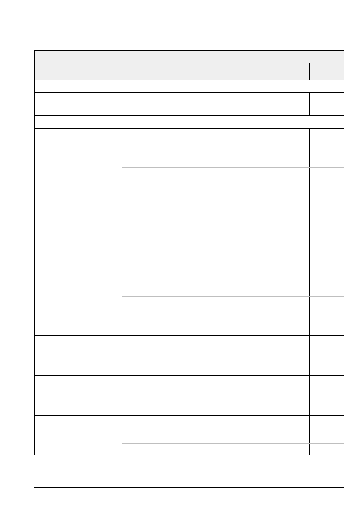
FP-RAM VPX Back-End
VPX 3225D, VPX 3224DPRELIMINARY DATA SHEET
Address
Hex
of Bits
Read Table for Window #2
h’11f 12 r Position of VACT
bit [11:1]: Delay of VACT relative to the trailing edge of HREF vact_delay2
Load Table for Window #2 (WinLoadTab2)
h’12A 12 w Vertical Begin 17
bit [8:0]: Vertical Begin (first active video line within a field)
bit [11:9]: reserved (must be set to zero)
h’12B 12 w Vertical Lines In 500
bit [8:0]: Number of input lines
bit [9]: enable temporal decimation (0: off, 1: on)
min. line number for 625/50 standards: 7
min. line number for 525/60 standards: 10
max. line number: determined by current TV line standard
determines the range between the first and the last active
video line within a field; vbeg + vlinei should not exceed the
max. number of lines determined by the current line
standard (exceeding values will be corrected automatically)
with temporal decimation enabled, only the number of
frames selected in register h’157 (tdecframes) will be output
within an interval of 3000 frames
NameDefaultFunctionModeNumber
vbeg2
vlinei2
tdec2
bit [11:10]: field disable flags
11: Window disabled
10: Window enabled in ODD fields only
01: Window enabled in EVEN fields only
00: Window enabled in both fields
h’12C 12 w Vertical Lines Out 240
bit [8:0]: Number of output lines
vlineout cannot be greater than vlinein (no interpolation);
for vlineout < vlinein vertical compression via line dropping
is applied
bit [11:9]: reserved (must be set to zero)
h’12D 12 w Horizontal Begin 0
bit [10:0]: Horizontal start of window after scaling (relative to npix)
hbeg > 0 enables cropping on the left side of the window
bit [11]: reserved (must be set to zero)
h’12E 12 w Horizontal Length 640
bit [10:0]: Horizontal length of window after scaling (relative to npix)
hbeg + hlen can not exceed npix
bit [11]: reserved (must be set to zero)
h’12F 12 w Number of Pixels 640
bit [10:0]: Number of active pixels for the full active line (after scaling)
npix must be an even value within the range 32...864
vlineo2
hbeg2
hlen2
npix2
bit [11]: reserved (must be set to zero)
77Micronas
Page 78

VPX 3225D, VPX 3224D
PRELIMINARY DATA SHEET
FP-RAM VPX Back-End
Address
Hex
h’130 12 w Selection for peaking/coring 0 peaking2
of Bits
bit [1:0]: coring
subtracts LSBs of the higher frequency part of the video
signal
00: subtract 0 LSBs
01: subtract 1/2 LSB
10: subtract 1 LSB
11: subtract 2 LSBs
bit [4:2]: peaking
an implemented peaking filter supports sharpness control
with up to eight steps:
000:no peaking
001:low peaking
111: high peaking
bit [5]: Bypass Lowpass
bit [6]: Bypass Skewfilter
bit [7]: Bypass Skewfilter VACT
bit [8]: Swapping of Chroma values
0 Cb-Pixels first
1 Cr-Pixels first
bit [11:9]: reserved (must be set to zero)
NameDefaultFunctionModeNumber
h’131 12 w Brightness 0
bit [7:0]: Brightness Level
offset value added to the video samples
brightness can be selected in 256 steps within the range
–127...128 (binary offset format):
0: –127
255:128
bit [11:8]: reserved (must be set to zero)
h’132 12 w Contrast 32 contrast2
bit [5:0]: Contrast Level
linear scale factor for luminance (default = 1.0)
[5] integer part
[4:0]fractional part
bit [7:6]: Noise Shaping
Control for 10-bit to 8-bit conversion (default: rounding)
00: 9-bit to 8-bit via 1-bit rounding
01: 9-bit to 8-bit via truncation
10: 9-bit to 8-bit via 1-bit accumulation
11: 10-bit to 8-bit via 2-bit accumulation
bit [8]: Contrast Brightness: Clamping Level
0 clamping level = 32,
1 clamping level = 16
(should normally be set to 1)
bit [9]: Bypass Brightness Adder bribyp1
brightness2
contr1
noise1
clamp1
bit [10]: Bypass Contrast Multiplier conbyp1
bit [11]: reserved (must be set to zero)
78 Micronas
Page 79
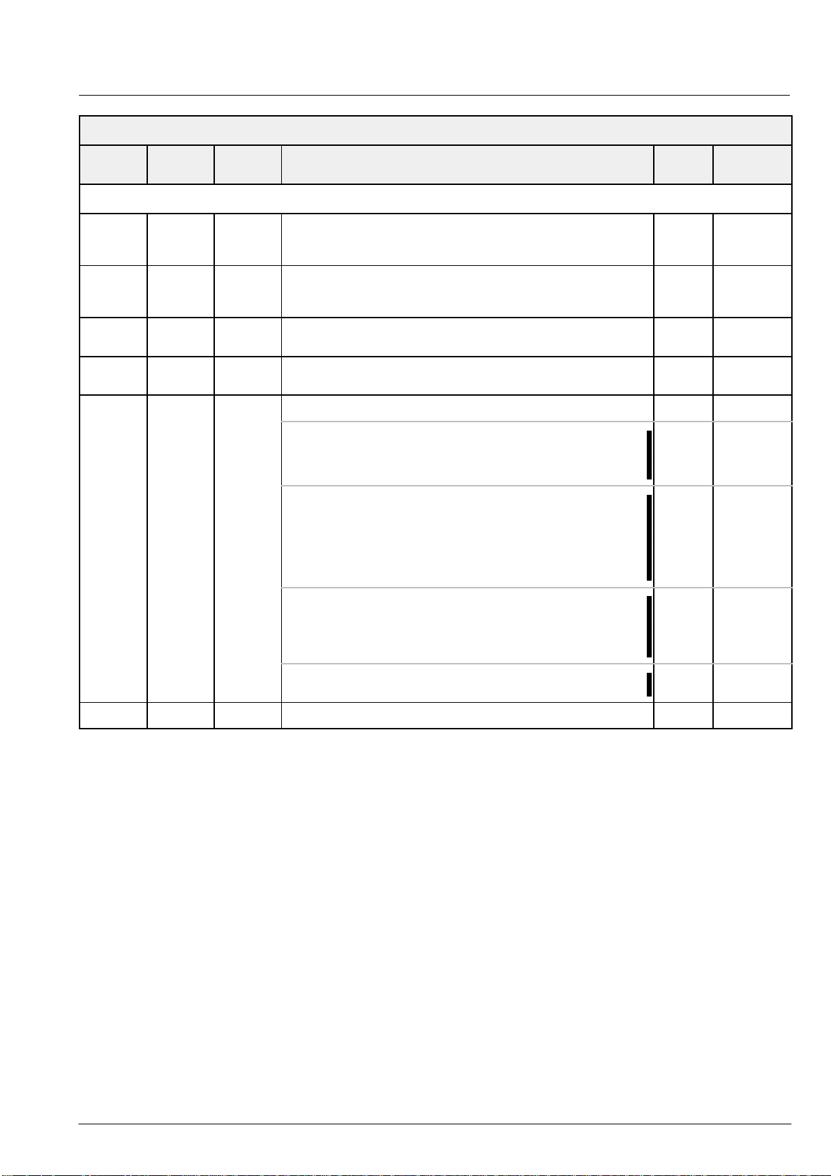
FP-RAM VPX Back-End
VPX 3225D, VPX 3224DPRELIMINARY DATA SHEET
Address
Hex
of Bits
NameDefaultFunctionModeNumber
Load Table for VBI-Window
h’134 12 w Start line even field
determines the first line of the VBI-window within even fields
(note that lines are counted relative to the whole frame!)
h’135 12 w End line even field
determines the last line of the VBI-window within even fields
(note that lines are counted relative to the whole frame!)
h’136 12 w Start line odd field
determines the first line of the VBI-window within odd fields
h’137 12 w End line odd field
determines the last line of the VBI-window within odd fields
h’138 12 w Control VBI-Window 0 vbicontrol
bit [0]: VBI-window enable
the selected VBI-window is activated only if this flag is set
0: disable
1: enable
bit [1]: VBI mode
two modes for the output of VBI-data are supported
0: raw data
1140 samples of the video input are given directly
to the output
1: sliced data
sliced teletext data (in a package of 64 bytes)
272 start_even
283 end_even
10 start_odd
21 end_odd
vbien
vbimode
bit [2]: vertical identification
the valid VBI-lines defined by the VBI-window can either be
marked as active or as blanked lines
0: active lines during VBI-window (VACT enabled)
1: blanked lines during VBI-window (VACT suppressed)
bit [11]: update the settings for the VBI-window
(settings will only be updated if this latch flag is set!)
h’139 12 w Slicer Data Size (0 corresponds to default value 64) 0 slsize
vbiident
vbilatch
79Micronas
Page 80
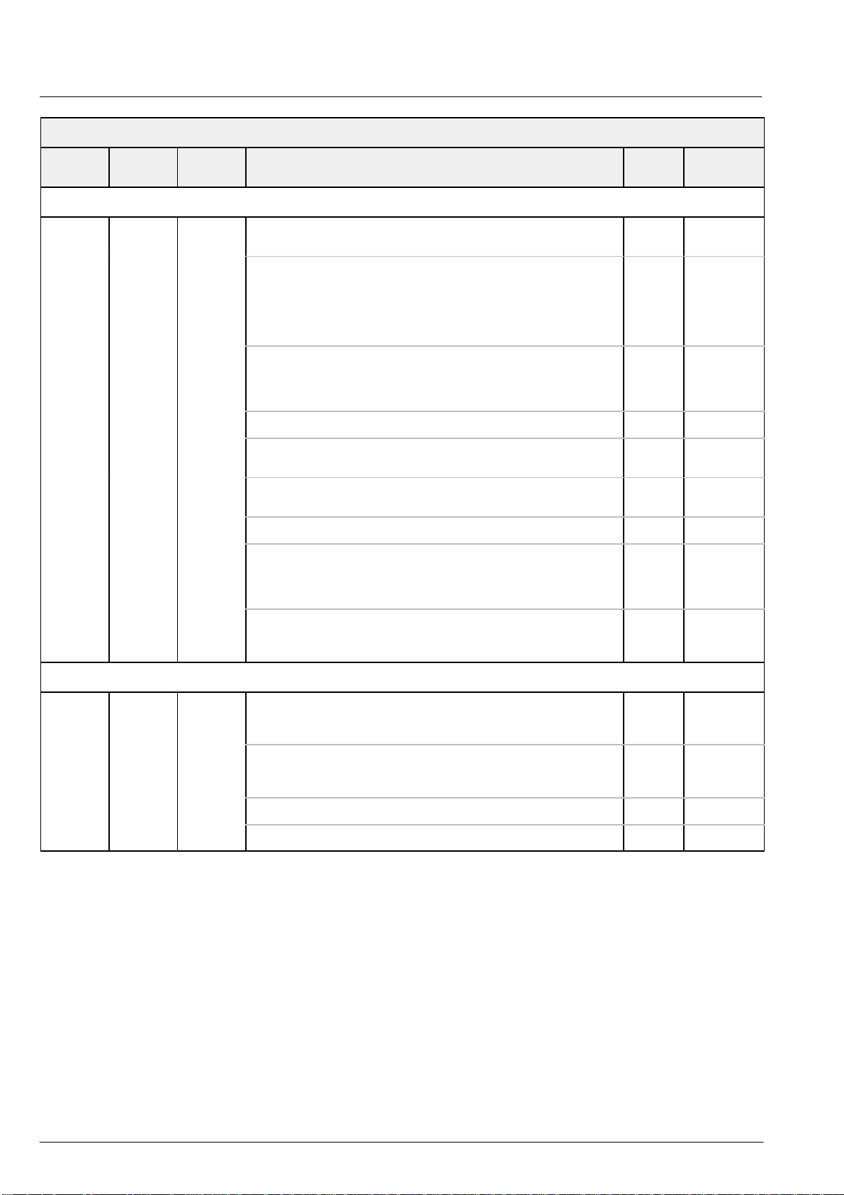
VPX 3225D, VPX 3224D
PRELIMINARY DATA SHEET
FP-RAM VPX Back-End
Address
Hex
of Bits
NameDefaultFunctionModeNumber
Control Word
h’140 12 w r Register for control and latching Control
w bit [1:0]: Sync timing mode
00 Open mode
horizontal and vertical sync are tracking the input
signal
10 Scan mode
horizontal and vertical sync are free running
w bit [2]: Mode for VACT reference signal
0 length of VACT corresponds to the size of the current
window
1 programmable length of VACT (for the whole field!)
w bit [4:3]: reserved (must be set to zero) 0
w bit [5]: Latch Window #1
1 latch (reset automatically)
w bit [6]: Latch Window #2
1 latch (reset automatically)
bit [9]: reserved (must be set to zero) 0
bit [10]: Latch value for temporal decimation
The number of frames for the temporal decimation is
updated only if this flag is set
1 latch (reset automatically)
0 settm
0 vactmode
1 latwin1
1 latwin2
1 lattdec
Word
w bit [11]: Latch Timing Modes
Selection of the timing mode is updated only if this flag is set
1 latch (reset automatically)
Info Word
h’141 12 r Internal status register, do not overwrite
This register can be used to query the current internal state due to the
settings in the control word.
bit [2]: Mode for VACT reference signal
0 current window size
1 programmable size
bit [4:3]: reserved
bit [11:8]: reserved
1 lattm
InfoWord
actvact
80 Micronas
Page 81
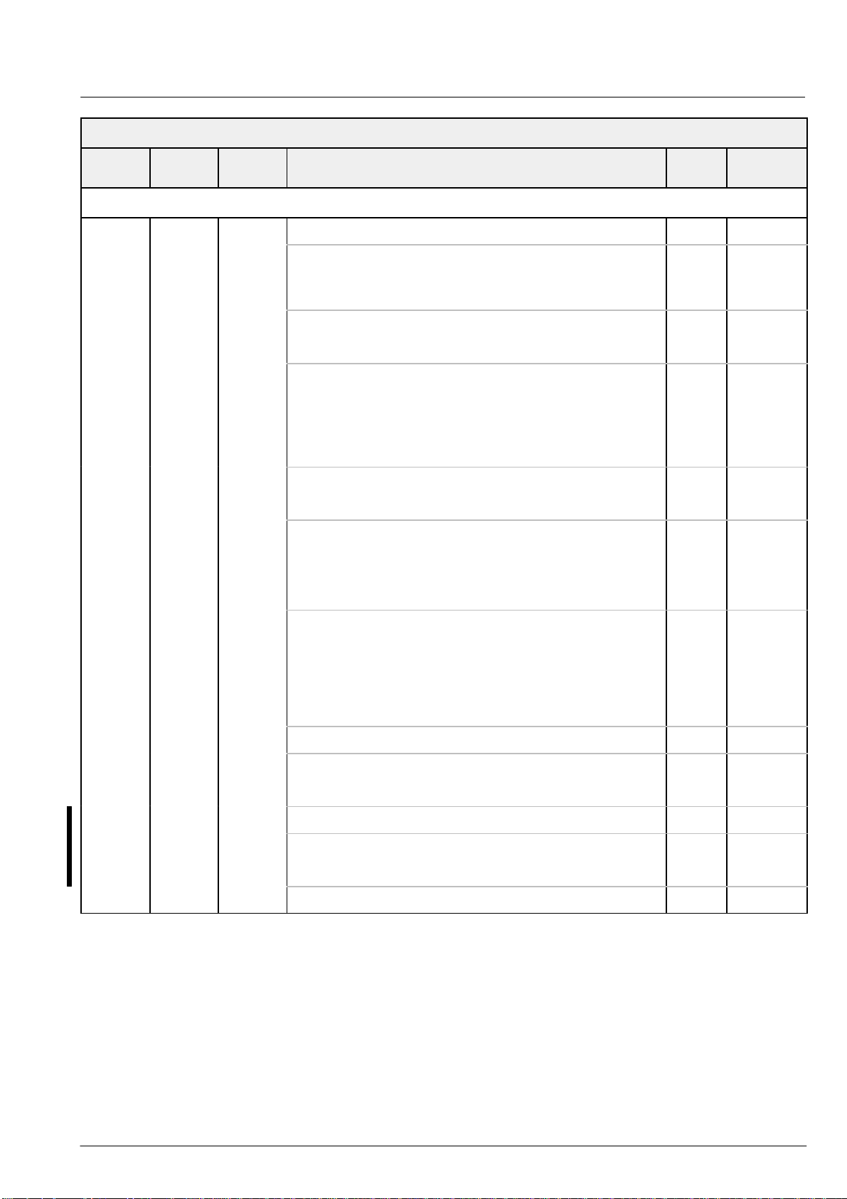
FP-RAM VPX Back-End
VPX 3225D, VPX 3224DPRELIMINARY DATA SHEET
Address
Hex
of Bits
NameDefaultFunctionModeNumber
Formatter
h’150 12 w Format Selection format_sel
bit [1:0]: Format Selector
00: YUV 4:2:2, ITU-R601
01: YUV 4:2:2, ITU-R656
10: YUV 4:2:2, BStream
bit [2]: Shuffler
0 Port A = Y, Port B = UV
1 Port A = UV, Port B = Y
bit [3]: Format of VBI-data (in ITU-R656 mode only!)
Two possibilities are supported to disable the protected
values 0 and 255:
0 limitation
1 7-bit resolution + odd parity LSB
Note that this selection is applied for lines within the VBIwindow only!
bit [4]: Transmission of VBI-data (in ITU-R656 mode only)
0 transmit as normal video data
1 transmit as ancillary data (with ANC-header)
bit [5]: PIXCLK selection
Setting this bit activates the half-clock mode, in which
PIXCLK is divided by 2 in order to spread the video data
stream
0 full PIXCLK (normal operation)
1 PIXCLK divided by 2
0 format
0 shuf
0 range
1 ancillary
0 halfclk
bit [6]: Disable splitting of text data bytes
During normal operation, sliced teletext bytes are splitted
into 2 nibbles and multiplexed to the luminance and
chrominance part. Setting this bit will disable this splitting.
Sliced teletext data will be output directly on the luminance
path. Note that the limitation of luminance data has to be
disabled with bit [8]. The values 0 and 255 will no longer be
protected in the luminance path!
bit [7]: reserved (must be set to zero) 0
bit [8]: Disable limitation of luminance data (see bit [6])
0 enabled
1 disabled
bit [9]: Suppress ITU–R656 headers for blank lines 0 hsup
bit [10]: Change of ITU–R656 header flags
0 change header flags in SA V
1 change header flags in EA V
bit [11]: reserved (must be set to zero) 0
0 splitdis
0 dislim
0 flagdel
81Micronas
Page 82

VPX 3225D, VPX 3224D
PRELIMINARY DATA SHEET
FP-RAM VPX Back-End
Address
Hex
of Bits
HVREF
h’151 12 w Start position of the programmable ‘video active’
h’152 12 w End position of the programmable ‘video active’
h’153 12 w HREF and VREF control
The start position has to be an even value and is given relative to the
trailing edge of HREF. Programmable VACT is activated with bit [2] of
the control word (h’140)!
bit [10:0]: start of VACT reference signal
The end position has to be an even value and is given relative to the
trailing edge of HREF.
bit [10:0]: end of VACT reference signal
determines length and polarity of the timing reference signals
bit [0]: Odd/Even polarity
0 odd high
1 even high
bit [1]: HREF Polarity
0 active high
1 active low
bit [2]: VREF Polarity
0 active high
1 active low
NameDefaultFunctionModeNumber
40 pval_
start
720 pval_stop
refsig
0 oepol
0 hpol
0 vpol
bit [5:3]: VREF pulse width, binary value + 2
000:pulse width = 2
111: pulse width = 9
bit [6]: 1 disables field as output
setting this bit will force the ‘field’ pin to the high impedance
state
0 vlen
0 disfield
Output Multiplexer
h’154 12 w Output Multiplexer 0 outmux
bit [7:0]: Multi-purpose bits on Port B
determines the state of Port B when used as programmable
output
bit [8]: activate multi-purpose bits on Port B
note that double clock mode has to be selected for this
option!
bit [9]: Port Mode
0 parallel_out, ‘single clock’, Port A & B = FO[15:0];
1 ‘double clock’
Port A = FO[15:8] / FO[7:0],
Port B = programmable output/not used;
bit [10]: switch ‘VBI active’ qualifier
0 connect ‘VBI active’ to VACT pin
1 connect ‘VBI active’ to TDO pin
bit [11]: reserved (must be set to zero)
bmp
bmpon
double
vbiact
Temporal Decimation
h’157 12 w Number of frames to output within 3000 frames
This value will be activated only if the corresponding latch flag is set
(control word h’140, bit [10] ).
3000 tdecframes
82 Micronas
Page 83
VPX 3225D, VPX 3224DPRELIMINARY DATA SHEET
7. Application Notes
7.1. Differences between VPX 3220A and VPX 322xD
The following items indicate the differences between the
VPX 322xD and the VPX 3220A:
Internal
– The control registers (I
2
C and FP-RAM) contain signif-
icant changes.
– VPX 322xD incorporates a text slicer. Furthermore,
raw ADC data is supported (sampling frequency of
20.25 MHz/8 bit, output data rate 13.5 MHz/16 bit).
– VPX 322xD does not support RGB and compressed
video data output formats. The VPX 322xD supports
ITU-R601 and ITU-R656.
– The VPX 322xD does not provide an asynchronous
output mode, PIXCLK functions as an output only . The
VPX 322xD supports half-clock data rate (6.75 MHz).
– The VPX 322xD does not provide a video data rate of
20.25 MHz at the output interface.
– The VPX 322xD has an implemented low power
mode.
7.2. Impact to Signal to Noise Ratio
Fig. 7–1 shows the impact of the variation of the power
supply with respect to the SNR of the ADCs. The noise
due to the digital output interface leads to an impact of
the analog performance of the analog ADCs. Application
engineers should minimize load capacitances and driver
strength of the output signals.
45
44
43
42
41
SNR [dB]
40
39
38
2.5 3.0 3.5 4.0 4.5 5.0 5.5 6.0
PVDD [V]
Fig. 7–1: Dependency between SNR and
Power Supply
Note: Both ADCs are working and routed to A[7:0], and
B[7:0]. All interfaces are working with maximum driver
strength bandwidth measurement is performed up to 5
MHz.
External
– Power-up Default Selection
Selection VPX 3220A VPX 322xD
I2C device
PREF OE
address
wake-up default
PIXCLK FIELD
Pads tristate/
active
– The VPX 322xD does not use the internal I2C bus for
power-up initialization. Resultingly, the I
2
C interface
will not be locked during that period.
– The VPX 322xD supports an 8-bit programmable out-
put port if the device uses only A[7:0] for video data
output.
– The VPX 322xD provides a HREF signal with a fixed
low period, whereas the width of the high period will
vary while the video input signal varies.
7.3. Control Interface
7.3.1. Symbols
< Start Condition
> Stop Condition
aa (Sub-)Address Byte
dd Data Byte
7.3.2. Write Data into I
<86 f2 dd> write to register OENA
2
C Register
7.3.3. Read Data from I2C Register
<86 00 <87 dd> read Manufacture ID
7.3.4. Write Data into FP Register
<86 35 <87 dd> poll busy bit[2] until it is cleared
<86 37 aa aa> write FP register write address
<86 35 <87 dd> poll busy bit[2] until it is cleared
<86 38 dd dd> write data into FP register
7.3.5. Read Data from FP Register
<86 35 <87 dd> poll busy bit[2] until it is cleared
<86 36 aa aa> write FP register read address
<86 35 <87 dd> poll busy bit[2] until it is cleared
<86 38 <87 dd dd> read data from FP register
83Micronas
Page 84

VPX 3225D, VPX 3224D
7.3.6. Sample Control Code
A Windows API function set is provided for controlling
the VPX. This API is independent of the actual used version of the VPX. It is recommended to control the VPX
via this API, which allows flexible switching between different VPX family members. The API is available on request. The following code demonstrates the usage of
the API to initialize the VPX.
#include <vpx.h> // VPXAPI support header
VPXInit(); // initializes the VPX from an INI file
VPXSetVideoSource(VPX_VIN1, VPX_COMPOSITE);
VPXSetVideoWindow(VPX_VIDEO_WINDOW1, 23, 288, 0, 720, 720, 3000, 0);
VPXSetVideoWindow(VPX_VIDEO_WINDOW2, 0, 0, 0, 0, 0, 0, 0);
VPXSetVideoWindow(VPX_VBI_WINDOW, 320, 336, 7, 23, 0, 0, 0);
VPXSetVideoStandard(VPX_PAL);
VPXSetVBIMode(VPX_VBI_SLICED_DATA, VPX_VBI_ACTIVE);
VPXSetVideoAttribute(VPX_VIDEO_WINDOW1, VPX_CONTRAST, 128);
VPXSetVideoAttribute(VPX_VIDEO_WINDOW1, VPX_BRIGHTNESS, 128);
VPXSetVideoAttribute(VPX_VIDEO_WINDOW1, VPX_SATURATION, 128);
VPXSetVideoAttribute(VPX_VIDEO_WINDOW1, VPX_HUE, 128);
VPXSetVideoAttribute(VPX_VIDEO_WINDOW1, VPX_PEAKING, 128);
VPXSetVideoAttribute(VPX_VIDEO_WINDOW1, VPX_CORING, 128);
PRELIMINARY DATA SHEET
7.4. Xtal Supplier
Name Part No. Country Phone Contact Notes
Acal Auremia 2351051 Germany +49 (713) 15810 Crystal Holder
HC49U
Lap Tech XT1750 Canada (905) 623 4101 Bob Parkins Specify 13 pF
Load Cap
Monitor Product
MM 49x–5297 USA (619) 433–4510
84 Micronas
Page 85
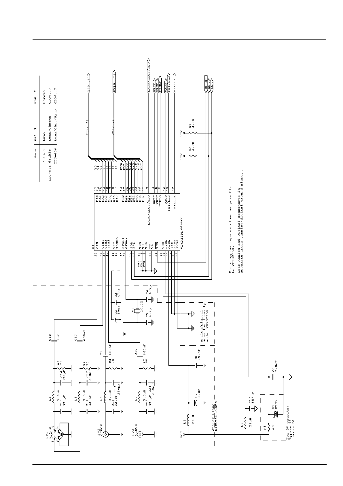
7.5. Typical Application
VPX 3225D, VPX 3224DPRELIMINARY DATA SHEET
85Micronas
Page 86

VPX 3225D, VPX 3224D
PRELIMINARY DATA SHEET
86 Micronas
Page 87

VPX 3225D, VPX 3224DPRELIMINARY DATA SHEET
87Micronas
Page 88

VPX 3225D, VPX 3224D
8. Data Sheet History
1. Preliminary data sheet: “VPX 3225D, VPX 3224D
Video Pixel Decoders”, Edition March 5, 1997,
6251-432-1PD. First release of the preliminary data
sheet.
2. Preliminary data sheet: “VPX 3225D, VPX 3224D
Video Pixel Decoders”, Edition Nov. 9, 1998,
6251-432-2PD. Second release of the preliminary data
sheet. Major changes:
– additional feature: macrovision detection
– format of ITU-R656 ancillary data modified
PRELIMINARY DATA SHEET
– new timing for LLC and OE
pins
– section 3.1.: package outline dimensions changed
Micronas GmbH
Hans-Bunte-Strasse 19
D-79108 Freiburg (Germany)
P.O. Box 840
D-79008 Freiburg (Germany)
Tel. +49-761-517-0
Fax +49-761-517-2174
E-mail: [email protected]
Internet: www.micronas.com
Printed in Germany
Order No. 6251-432-2PD
All information and data contained in this data sheet are without any
commitment, are not to be considered as an offer for conclusion of a
contract, nor shall they be construed as to create any liability . Any new
issue of this data sheet invalidates previous issues. Product availability
and delivery are exclusively subject to our respective order confirmation form; the same applies to orders based on development samples
delivered. By this publication, Micronas GmbH does not assume responsibility for patent infringements or other rights of third parties
which may result from its use.
Further, Micronas GmbH reserves the right to revise this publication
and to make changes to its content, at any time, without obligation to
notify any person or entity of such revisions or changes.
No part of this publication may be reproduced, photocopied, stored on
a retrieval system, or transmitted without the express written consent
of Micronas GmbH.
88 Micronas
Page 89

VPX 3225D, VPX 3224D
Preliminary Data Sheet Supplement
Subject:
Data Sheet Concerned:
New Package for VPX 3225D, VPX 3224D
VPX 3225D, VPX 3224D
6251-432-2PD, Edition Nov. 9, 1998
Supplement:
Edition:
New Package for the VPX 3225D–C3, VPX 3224D–C3
1. The VPX 3225D–C3, VPX 3224D–C3 is also available in the PMQFP44 package.
2. The pinning of the PMQFP44 package has been changed, i.e. mirrored vertically.
3. Production of the PLCC44 package will continue.
Attachment: Package Information VPX 3225D, VPX 3224D
No. 6 / 6251-432-6PDS
April 8, 1999
MICRONAS INTERMETALL page 1 of 4
Page 90
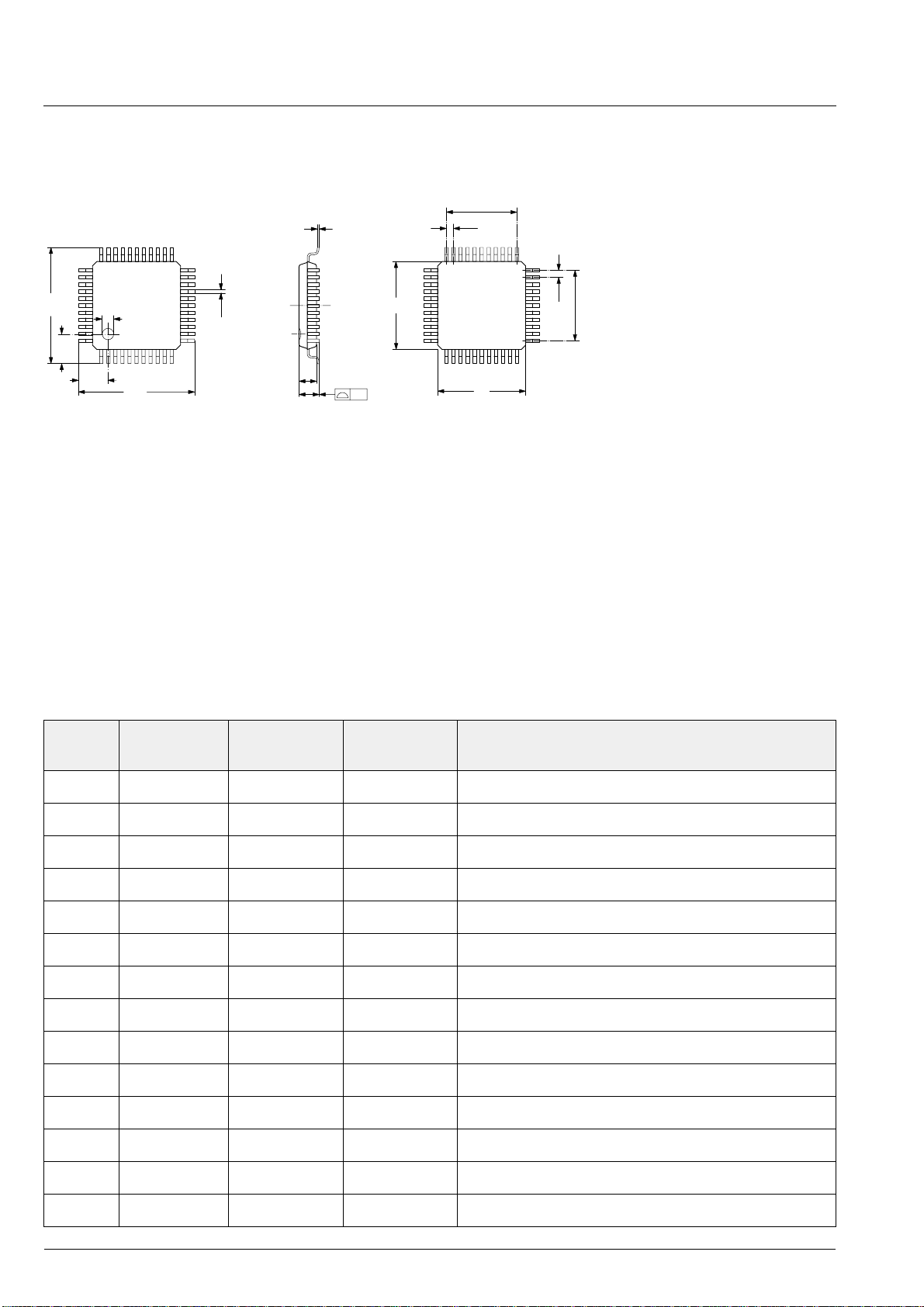
VPX 3225D, VPX 3224D PACKAGE INFORMATION
1. Specifications
1.1. Outline Dimensions
10 x 0.8 = 8
2333
0.17
0.8
13.2
34
1.75
1.3
44
1
1.75
13.2
22
0.375
12
11
2.0
2.15
0.1
Fig. 1–1:
44-Pin Plastic Metric Quad Flat Pack
(PMQFP44)
Weight approx. 0.4 g
Dimensions in mm
1.2. Pin Connections and Short Descriptions
NC = not connected; leave vacant
LV = if not used, leave vacant
X = obligatory
10
10
0.8
10 x 0.8 = 8
D0024/2E
Pin No. Pin Name Pin Type Connection
Short Description
(if not used)
1 VIN1 AIN NC Analog Video 1 Input
2 AVSS SUPPLY X Ground, Analog Circuitry
3 CIN AIN NC Analog Chroma Input
4 AVDD SUPPLY X Supply Voltage, Analog Circuitry
5 XTAL1 OSC IN X Analog Crystal Input
6 XTAL2 OSC OUT X Analog Crystal Output
7 VDD SUPPLY X Supply Voltage, Digital Circuitry
8 VSS SUP PLY X Ground, Digital Circuit ry
9 RESQ IN X Reset Input
2
10 SCL IN/OUT NC I
11 SDA IN/OUT NC I
C Bus Clock
2
C Bus Data
12 B0 OUT NC Port B - Video Data Output
13 B1 OUT NC Port B - Video Data Output
14 B2 OUT NC Port B - Video Data Output
page 2 of 4 MICRONAS INTERMETALL
Page 91
PACKAGE INFORMATION VPX 3225D, VPX 3224D
Pin No. Pin Name Pin Ty pe Connection
(if not used)
Short Description
15 B3 OUT NC Port B - Video Data Output
16 B4 OUT NC Port B - Video Data Output
17 B5 OUT NC Port B - Video Data Output
18 B6 OUT NC Port B - Video Data Output
19 B7 OUT NC Port B - Video Data Output
20 VACT OUT NC Active Video Qualifier Output
21 LLC OUT NC PIXCLK * 2 = 27 MHz Output
22 OEQ IN VSS Output Ports Enable Input
23 A0 OUT NC Port A - Video Data Output
24 A1 OUT NC Port A - Video Data Output
25 A2 OUT NC Port A - Video Data Output
26 A3 OUT NC Port A - Video Data Output
27 PVSS SUPPLY X Ground, Pad Circuits
28 PIXCLK OUT NC Pixel Clock Output
29 PVDD SUPPLY X Supply Voltage Pad Circuits
MICRONAS INTERMETALL page 3 of 4
Page 92
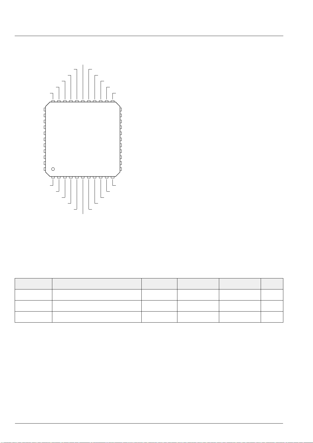
VPX 3225D, VPX 3224D PACKAGE INFORMATION
34
35
36
37
38
39
40
41
42
43
44
22
21
20
19
18
17
16
15
14
13
12
1234567891011
33 32 31 30 29 28 27 26 25 24 23
FIELD
VREF
HREF
TDO (DACT, LLC2)
TCK
TDI
TMS
ISGND
VIN3
VRT
VIN2
OEQ
LLC
VACT
B7
B6
B5
B4
B3
B2
B1
B0
A6
A5
A4
PVDD
PIXCLK
A7
PVSS
A3
A2
A1
A0
AVSS
CIN
AVDD
XTAL1
XTAL2
VIN1
VDD
VSS
RESQ
SCL
SDA
VPX 3225D
VPX 3224D
1.3. Pin Configuration
Fig. 1–2: 44-pin PMQFP package
1.4. Electrical Characteristics
1.4.1. Absolute Maximum Ratings
Symbol Parameter Pin Name Min. Max. Unit
T
A
T
S
T
J
Stresses beyond those listed in the “Absolute Maximum Ratings” may cause permanent damage to the device. This
is a stress rating only. Functional operation of the device at these or any other conditions beyond those indicated in
the “Recommended Operating Conditions/Characteristics” of this specification is not implied. Exposure to absolute
maximum ratings conditions for extended periods may affect device reliability.
Ambient Te mpe ratur e 0 55 °C
Storage Temperature −40 125 °C
Junction Temperature 0 125 °C
page 4 of 4 MICRONAS INTERMETALL
 Loading...