

Page 1

The VP5311/VP5511 converts digital Y, Cr, Cb, data
into analog NTSC/PAL composite video and S-video signals.
The outputs are capable of driving doubly terminated 75
ohm loads with standard video levels.
The device accepts data inputs complying with CCIR
Recommendation 601 and 656. The data is time multiplexed
on an 8 bit bus at 27MHz and is formatted as Y, Cr, Y, Cb
(i.e. 4:2:2). The video blanking and sync information from
REC 656 is included in the data stream when the VP5311/
VP5511 is working in slave mode.
The output pixel rate is 27MHz and the input pixel rate
is half this frequency, i.e. 13.5MHz.
All necessary synchronisation signals are generated
internally when the device is operating in master mode. In
slave mode the device will lock to the TRS codes or the HS
and VS inputs.
The rise and fall times of sync, burst envelope and
video blanking are internally controlled to be within
composite video specifications.
Three digital to analog converters (DACs) are used to
convert the digital luminance, chrominance and composite
data into true analog signals. An internally generated
reference voltage provides the biasing for the DACs.
PIN FUNCTION PIN FUNCTION
1 VDD 33 VDD
2 GND 34 RESET
3 D0 (VS I/O) 35 REFSQ
4 D1 (HS I/O) 36 GND
5 D2 (FC0 O/P) 37 VDD
6 D3 (FC1 O/P) 38 GND
7 D4 (FC2 O/P) 39 PD7
8 D5 40 PD6
9 D6 (SCSYNC I/P) 41 PD5
10 D7 (PALID I/P) 42 PD4
11 GND 43 PD3
12 VDD 44 PD2
13 GND 45 PD1
14 GND 46 PD0
15 PXCK 47 GND
16 VDD 48 VDD
17 CLAMP 49 AGND
18 COMPSYNC 50 VREF
19 GND 51 DACGAIN
20 VDD 52 COMP
21 TDO 53 AVDD
22 TDI 54 LUMAOUT
23 TMS 55 AGND
24 TCK 56 COMPOUT
25 GND 57 AGND
26 SA1 58 CHROMAOUT
27 SA2 59 AVDD
28 SCL 60 N/C
29 VDD 61 N/C
30 SDA 62 AVDD
31 GND 63 AVDD
32 VDD 64 N/C
Figure 1 Pin connections (top view)
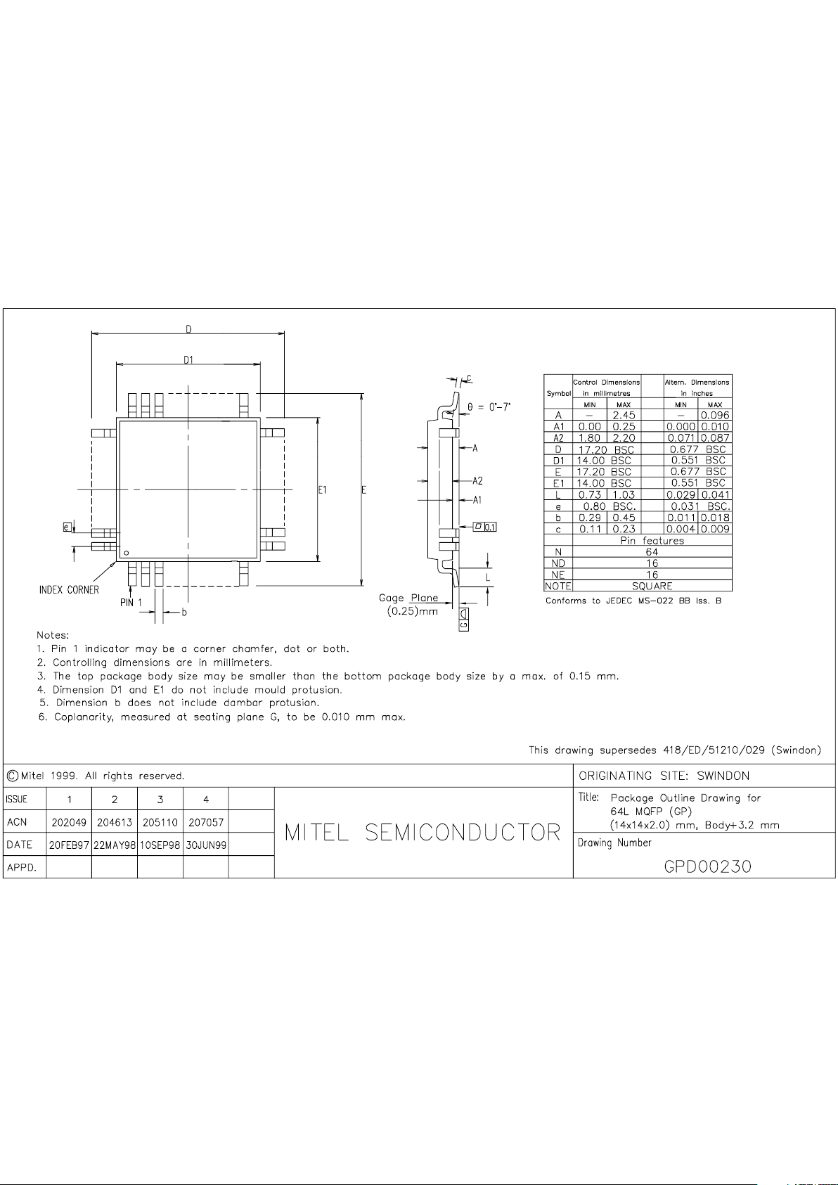
GP64
PIN 64
PIN 1
FEATURES
■ Converts Y, Cr, Cb data to analog composite video and
S-video
■ Supports CCIR recommendations 601 and 656
■ All digital video encoding
■ Selectable master/slave mode for sync signals
■ Switchable chrominance bandwidth
■ Switchable pedestal with gain compensation
■ SMPTE 170M NTSC or CCIR 624 PAL compatible
outputs
■ GENLOCK mode
■ Line 21 Closed Caption encoding
■ I2C bus serial microprocessor interface
■ VP5311B supports Macrovision anti-taping format Rev.
6.1, in PAL and Rev. 7.01 in NTSC.
APPLICATIONS
■ Digital Cable TV
■ Digital Satellite TV
■ Multi-media
■ Video games
■ Karaoke
■ Digital VCRs
ORDERING INFORMATION
VP5311B/CG/GP1N
VP5511B/CG/GP1N
VP5311B/VP5511B
NTSC/PAL Digital Video Encoder
Advance Information
Supersedes DS4575 1.5 May 1997 version DS4575 - 2.2 October 1998
Page 2

VP5311B/VP5511B
2
66.83
1.050
27k
1.3699
24.93
50
33.75
17.64
1.40
7.62
7.62
0.40
34.15
18.71
26.73
8.02
8.02
0.00
ELECTRICAL CHARACTERISTICS
Test conditions (unless otherwise stated): As specified in Recommended Operating Conditions
DC CHARACTERISTICS
VIN
VIL
VIH
VIL
IIH
IIL
VOH
VOL
VOL
2.0
0.7 VDD
3.7
0.8
0.3 VDD
10
-10
0.4
0.6
V
V
V
V
µA
µA
V
V
V
Parameter Conditions
VIN = VDD
VIN = VSS
IOH = -1mA
IOL = +4mA
IOL = +6mA
Symbol Min.
Typ.
Max.
Units
ELECTRICAL CHARACTERISTICS
Test conditions (unless otherwise stated): As specified in Recommended Operating Conditions
DC CHARACTERISTICS DACs
INL
DNL
VREF
ZR
IREF
KDAC
±1.5
±1
±5
LSB
LSB
%
µA
V
Ω
mA
pV-s
mA
mA
mA
mA
mA
mA
mA
mA
mA
mA
mA
mA
Parameter
Symbol Min.
Typ.
Max.
Units
Accuracy (each DAC)
Integral linearity error
Diffential linearity error
DAC matching error
Monotonicity
LSB size
Internal reference voltage
Internal reference voltage output impedance
Reference Current (V
REF/RREF) RREF = 769Ω
DAC Gain Factor (VOUT = KDAC x IREF x RL), VOUT = DAC code 511
Peak Glitch Energy (see fig.3)
CVBS, Y and C - NTSC (pedestal enabled)
Maximum output, relative to sync bottom
White level relative to black level
Black level relative to blank level
Blank level relative to sync level
Colour burst peak - peak
DC offset (bottom sync)
CVBS, Y and C - PAL
Maximum output
White level relative to black level
White level relative to sync level
Black level relative to sync level
Colour burst peak - peak
DC offset (bottom sync)
Digital Inputs TTL compatible (except SDA, SCL)
Input high voltage
Input low voltage
Digital Inputs SDA, SCL
Input high voltage
Input low voltage
Input high current
Input low current
Digital Outputs CMOS compatible
Output high voltage
Output low voltage
Digital Output SDA
Output low voltage
guaranteed
Note: All figures are for: RREF = 769Ω RL = 37.5Ω. When the device is set up in NTSC mode there is a +0.25% error in the PAL
levels. If RL = 75Ω then RREF = 1538Ω.
ABSOLUTE MAXIMUM RATINGS
Supply voltage VDD, AVDD -0·3 to 7·0V
Voltage on any non power pin -0·3 to VDD+0·3V
Ambient operating temperature 0 to 70°C
Storage temperature -55°C to 150°C
Note: Stresses exceeding these listed under Absolute
Maximum Ratings may induce failure. Exposure to Absolute
Maximum Ratings for extended periods may reduce
reliability. Functionality at or above these conditions is not
implied.
Page 3

VP5311B/VP5511B
3
RECOMMENDED OPERATING CONDITIONS
Parameter
Min.
Typ.
Max.
Units
Power supply voltage
Power supply current (including analog outputs)
Input clock frequency
SCL clock frequency
Analog video output load
DAC gain resistor
Ambient operating temperature
Symbol
VDD, AVDD
IDD
PXCK
f
SCL
4.75
-50ppm
0
5.25
+50ppm
500
70
V
mA
MHz
kHz
Ω
Ω
°C
5.00
150
27.00
37.5
769
VIDEO CHARACTERISTICS
Parameter
-61
-56
-58
2.5
2.5
Max.
Symbol Min.
Typ.
5.5
1.3
650
3.57954545
4.43361875
3.58205625
9
10
300
300
145
245
1.5
0.5
-61
-56
-58
-60
10
MHz
MHz
kHz
MHz
MHz
MHz
Fsc cycles
Fsc cycles
ns
ns
ns
ns
% pk-pk
° pk-pk
dB
dB
dB
%
%
dB
ns
Units
ESD COMPLIANCE
Pins
All pins
All pins
Notes
Meets Mil-Std-883 Class 2
Test Levels
2kV on 100pF through 1k5Ω
200V on 200pF through 0Ω & 500nH
Test
Human body model
Machine model
Luminance bandwidth
Chrominance bandwidth (Extended B/w mode)
Chrominance bandwidth (Reduced B/w mode)
Burst frequency (NTSC)
Burst frequency (PAL-B, D,G,H,I)
Burst frequency (PAL-N Argentina)
Burst cycles (NTSC )
Burst cycles (NTSC and PAL-B, D, G, H,I)
Burst envelope rise / fall time (NTSC and PAL-N)
Burst envelope rise / fall time (NTSC and PAL-B, D, G, H,I)
Analog video sync rise / fall time (NTSC and PAL-N)
Analog video blank rise / fall time (NTSC and PAL-B, D, G, H,I)
Differential gain
Differential phase
Signal to noise ratio (unmodulated ramp)
Chroma AM signal to noise ratio (100% red field)
Chroma PM signal to noise ratio (100% red field)
Hue accuracy
Colour saturation accuracy
Residual sub carrier
Luminance / chrominance delay
Page 4

VP5311B/VP5511B
4
Figure 3 Glitch Energy
Figure 2 Functional block diagram of the VP5311B, the VP5511B is identical except there is no Anti-Taping Control
The glitch energy is calculated by measuring the area under the voltage
time curve for any LSB step, typically specified in picoVolt-seconds (pV-s)
Peak Glitch Area = H x W/2
V
t(ps)
W
H
I2C INTERFAC E
SET-UP
REGISTERS
ANTI-TAPING
CONTROL
VIDEO TIMI NG GENERATOR
COLOUR SU BCARRI ER
GENERATOR
MODU LATOR
CHROMA
LOW-PASS
FILTER
INPUT
DEMUX
8
8
PD7-0
D7-0
PXCK
SDA
SCL
SA1
SA2
Y
Cr
Cb
SYNC
BLANK
INSERT
LUMA OU T
COMP
CHROMA OUT
INTERPOLATOR
INTERPOLATOR
JTAG .
GENERAL
PURPOSE PORT
&
CHROMA
INTERP
RESET
CLAMP
CHROMA
DAC
COMP
DAC
OUT
TDI
TMS TCK
TDO
+
DAC
REF
VREF
+
REFSQ
DIGITAL
PHASE COMP
CLOSED
CAPTION
+
DACGAIN
COMP
COMPSYNC
LUMA
DAC
Page 5

VP5311B/VP5511B
5
Pin Name Pin No. Description
PD0-7 39 - 46 8 Bit Pixel Data inputs clocked by PXCK. PD0 is the least significant bit, corresponding to Pin
46. These pins are internally pulled low.
D0-7 3 - 10 8 Bit General Purpose Port input/output. D0 is the least significant bit, corresponding to Pin 3.
These pins are internally pulled low.
PXCK 15 27MHz Pixel Clock input. The VP5311 internally divides PXCK by two to provide the pixel
clock.
CLAMP 17 The CLAMP output signal is synchronised to COMPSYNC output and indicates the position of
the BURST pulse, (lines 10-263 and 273-525 for NTSC; lines 6-310 and 319-623 for PALB,D, G,I,N(Argentina)).
COMPSYNC 18 Composite sync pulse output. This is an active low output signal.
TDO 21 JTAG Data scan output port.
TDI 22 JTAG Data scan input port.
TMS 23 JTAG Scan select input.
TCK 24 JTAG Scan clock input.
SA1 26 Slave address select.
SA2 27 Slave address select.
SCL 28 Standard I
2
C bus serial clock input.
SDA 30 Standard I
2
C bus serial data input/output.
RESET 34 Master reset. This is an asynchronous, active low, input signal and must be asserted for a
minimum 200ns in order to reset the VP5311.
REFSQ 35 Reference square wave input used only during Genlock mode.
VREF 50 Voltage reference output. This output is nominally 1·055V and should be decoupled with a
100nF capacitor to GND.
DAC GAIN 51 DAC full scale current control. A resistor connected between this pin and GND sets the
magnitude of the video output current. An internal loop amplifier controls a reference current
flowing through this resistor so that the voltage across it is equal to the Vref voltage.
COMP 52 DAC compensation. A 100nF ceramic capacitor must be connected between pin 52 and pin
53.
LUMAOUT 54 True luminance, composite and chrominance video signal outputs. These are high
COMPOUT 56 impedance current source outputs. A DC path to GND must exist from each of these pins.
CHROMAOUT 58
NOT USED 60, 61, 64
VDD 1, 12, 16, Positive supply input. All VDD pins must be connected.
20, 29,
32, 33,
37, 48
AVDD 53, 59 Analog positive supply input. All AVDD pins must be connected.
62, 63
GND 2, 11, 13, Negative supply input. All GND pins must be connected.
14, 19,
25, 31,
36, 38, 47
AGND 49, 55, 57 Negative supply input. All AGND pins must be connected.
PIN DESCRIPTIONS
All other pins are N/C and should not be connected.
Page 6

VP5311B/VP5511B
6
5
RA5
ID15
ID0D
ID05
REV5
YCDELAY
CHRBW
DFI2
AN5
SC5
FR15
FR0D
FR05
-
SCH5
CTL5
RD5
WR5
F1W1D5
F1W2D5
F2W1D5
F2W2D5
-
HSOFF5
-
VSMODE
HCNT5
REGISTER
REGISTER
GENLKEN
7
RA7
ID17
ID0F
ID07
REV7
-
-
AN7
SC7
FR17
FR0F
FR07
-
SCH7
CTL7
RD7
WR7
-
-
-
-
-
HSOFF7
-
NCORSTD
HCNT7
FSC4SEL
6
RA6
ID16
ID0E
ID06
REV6
-
CLAMPDIS
AN6
SC6
FR16
FR0E
FR06
-
SCH6
CTL6
RD6
WR6
F1W1D6
F1W2D6
F2W1D6
F2W2D6
-
HSOFF6
-
VBITDIS
HCNT6
GENDITH
4
RA4
ID14
ID0C
ID04
REV4
RAMPEN
SYNCDIS
DFI1
AN4
SC4
FR14
FR0C
FR04
-
SCH4
CTL4
RD4
WR4
F1W1D4
F1W2D4
F2W1D4
F2W2D4
-
HSOFF4
-
F_SWAP
HCNT4
RESERVED
RESERVED
NOLOCK
2
RA2
ID12
ID0A
ID02
REV2
CVBSCLP
LUMDIS
Reserved
AN2
SC2
FR12
FR0A
FR02
-
SCH2
CTL2
RD2
WR2
F1W1D2
F1W2D2
F2W1D2
F2W2D2
F1ST
HSOFF2
-
SL_HS0
HCNT2
TEST
TEST
TSURST
1
RA1
ID11
ID09
ID01
REV1
VFS1
CHRDIS
Reserved
AN1
SC1
FR11
FR09
FR01
-
SCH1
CTL1
RD1
WR1
F1W1D1
F1W2D1
F2W1D1
F2W2D1
F2EN
HSOFF1
HSOFF9
HCNT9
HCNT1
CHRMCLIP
3
RA3
ID13
ID0B
ID03
REV3
SLH&V
BURDIS
DFI0
AN3
SC3
FR13
FR0B
FR03
-
SCH3
CTL3
RD3
WR3
F1W1D3
F1W2D3
F2W1D3
F2W2D3
F2ST
HSOFF3
-
SL_HS1
HCNT3
FOR
FOR
PALIDEN
DEFAULT
hex
13
66
58
05
00
00
00
00
9C
87
C1
F1
00
00
FF
-
00
00
00
00
00
00
7E
00
00
00
00
0
RA0
ID10
ID08
ID00
REV0
VFS0
PEDEN
ACTREN
PARITY
SC0
FR10
FR08
FR00
SCH8
SCH0
CTL0
RD0
WR0
F1W1D0
F1W2D0
F2W1D0
F2W2D0
F1EN
HS0FF0
HSOFF8
HCNT8
HCNT0
TRSEL
R/W
W
R
R
R
R
R/W
R/W
*
R/W
R/W
R/W
R/W
R/W
R/W
R/W
W
R
W
R/W
R/W
R/W
R/W
R/W
R/W
R/W
R/W
R/W
R/W
R/W
R/W
REGISTERS MAP
See Register Details for further explanations.
ADDRESS
hex
00
01
02
03
04
05
06
07
08
09
0A
0B
0C
0D
0E to 1F
20
21
22
23 to EF
F0
F1
F2
F3
F4
F0 to F7
F8
F9
FB
FC
FD
FE
FF
REGISTER
NAME
BAR
PART ID2
PART ID1
PART ID0
REV ID
GCR
VOCR
HANC
ANCID
SC_ADJ
FREQ2
FREQ1
FREQ0
SCHPHM
SCHPHL
Reserved
GPPCTL
GPPRD
GPPWR
Not used
CCREG1
CCREG2
CCREG3
CCREG4
CC_CTL
Reserved
HSOFFL
HSOFFM
SLAVE1
SLAVE2
TEST1
TEST2
GPSCTL
Table.1 Register map
xx = don’t care.
The calculation of the FREQ register value is according to the following formula:-
FREQ = 2
26
x fSC/PXCK hex, where PXCK = 27.00MHz
NTSC value is rounded UP from the decimal number. PAL-B, D, G, H, I and N (Argentina) are rounded DOWN. The SC_ADJ
value is derived from the adjustment needed to be added after 8 fields to ensure accuracy of the Subcarrier frequency. Note the
SC_ADJ value of 9C required for PAL-B, D, G, H, I, is different to the default state of the register.
In NTSC the NCO is reset at the end of every line, this can be disabled by setting the NCORSTD bit in SLAVE1, this allows the
VP5311 to cope with line lengths that are not exactly as specified in REC656.
NOTE * For register HANC, bits 3, 4 and 5 are read only. Bits 1 and 2 are reserved. N/A = not applicable.
For register PART ID0 the VP551 value is AB
Standard
NTSC (default)
PAL-B, G, H, I
PAL-N (Argentina)
FREQ2-0
registers hex
87 C1 F1
A8 26 2B
87 DA 51
Lines/
field
525
625
625
Field
freq. Hz
59.94
50
50
1716
1728
1728
Number of
pixels/line
at 27MHz
15.734266
15.625000
15.625000
Horizontal
freq. kHz.
f
H
3.57954545
4.43361875
3.58205625
Subcarrier
freq. kHz.
fSC
(455/2)
(1135/4+1/625)
(917/4+1/625)
fSC/fH
SC_ADJ
register
hex
xx
9C
57
Table.2 Line, field and subcarrier standards and register settings
Page 7

VP5311B/VP5511B
7
REGISTER DETAILS
BAR Base register
RA7-0 Register address.
PART ID 2-0 Part number
ID17-00 Chip part identification (ID) number.
REV ID Revision number
REV7-0 Chip revision ID number.
GCR Global Control
YCDELAY Luma to Chroma delay.
High = 37ns luma delay, this may be
used to compensate for group delay in
external filters.
Low = normal operation (default).
RAMPEN Modulated ramp enable.
High = ramp output for differential phase
and gain measurements. A 27MHz clock
must be applied to PXCK pin.
Low = normal operation (default).
SL_HS_VS 1 = Slave to HS and VS inputs
CVBSCLMP 1 = Enables clamp on composite output,
to prevent flatenning of chroma peak
throughs
VFS1-0 Video format select
VOCR Video Output Control
CLAMPDIS High = Clamp signal disable
Low = normal operation with clamp signal
enabled (default).
CHRBW Chroma bandwidth select.
High = ±1·3MHz.
Low = ±650kHz (default)
SYNCDIS High = Sync disable (in composite video
signal). COMPSYNC is not affected.
Low = normal operation with sync
enabled (default).
BURDIS High = Chroma burst disable.
Low = normal operation, with burst
enabled (default).
LUMDIS High = Luma input disable - force black
level with synchronisation pulses main-
tained.
Low = normal operation, with Luma input
enabled (default).
CHRDIS High = Chroma input disable - force
monochrome.
Low = normal operation, with Chroma
input enabled (default).
PEDEN High = Pedestal (set-up) enable a
7·5 IRE pedestal on lines 23-262 and
286-525. Valid for NTSC
HANC Horizontal Ancillary Data Control
DFI2-0(read only)Digital Field Identification, 000=Field1
ANCTREN Ancillary timing reference enable. When
High use FIELD COUNT from ancillary
data stream. When low, data is ignored.
ANCID Ancillary data ID
AN7-1 Ancillary data ID
AN0 Parity bit (odd)
Only ancillary data in REC 656 data
stream with the same ID as this byte will
be decoded by the VP5311/VP5511 to
produce H and V synchronisation and
FIELD COUNT.
SC_ADJ Sub Carrier Adjust
SC7-0 Sub carrier frequency seed value, see
table 2.
FREQ2-0 Sub carrier frequency
FR17-00 24 bit Sub carrier frequency programmed
via I
2
C bus, see table 2. FREQ2 is the
most significant byte (MSB).
SCHPHM-L Sub carrier phase offset
SCH9-0 9 bit Sub carrier phase relative to the
50% point of the leading edge of the
horizontal part of composite sync.
SCHPHM bit 0 is the MSB. The nominal
value is zero. This register is used to
compensate for delays external to the
VP5311/VP5511.
GPPCTL General purpose port control
CTL7-0 Each bit controls port direction
Low = output High = input
GPPRD General purpose port read data
RD7-0 I2C bus read from general purpose port
(only INPUTS defined in GPPCTL)
GPPWR General purpose port write data
WR7-0 I2C bus write to general purpose port
(only OUTPUTS defined in GPPCTL)
CCREG1 Closed Caption register 1
F1W1D6-0 Field one (line 21), first data byte
CCREG2 Closed Caption register 2
F1W2D6-0 Field one (line 21), second data byte
CCREG3 Closed Caption register 3
F2W2D6-0 Field two (line 284), first data byte
CCREG4 Closed Caption register 4
F2W2D6-0 Field two (line 284), second data byte
VFS1VFS0
0 0 NTSC (default)
01
PAL-B, D, G,H,I,N(Argentina)
1 0 Reserved
1 1 Reserved
Page 8

VP5311B/VP5511B
8
CCCTL Closed Caption control register
F1ST Field one (line 21) status
High = data has been encoded
Low = new data has been loaded to
CCREG1-2
F2ST Field two (line 284) status
High = data has been encoded
Low = new data has been loaded to
CCREG3-4
F1EN Closed Caption field one (line 21)
High = enable Low = disable (default)
F2EN Closed Caption field two (line 284)
High = enable Low = disable (default)
HSOFFM-L HS offset
HSOFF9-0 This is a 10 bit number which allows the
user to offset the start of digital data input
with reference to the pulse HS.
SLAVE1 H &V Slave mode control register
NCORSTD 1 = NCO Line Reset Disable (NTSC only)
VBITDIS 0 = Video blanked when Rec601 V bit set
1 = V bit is ignored
F_SWAP The odd and even fields are swapped
SL_HS1-0 Selects pixel sample (1 to 4)
HCNT9-8 As HCNT7-0 but MSBs
SLAVE2 H &V Slave position register
HCNT7-0 Adjusts for delay at which pixel data
occurs relative to HS
GPSCTL GPS Control
FSC4SEL When high, REFSQ = 4xFSC and GPP
bit D6 is forced to become an input for a
SCSYNC signal (high = reset), which
provides a synchronous phase reset for
FSC divider. Low = normal operation with
REFSQ = 1xFSC. (default).
GENDITH 1 = Gen lock dither added.
GENLKEN High = enable Genlock to REFSQ signal
input.
Low = internal subcarrier generation
(default).
NOLOCK Genlock status bit (read only)
Low = Genlocked.
High = cannot lock to REFSQ. This bit is
cleared by reading and set again if lock
cannot be attained.
PALIDEN High = enable external PAL ID phase
control and GPP bit D7 is forced to
become an input for PAL ID switch signal,
(GPP bit D7 - Low = +135°,
High = -135°).
Low = normal operation, internal PAL ID
phase switch is used (default).
TSURST High = chip soft reset. Registers are NOT
reset to default values.
Low = normal operation (default).
CHRMCLIP High = enable clipping of chroma data
when luma goes below black level and is
clipped.
Low = no chroma clipping (default).
TRSEL High = master mode, GPP bits D0 - 4 are
forced to become a video timing port with
VS, HS and FIELD outputs.
Low = slave mode, timing from REC656.
I2C BUS CONTROL INTERFACE
I2C bus address
A6
0
A5
0
A4
0
A31A2
1
A0
SA1
A1
SA2
R/ W
X
The serial microprocessor interface is via the bidirectional port consisting of a data (SDA) and a clock (SCL)
line. It is compatible to the Philips I2C bus standard (Jan. 1992
publication number 9398 393 40011). The interface is a slave
transmitter - receiver with a sub-address capability. All
communication is controlled by the microprocessor. The SCL
line is input only. The most significant bit (MSB) is sent first.
Data must be stable during SCL high periods.
A bus free state is indicated by both SDA and SCL lines
being high. START of transmission is indicated by SDA being
pulled low while SCL is high. The end of transmission,
referred to as a STOP, is indicated by SDA going from low to
high while SCL is high. The STOP state can be omitted if a
repeated START is sent after the acknowledge bit. The
reading device acknowledges each byte by pulling the SDA
line low on the ninth clock pulse, after which the SDA line is
released to allow the transmitting device access to the bus.
The device address can be partially programmed by the
setting of the pins SA1 and SA2. This allows the device to
respond to one of four addresses, providing for system
flexibility. The I2C bus address is seven bits long with the last
bit indicating read / write for subsequent bytes.
The first data byte sent after the device address, is the
sub-address - BAR (base address register). The next byte will
be written to the register addressed by BAR and subsequent
bytes to the succeeding registers. The BAR maintains its data
after a STOP signal.
NTSC/PAL Video Standards
Both NTSC (4-field, 525 lines) and PAL (8-field, 625 lines)
video standards are supported by the VP5311/VP5511. All
raster synchronisation, colour sub-carrier and burst
characteristics are adapted to the standard selected. The
VP5311/VP5511 generates outputs which follow the
requirements of SMPTE 170M and CCIR 624 for PAL signals.
The device supports the following:
NTSC,
PAL B, D, G, H, I, N (Argentina).
Page 9

VP5311B/VP5511B
9
Video Blanking
The VP5311/VP5511 automatically performs standard
composite video blanking. Lines 1-9, 264-272 inclusive, as
well as the last half of line 263 are blanked in NTSC mode. In
PAL mode, lines 1-5, 311-318, 624-625 inclusive, as well as
the last half of line 623 are blanked.
The V bit within REC656 defines the video blanking when
TRSEL (bit 0 of GPSCTL register) is set low. When in
MASTER mode with TRSEL set high the video encoder is still
enabled. Therefore if these lines are required to be blank they
must have no video signal input.
Interpolator
The luminance and chrominance data are separately
passed through interpolating filters to produce output
sampling rates double that of the incoming pixel rate. This
reduces the sinx/x distortion that is inherent in the digital to
analog converters and also simplifies the analog
reconstruction filter requirements.
Digital to Analog Converters
The VP5311/VP5511 contained three 9 bit digital to
analog converters which produce the analog video signals.
The DACs use a current steering architecture in which bit
currents are routed to one of two outputs; thus the DAC has
true and complementary outputs. The use of identical current
sources and current steering their outputs means that
monotonicity is guaranteed. An on-chip voltage reference of
1.050V provides the necessary biasing. However, the
VP5311/VP5511 may be used in applications where an
external 1V reference is provided on the VREF pin, to adjust
the video levels. In this case, the external reference should be
temperature compensated and provide a low impedance
output.
The full-scale output currents of the DACs is set by an
external 769Ω resistor between the DACGAIN and GND pins.
An on-chip loop amplifier stabilises the full-scale output
current against temperature and power supply variations.
The analog outputs of the VP5311/VP5511 are capable of
directly driving doubly terminated 75Ω load then the
DACGAIN resistor is simply doubled.
Luminance, Chrominance and Composite Video Outputs
The Luminance video output (LUMAOUT pin 54) drives a
37.5Ω load at 1.0V, sync tip to peak white. It contains only the
luminance content of the image plus the composite sync
pulses. In the NTSC mode, a set-up level offset can be added
during the active video portion of the raster.
The Chrominance video output (CHROMAOUT pin 58)
drives a 37.5Ω load at levels proportional in amplitude to the
luma output (40 IRE pk-pk burst). This output has a fixed offset
current which will produce approximately a 0.5V DC bias
across the 37.5Ω load. Burst is injected with the appropriate
timing relative to the luma signal.
The composite video output (COMPOUT pin 56) will also
drive a 37.5Ω load at 1.0V, sync tip to peak white. It contains
both the luminance and chrominance content of the signal
plus the composite sync pulses.
The CVBS DAC output clipping feature limits the digital
data going into the DAC so that if it goes outside the range it
is limited to the maximum or minimum (511 or 000). This
feature is permanently enabled.
CVBSCLP in register GCR. When set to a '1' this bit
enables an envelope prediction circuit that establishes if the
chroma and luma added together is likely to go outside the
CVBS DAC limits. If it is, then a smooth rounding of the
chroma peaks is made to stop this happening. This prevents
any high frequency components being produced as with the
clipping function which will produce flat peaks. In practice
there will be some loss of saturation in the colour.
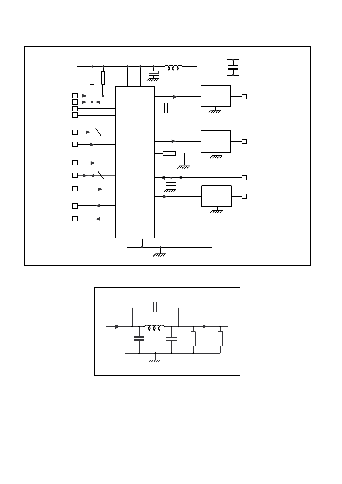
Output sinx/x compensation filters are required on all
video output, as shown in the typical application diagram, see
figs. 8 & 9.
Video Timing - Slave sync mode
The VP5311/VP5511 has an internal timing generator
which produces video timing signals appropriate to the mode
of operation. In the default (power up) slave mode, all timing
signals are derived from the input clock, PXCK, which must be
derived from a crystal controlled oscillator. Input pixel data is
latched on the rising edge of the PXCK clock.
The video timing generator produces the internal blanking
and burst gate pulses, together with the composite sync
output signal, using timing data (TRS codes) from the
Ancillary data stream in the REC656 input signal, (when
TRSEL (bit 0 of GPSCTL register) is set low).
HCNT
To ensure that the incoming data is sampled correctly a 10
bit binary number (HCNT) has to be programmed into the
SLAVE1 and 2 registers. This will allow the device's internal
horizontal counter to align with the video data, each bit
represents one 13.5MHz cycle. To calculate this use the
formula below:
NTSC
HCNT = SN + 119 (SN = 0 - 738)
HCNT = SN + 739 (SN = 739 - 857)
PAL
HCNT = SN + 127 (SN = 0 - 738)
HCNT = SN + 737 (SN = 737 - 863)
where SN is Rec. 656/601 sample number on which the
negative edge of HSYNC occurs.
SL_HS
A further adjustment is also required to ensure that the
correct Cr and Cb sample alignment. The bits SL_HS1-0
allows for four sampling positions in the CbYCrY sequence,
failure to set this correctly will mean corruption of the colour or
colour being interpreted as luma.
F_SWAP
If the field synchronisation is wrong it can be swapped by
setting this bit.
V_SYNC
When set to a '1' this bit allows an odd/even square wave
to provide the field synchronisation.
Example
NTSC
HSYNC occurs on Rec656 sample 721 (end of active
video), then;
HCNT = 721 + 119 = 839 = 348 Hex
SL_HS = 10 (for correct sample)
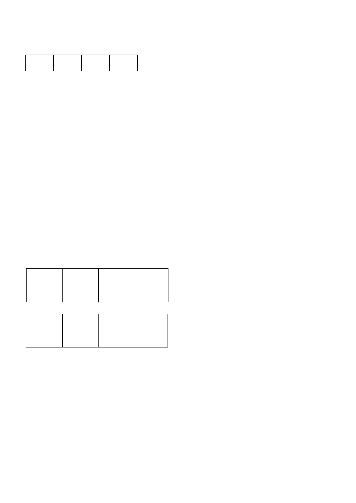
to set slave mode send .04w08pzfbw48pzffw01
Page 10
VP5311B/VP5511B
10
fb
0b
04
08
ff
01
Genlock using REFSQ input
The VP5311 can be Genlocked to another video source by
setting GENLKEN high (in GPSCTL register) and feeding a
phase coherent sub carrier frequency signal into REFSQ.
Under normal circumstances, REFSQ will be the same
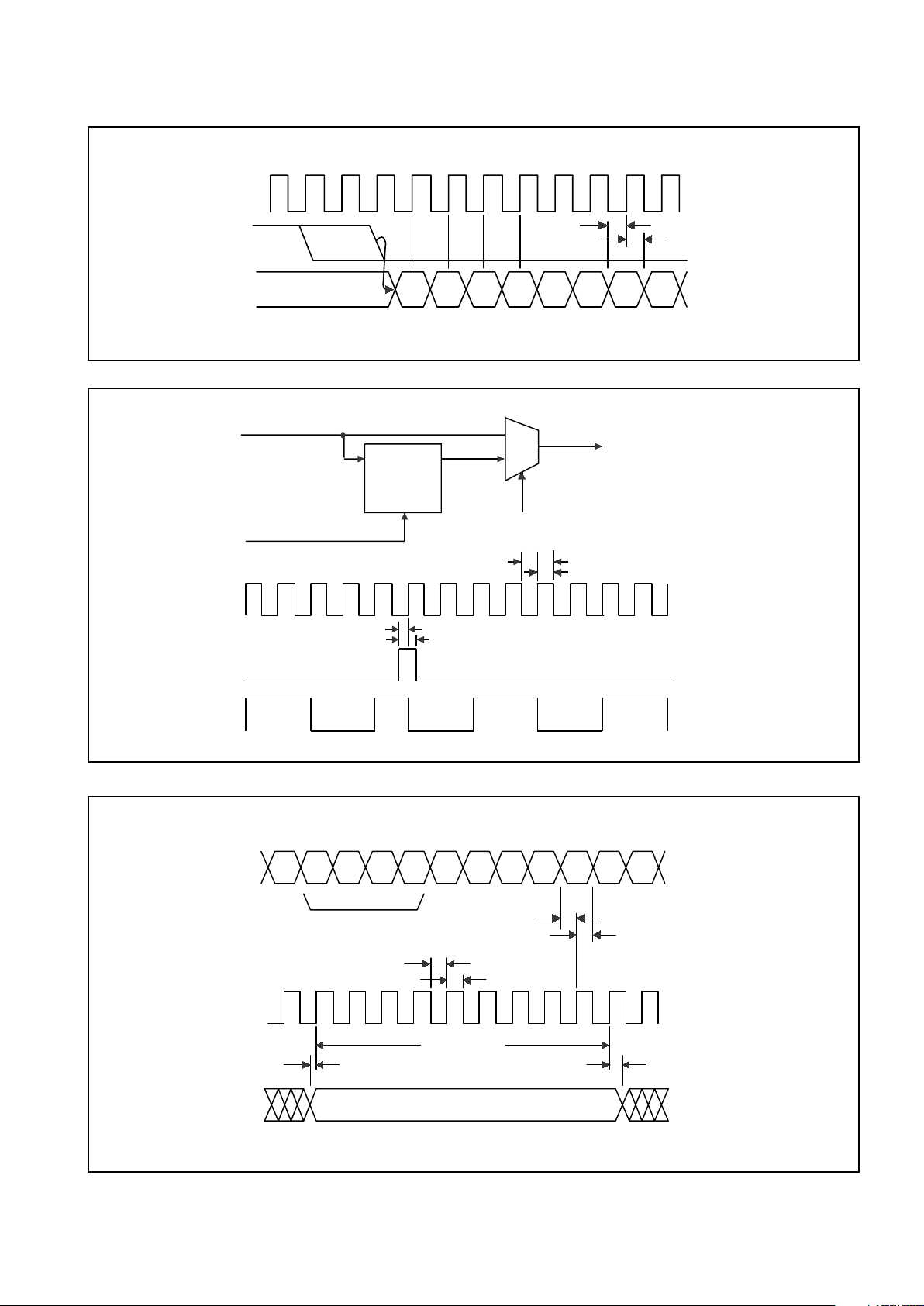
frequency as the sub carrier. But by setting FSC4SEL high (in
GPSCTL register), a 4 x sub carrier frequency signal may be
input to REFSQ. In this case, the Genlock circuit can be reset
to the required phase of REFSQ, by supplying a pulse to
SCSYNC (pin 9). The frequency of SCSYNC can be at sub
carrier frequency, but once per line, or once per field could be
adequate, depending on the application. When GENLKEN is
set high, the direction setting of bit 6 in the GPPCTL register
is igonred.
PALID Input
When in Genlock mode with GENLKEN set high (in
GPSCTL register), the VP5311 requires a PAL phase
identification signal, to define the correct phase on every line.
This is supplied to PALID input (pin 10), High = -135° and low
= +135°. The signal is asynchronous and should be changed
before the sub carrier burst signal. PALID input is enabled by
setting PALIDEN high (in GPSCTL register). When
GENLKEN is high, the direction setting of bit 7 of the GPPCTL
register is ignored
Master Reset
The VP5311/VP5511 must be initialised with the RESET
pin 34. This is an asynchronous active low signal and must be
active for a minimum of 200ns in order for the VP5311/
VP5511 to be reset. The device resets to line 64, start of
horizontal sync (i.e. line blanking active). There is no on-chip
power on reset circuitry.
Line 21 coding
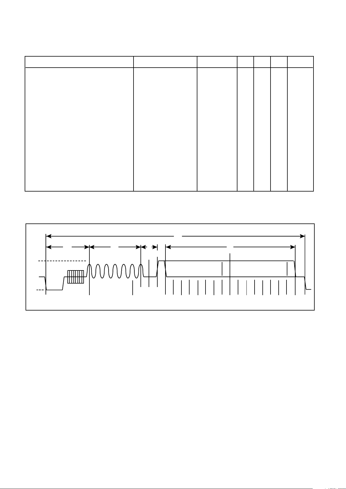
Two bytes of data are coded on the line 21 of each field,
see figure 7. In the NTSC Closed Caption service, the default
state is to code on line 21 of field one only. An additional
service can also be provided using line 21 (284) of the second
field. The data is coded as NRZ with odd parity, after a clock
run-in and framing code. The clock run-in frequency =
0.5034965MHz which is related to the nominal line period, D
= H / 32.
D = 63.55555556 / 32µs
Two data bytes per field are loaded via I
2
C bus registers
CCREG1-4. Each field can be independently enabled by
programming the enable bits in the control register (CC_CTL).
The data is cleared to zero in the Closed Caption shift
registers after it has been encoded by the VP5311/VP5511.
Two status bit are provided (in CC_CTL), which are set high
when data is written to the registers and set low when the data
has been encoded on the Luma signal. The data is cleared to
zero in the Closed Caption shift registers after it has been
encoded by the VP5311/VP5511. The next data bytes must
be written to the registers when the status bit goes high,
otherwise the Closed Caption data output will contain Null
characters. If a transmission slot is missed (ie. no data
received) the encoder will send Null characters. Null
characters are invisible to a closed caption reciever. The MSB
(bit 7) is the parity bit and is automatically added by the
encoder.
this sets registers as follows:
Table.4 for PAL-B, D, G, H, I, N
NCK
0 to 120
121 to 138
184 to 857
HSOFF
126 to 6
863 to 801
800 to 127
Comment
HS normal (64 cks)
HS pulse shortened*
HS normal (64 cks)
Table.3 for NTSC
NCK
0 to 131
132 to 194
195 to 863
HSOFF
137 to 6
869 to 807
806 to 138
Comment
HS normal (64 cks)
HS pulse shortened*
HS normal (64 cks)
reg
data
Note: HSOFF should always be zero when using slave mode.
Video Timing - Master sync mode
When TRSEL (bit 0 of GPSCTL register) is set high, the
VP5311 operates in a MASTER sync mode, all REC656
timing reference codes are ignored and GPP bits D0 - 4
become a video timing port with VS, HS and FIELD outputs.
The PXCK signal is, however, still used to generate all internal
clocks. When TRSEL is set high, the direction setting of bits 4
- 0 of the GPPCTL register is ignored.
VS is the start of the field sync datum in the middle of the
equalisation pulses. HS is the line sync which is used by the
preceding MPEG2 decoder to define when to output digital
video data to the VP5311. The position of the falling edge of
HS relative to the first data Cb0, can be programmed in
HSOFFM-L registers, see fig. 4.
HS offset
The position of the falling edge of HS relative to the first
data Cb0, can be programmed in HSOFFM-L registers, see
figure 4, this is called the pipeline delay and may need
adjusting for a particular application. This is done by
programming a 10 bit number called HSOFF into the
HSOFFM and HSOFFL registers, HSOFFM being the most
significant two bits and HSOFFL the least significant eight bits.
A default value of 07EH is held in the registers.
The value to program into HSOFF can be looked up in
tables 3 &4:
where N
CK = number of 13.5MHz clock cycles between the
falling edge of HS and Cb0 (first data I/P on PD7-0) see fig. 4.
Decreasing HSOFF advances the HS pulse (numbers are in
decimal).
*HS pulse shortened means that the width of the pulse will be
less than the normal 64 13.5MHz clock cycles.
The interruption in the sequence of values is because the HS
signal is jumping across a line boundary to the previous line as
the offset is increased. The register default value is 7EH and
this sets Nck to 0, ie. the HS negative edge and Cb0 are coincident in NTSC mode.
Page 11
VP5311B/VP5511B
11
Figure 5 REFSQ and SC_SYNC input timing
Figure 6 PAL_ID input timing
REFSQ
SC_SYNC
Q
t
SU; SC_SYNC
t
HD; SC_SYNC
1/ f
SC_SYNC
t
PWH; SC_SYNC
Divide by 4
Synchronous
Counter
RESET
REFSQ
SC_SYNC
2:1 mux
Q
FSC4_SEL
f
SC
1
0
Input to
Genlocking
Block
(register bit)
1439 1440 1441 1442 1443 1444 1445 1446 1447 1448 1449 1450
Y719 $FF $00 $XY$00
EAV SEQUENCE
ANCILLARY DATA...
Pixel Data Input (PD[7,0\)
Sample Number
PAL_ID Stable
Input (PAL_ID)
PXCK Input (27MHz)
t
PWH; PXCK
t
PWL; PXCK
t
SU; PD
t
HD; PD
t
HD; PAL_ID
t
SU; PAL_ID
t
DUR; PAL_ID
Figure 4 REC 656 interface with HS output timing
Pixel Data Input (PD[7,0])
PXCK Input (27MHz)
Cb0 Cr0Y0 Y1 Y2 Y3Cb1 Cr1
HS
Nck=0Nck=2
t
SU; PD
t
HD; PD
Page 12
VP5311B/VP5511B
12
TIMING INFORMATION
Min.
Typ.
10
14.5
10
5
10
0
10
0
9
27.0
Max.
TBD
TBD
25
Units
MHz
ns
ns
ns
ns
ns
ns
ns
ns
ns
ns
PXCX
periods
ns
f
PXCK
tPWH; PXCK
tPWL; PXCK
tRP
tFP
tSU;PD
tHD;PD
tSU;SC_SYNC
tHD;SC_SYNC
tSU;PAL_ID
tHD;PAL_ID
tDUR;PAL_ID
tDOS
10% to 90% points
90% to 10% points
PXCK to COMPSYNC
PXCK to CLAMP
Conditions
Parameters
Master clock frequency (PXCK input)
PXCX pulse width, HIGH
PXCX pulse width, LOW
PXCX rise time
PXCX fall time
PD7-0 set up time
PD7-0 hold time
SC_SYNC set up time
SC_SYNC hold time
PAL_ID set up time
PAL_ID hold time
PAL_ID duration
Output delay
Symbol
Note: Timing reference points are at the 50% level. Digital C LOAD <40pF.
Figure 7 Closed Capation format
BIT0 BIT1 BIT2 BIT3 BIT4 BIT5 BIT6 BIT7 BIT0 BIT1 BIT2 BIT3 BIT4 BIT5 BIT6 BIT7
1
CLOCK RUN-IN
START BITS
13
DATA BYTE 1 DATA BYTE 2
0 1 0 0 0 0 1 1
FRAME CODE
B
CD E
A
H
0
50
-40
IRE
HSYNC COLOUR BURST
S1 S2 S3
P
P
P = Parity Bit
Page 13

VP5311B/VP5511B
13
10.250µs
48 IRE
10.500µs
6.5D (12.910µs)
2.0D (3.972µs)
1.0D (1.986µs)
16.0D (31.778µs)
32.0D (63.556)
0.240µs
50 IRE
0 IRE
0 IRE
48 IRE
50 IRE
10.750µs
0.288µs
52 IRE
2 IRE
52 IRE
Encoder minimum
Encoder nominal
Encoder maximum
Description
H-sync to clock run-in
Clock run-in
2, 3
Clock run-in to third start bit
3
Data bit
1, 3
Data characters
4
Horizontal line
1
Rise / fall time of data bit transitions
5
Data bit high (logic level one)
6
Clock run-in maximum
Data bit low (logic level zero)
6
Clock run-in minimum
Data bit differential (high - low)
Clock run-in differential (max. - min)
Interval
A
B
C
D
E
H
Table. 5 Closed Caption data timing. (source EIA R - 4.3 Sept 16 1992)
Notes
1. The Horizontal line frequency f H is nominally 15734.26Hz ±0.05Hz. Interval D shall be adjusted to D = 1/(f H x 32) for the
instantaneous f H at line 21.
2. The clock run-in signal consists of 7.0 cycles of a 0.5034965MHz (1/D) sine wave when measured from the leading to trailing
0 IRE points. The sine wave is to be symmetrical about the 25 IRE level.
3. The negative going midpoints (half amplitude) of the clock run-in shall be coherent with the midpoints (half amplitude) of the
Start and Data bit transitions.
4. Two characters, each consisting of 7 data bits and 1 odd parity bit.
5. 2 T Bar, measured between the 10% and 90% amplitude points.
6. The clock run-in maximum level shall not differ from the data bit high level by more than ±1 IRE. The clock run-in minimum
level shall not differ from the data bit low level by more than ±1 IRE.
Page 14
VP5311B/VP5511B
14
+5V
SCL
SDA
SA1
SA2
I2C
BUS
100µF
VDD, AVDD
GND, AGND
2k2Ω
LUMA
54
58
51
8
PD0-7
REFSQ
PXCK
28
30
26
27
2k2Ω
COMP
CHROMA
DACGAIN
VREF
COMP
OUT
52
CLAMP
COMP
SYNC
CLAMP
COMP
SYNC
17
18
56
PXCK
15
34
3-10
8
GPP
D0-7
50
VDD
GND
10nF
GND
769Ω
SCL
SDA
SA1
SA2
RESET RESET
100nF
REFSQ
VIDEO IN
35
39-46
LUMA OUT
CHROMA OUT
VREF
COMP OUT
OUTPUT
FILTER
OUTPUT
FILTER
OUTPUT
FILTER
AT EVERY
VDD PIN
FERRITE
BEAD
100µF
+5V
Figure 8 Typical application diagram, SLAVE mode. (Output filter - see Fig.9)
Figure 9 Output reconstruction filter
470pF
220pF
1.0µH
GND
75Ω
15pF
EXT
75Ω
Page 15

VP5311B/VP5511B
15
Note:
The VP5311 is only available to customers with a valid and existing authorisation to purchase issued by MACROVISION
CORPORATION.
This device is protected by U.S. patent numbers 4631603, 4577216 and 4819098 and other intellectual property rights. Use of
the Macrovision anticopy process in the device is licensed by Macrovision for non-commercial, home and limited exhibition uses
only. Reverse engineering or disassembly is prohibited.
Page 16
Page 17
Page 18
Page 19

M Mitel (design) and ST-BUS are registered trademarks of MITEL Corporation
Mitel Semiconductor is an ISO 9001 Registered Company
Copyright 1999 MITEL Corporation
All Rights Reserved
Printed in CANADA
TECHNICAL DOCUMENTATION - NOT FOR RESALE
World Headquarters - Canada
Tel: +1 (613) 592 2122
Fax: +1 (613) 592 6909
North America Asia/Pacific Europe, Middle East,
Tel: +1 (770) 486 0194 Tel: +65 333 6193 and Africa (EMEA)
Fax: +1 (770) 631 8213 Fax: +65 333 6192 Tel: +44 (0) 1793 518528
Fax: +44 (0) 1793 518581
http://www.mitelsemi.com
Information relating to products and services furnished herein by Mitel Corporation or its subsidiaries (collectively “Mitel”) is believed to be reliable. However, Mitel assumes no
liability for errors that may appear in this publication, or for liability otherwise arising from the application or use of any such information, product or service or for any infringement of
patents or other intellectual property rights owned by third parties which may result from such application or use. Neither the supply of such information or purchase of product or
service conveys any license, either express or implied, under patents or other intellectual property rights owned by Mitel or licensed from third parties by Mitel, whatsoever.
Purchasers of products are also hereby notified that the use of product in certain ways or in combination with Mitel, or non-Mitel furnished goods or services may infringe patents or
other intellectual property rights owned by Mitel.
This publication is issued to provide information only and (unless agreed by Mitel in writing) may not be used, applied or reproduced for any purpose nor form part of any order or
contract nor to be regarded as a representation relating to the products or services concerned. The products, their specifications, services and other information appearing in this
publication are subject to change by Mitel without notice. No warranty or guarantee express or implied is made regarding the capability, performance or suitability of any product or
service. Information concerning possible methods of use is provided as a guide only and does not constitute any guarantee that such methods of use will be satisfactory in a specific
piece of equipment. It is the user’s responsibility to fully determine the performance and suitability of any equipment using such information and to ensure that any publication or
data used is up to date and has not been superseded. Manufacturing does not necessarily include testing of all functions or parameters. These products are not suitable for use in
any medical products whose failure to perform may result in significant injury or death to the user. All products and materials are sold and services provided subject to Mitel’s
conditions of sale which are available on request.
 Loading...