

Page 1
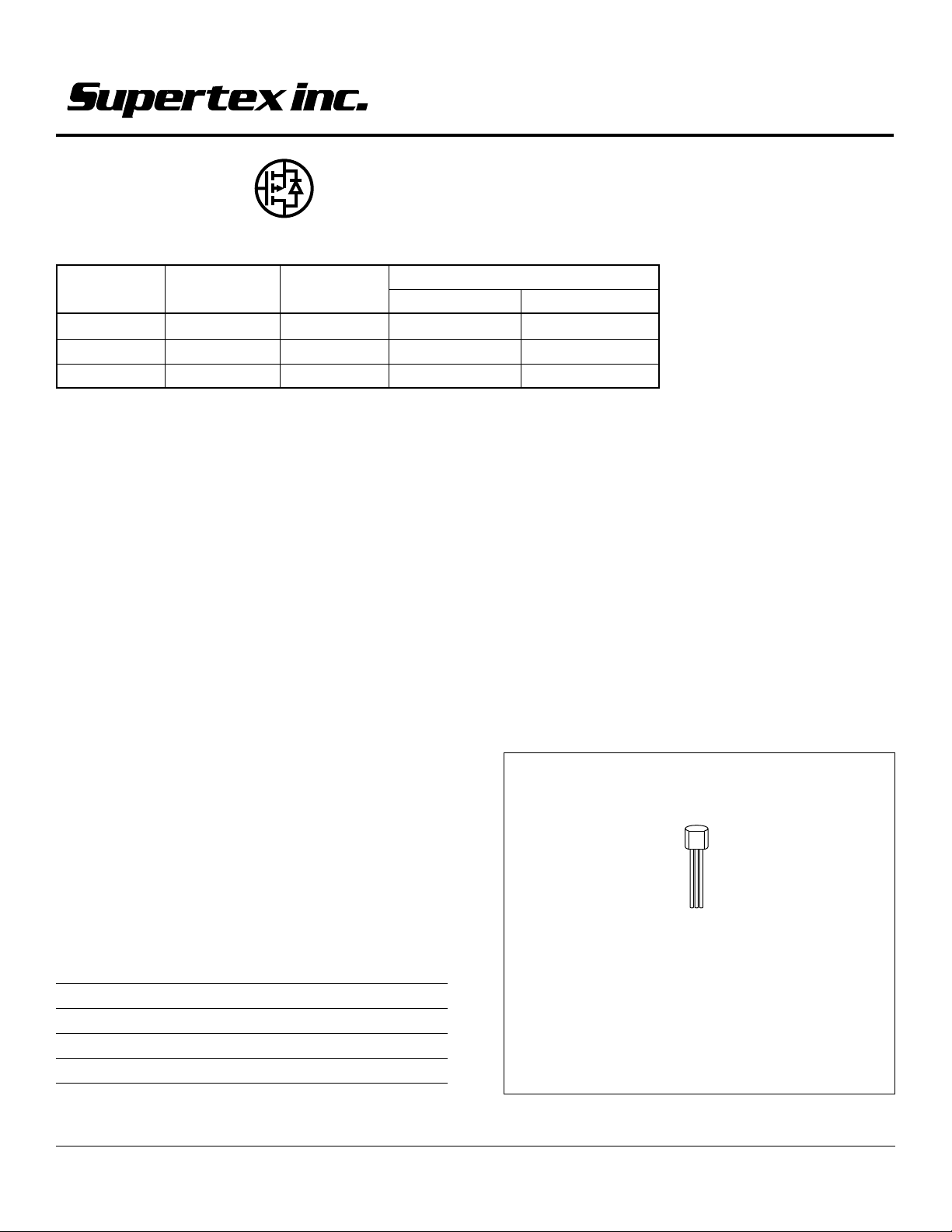
P-Channel Enhancement-Mode
Vertical DMOS FETs
Ordering Information
BV
/R
DSS
BV
DGS
-40V 8.0Ω -0.5A VP0104N3 —
-60V 8.0Ω -0.5A VP0106N3 —
-90V 8.0Ω -0.5A VP0109N3 VP0109ND
DS(ON)
(max) (min) TO-92 Die
I
D(ON)
Order Number / Package
VP0104
VP0106
VP0109
†
Features
❏ Free from secondary breakdown
❏ Low power drive requirement
❏ Ease of paralleling
❏ Low C
❏ Excellent thermal stability
❏ Integral Source-Drain diode
❏ High input impedance and high gain
❏ Complementary N- and P-channel devices
and fast switching speeds
ISS
Applications
❏ Motor controls
❏ Converters
❏ Amplifiers
❏ Switches
❏ Power supply circuits
❏ Drivers (relays, hammers, solenoids, lamps, memories,
displays, bipolar transistors, etc.)
Advanced DMOS Technology
These enhancement-mode (normally-off) transistors utilize a
vertical DMOS structure and Supertex’s well-proven silicon-gate
manufacturing process. This combination produces devices with
the power handling capabilities of bipolar transistors and with the
high input impedance and positive temperature coefficient inherent in MOS devices. Characteristic of all MOS structures, these
devices are free from thermal runaway and thermally-induced
secondary breakdown.
Supertex’s vertical DMOS FETs are ideally suited to a wide range
of switching and amplifying applications where high breakdown
voltage, high input impedance, low input capacitance, and fast
switching speeds are desired.
Package Option
S G D
Absolute Maximum Ratings
Drain-to-Source Voltage BV
Drain-to-Gate Voltage BV
Gate-to-Source Voltage ± 20V
Operating and Storage Temperature -55°C to +150°C
Soldering Temperature* 300°C
* Distance of 1.6 mm from case for 10 seconds.
07/08/02
Supertex Inc. does not recommend the use of its products in life support applications and will not knowingly sell its products for use in such applications unless it receives an adequate "products liability
indemnification insurance agreement." Supertex does not assume responsibility for use of devices described and limits its liability to the replacement of devices determined to be defective due to
workmanship. No responsibility is assumed for possible omissions or inaccuracies. Circuitry and specifications are subject to change without notice. For the latest product specifications, refer to the
Supertex website: http://www.supertex.com. For complete liability information on all Supertex products, refer to the most current databook or to the Legal/Disclaimer page on the Supertex website.
DSS
DGS
Note: See Package Outline section for dimensions.
1
TO-92
Page 2
VP0104/VP0106/VP0109
Thermal Characteristics
Package ID (continuous)* ID (pulsed) Power Dissipation
@ TC = 25°C °C/W °C/W
TO-92 -0.25A -0.8A 1.0W 125 170 -0.25A -0.8A
*
ID (continuous) is limited by max rated Tj.
θ
jc
θ
ja
IDR*I
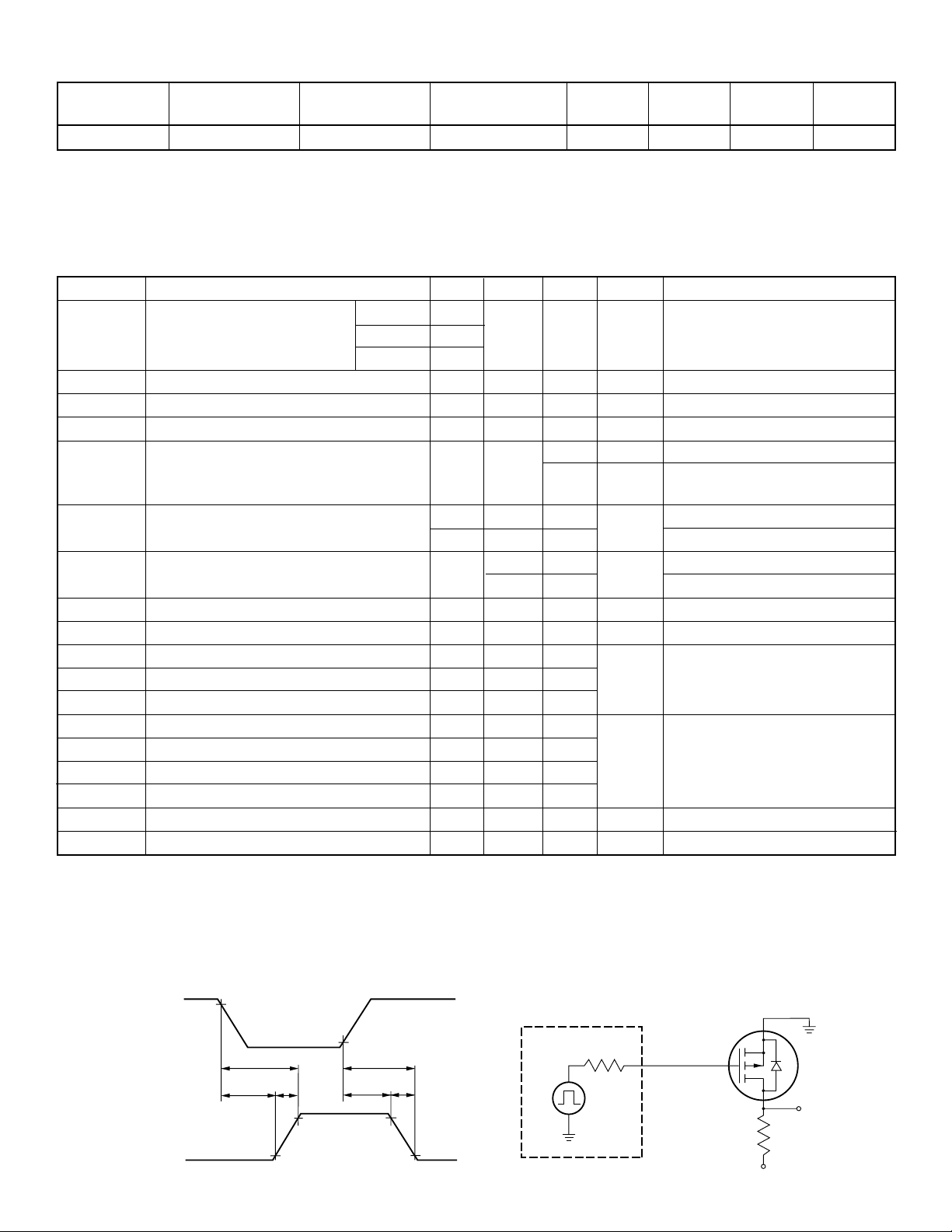
Electrical Characteristics (@ 25°C unless otherwise specified)
Symbol Parameter Min Typ Max Unit Conditions
BV
DSS
Drain-to-Source
Breakdown Voltage
V
GS(th)
∆V
I
GSS
I
DSS
I
D(ON)
R
DS(ON)
GS(th)
Gate Threshold Voltage -1.5 -3.5 V VGS = VDS, ID = -1.0mA
Change in V
with Temperature 5.8 6.5 mV/°CID = -1.0mA, V
GS(th)
Gate Body Leakage -1.0 -100 nA VGS = ±20V, VDS = 0V
Zero Gate Voltage Drain Current -10 µAV
ON-State Drain Current -0.15 -0.25 VGS = -5V, VDS = -25V
Static Drain-to-Source
ON-State Resistance
∆R
DS(ON)
G
FS
C
ISS
C
OSS
C
RSS
t
d(ON)
t
r
t
d(OFF)
t
f
V
SD
t
rr
Notes:
1. All D.C. parameters 100% tested at 25°C unless otherwise stated. (Pulse test: 300µs pulse, 2% duty cycle.)
2. All A.C. parameters sample tested.
Change in R
Forward Transconductance 150 190 m VDS = -25V, ID = -0.5A
Input Capacitance 45 60
Common Source Output Capacitance 22 30 pF
Reverse Transfer Capacitance 3 8
Turn-ON Delay Time 4 6
Rise Time 3 10
Turn-OFF Delay Time 8 12
Fall Time 4 10
Diode Forward Voltage Drop -1.2 -2.0 V ISD = -1.0A, VGS = 0V
Reverse Recovery Time 400 ns ISD = -1.0A, VGS = 0V
with Temperature 0.55 1.0 %/°CV
DS(ON)
VP0109 -90
VP0106 -60
VP0104 -40
-0.50 -1.2 V
VI
-1 mA
= -1.0mA, VGS = 0V
D
= V
GS
= 0V, VDS = Max Rating
GS
= 0V, VDS = 0.8 Max Rating
V
GS
TA = 125°C
A
= -10V, VDS = -25V
GS
11 15 VGS = -5V, ID = -0.1A
6.0 8.0 V
Ω
Ω
= -10V, ID = -0.5A
GS
= -10V, ID = -0.5A
GS
VGS = 0V, VDS = -25V
f = 1 MHz
V
= -25V
DD
ns I
= -0.5A
D
R
GEN
= 25Ω
DS
DRM
Switching Waveforms and Test Circuit
INPUT
OUTPUT
-10V
V
0V
0V
DD
10%
t
d(ON)
t
(ON)
t
r
10%
90%
90%
t
d(OFF)
t
(OFF)
90%
10%
t
F
2
PULSE
GENERATOR
R
gen
INPUT
D.U.T.
OUTPUT
R
L
V
DD
Page 3
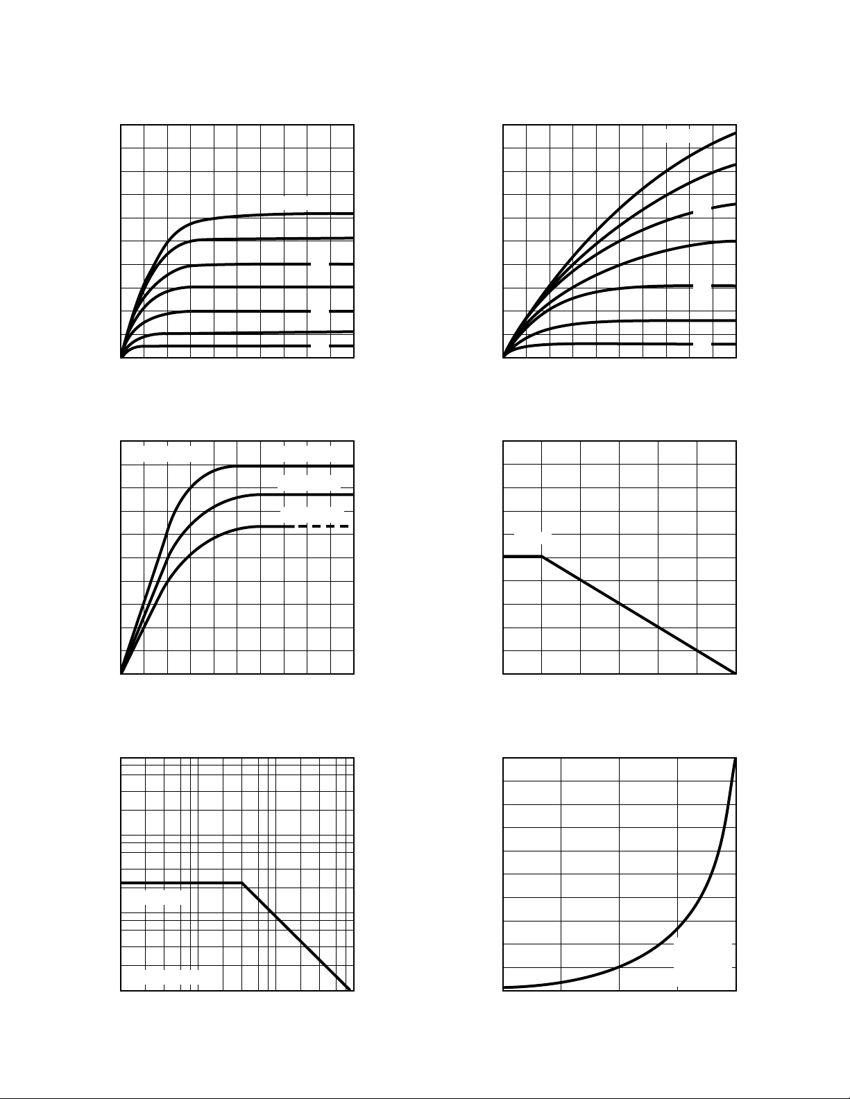
Typical Performance Curves
VP0104/VP0106/VP0109
Output Characteristics
-2.0
-1.6
-1.2
(amperes)
-0.8
D
D
I
-0.4
0
0 -10 -20 -30 -50-40
VDS (volts)
Transconductance vs. Drain Current
250
V
= -25V
DS
200
V
= -10V
GS
TA= -55°C
TA = 25°C
-8V
-6V
-4V
Saturation Characteristics
-1.0
-0.8
-0.6
(amperes)
-0.4
D
I
-0.2
0
0-2-4-6 -10-8
VDS (volts)
Power Dissipation vs. Case Temperature
2.0
V
= -10V
GS
-8V
-6V
-4V
150
(millisiemens)
100
FS
G
50
0
0 -1.0-0.2 -0.4 -0.6 -0.8
ID (amperes)
Maximum Rated Safe Operating Area
-10
-1.0
(amperes)
D
I
TO-92(DC)
-0.1
TA = 125°C
1.0
(watts)
D
P
0
1.0
0.8
0.6
0.4
TO-92
0 15010050
TC (°C)
Thermal Response Characteristics
1257525
-0.01
TC = 25°C
-0.1 -100-10-1.0
VDS (volts)
0.2
Thermal Resistance (normalized)
0
0.001 100.01 0.1 1
3
tp (seconds)
TO-92
P
= 1W
D
TC = 25°C
Page 4
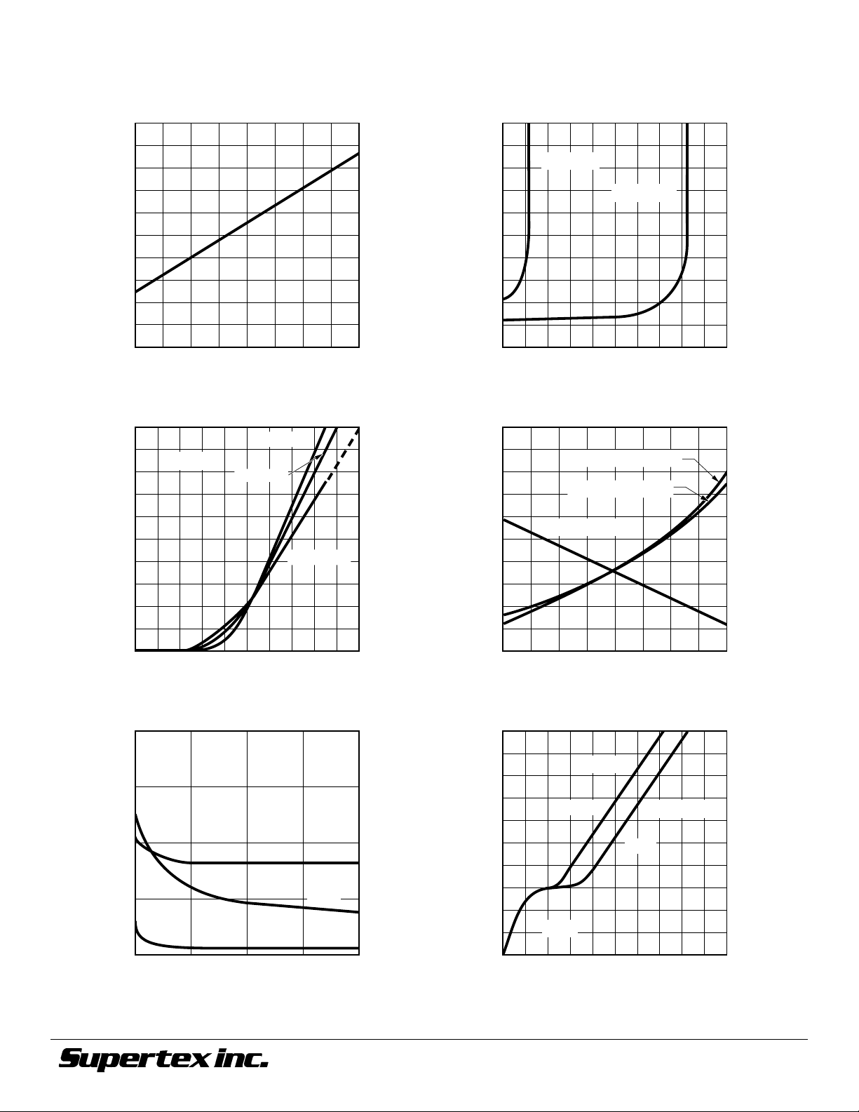
Typical Performance Curves
BV
Variation with Temperature
DSS
DSS
1.10
VP0104/VP0106/VP0109
On-Resistance vs. Drain Current
50
1.06
1.02
(normalized)
0.98
DSS
BV
0.94
0.90
-50 0 50 100 150
Tj (°C)
Transfer Characteristics
-1.0
VDS = -25V
-0.8
-0.6
(amperes)
-0.4
D
I
-0.2
0
0-2-4-6-8-10
V
GS
T
= 25
A
(volts)
°C
= -55
T
A
°C
TA
= 125
°C
40
VGS = -5V
VGS = -10V
30
(ohms)
20
DS(ON)
R
10
0
0 -1.5-0.3 -0.6 -0.9 -1.2
(amperes)
I
D
V
and RDS Variation with Temperature
(th)
1.6
R
@ -10V, -0.5A
1.4
1.2
(normalized)
1.0
GS(th)
V
0.8
0.6
-50 0 50 100 150
DS(ON)
R
DS(ON)
V
@ -1.0mA
(th)
@ -5V, 0.1A
Tj (°C)
1.6
1.4
1.2
1.0
0.8
(normalized)
DS(ON)
R
Capacitance vs. Drain-to-Source Voltage
100
f = 1MHz
75
50
C
ISS
C (picofarads)
25
0
0 -10 -20 -30 -40
C
OSS
C
RSS
VDS (volts)
©2002 Supertex Inc. All rights reserved. Unauthorized use or reproduction prohibited.
Gate Drive Dynamic Characteristics
-10
V
= -10V
-8
-6
(volts)
GS
-4
V
-2
DS
70 pF
70 pF
V
DS
= -40V
45pF
0
0.2 0.4 0.6 0.8 1.00
(nanocoulombs)
Q
G
07/08/02
1235 Bordeaux Drive, Sunnyvale, CA 94089
TEL: (408) 744-0100 • FAX: (408) 222-4895
4
www.supertex.com
 Loading...