

Page 1
VND10BSP
ISO HIGH SIDE SMART POWER SOLID STATE RELAY
TYPE V
VND1 0B SP 40 V 0. 1 Ω 3.4 A 26 V
■ OUTPUTCURRENT(CONTINUOUS):
14A @ T
■ 5V LOGIC LEVEL COMPATIBLEINPUT
■ THERMALSHUT-DOWN
■ UNDERVOLTAGE PROTECTION
■ OPENDRAIN DIAGNOSTIC OUTPUT
■ INDUCTIVELOAD FAST
=85oC PERCHANNEL
c
DSS
R
DS(on
)I
OUT
V
CC
DEMAGNETIZATION
■ VERY LOW STAND-BY POWER
DISSIPATION
DESCRIPTION
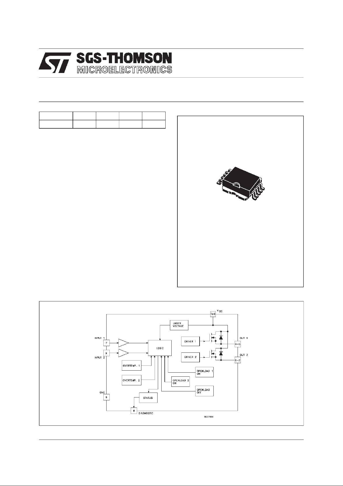
The VND10BSP is a monolithic device made
using SGS-THOMSON Vertical Intelligent Power
Technology, intended for driving resistive or
inductive loads with one side grounded. This
device has two channels, and a common
diagnostic. Built-in thermal shut-down protects
the chip fromover temperatureand shortcircuit.
The statusoutput provides an indicationof open
load in on state, open load in off state,
overtemperatureconditions and stuck-on to V
CC
.
10
1
PowerSO-10
BLOCK DIAGRAM
March 1998
1/9
Page 2
VND10BSP
ABSOLUTEMAXIMUMRATING
Symb o l Para met er Val u e Uni t
V
(BR)DSS
I
OUT
I
(RMS ) RMS Output Curr ent at Tc=85oC and f > 1Hz 14 A
OUT
I
I
-V
I
STAT
V
ESD
P
T
T
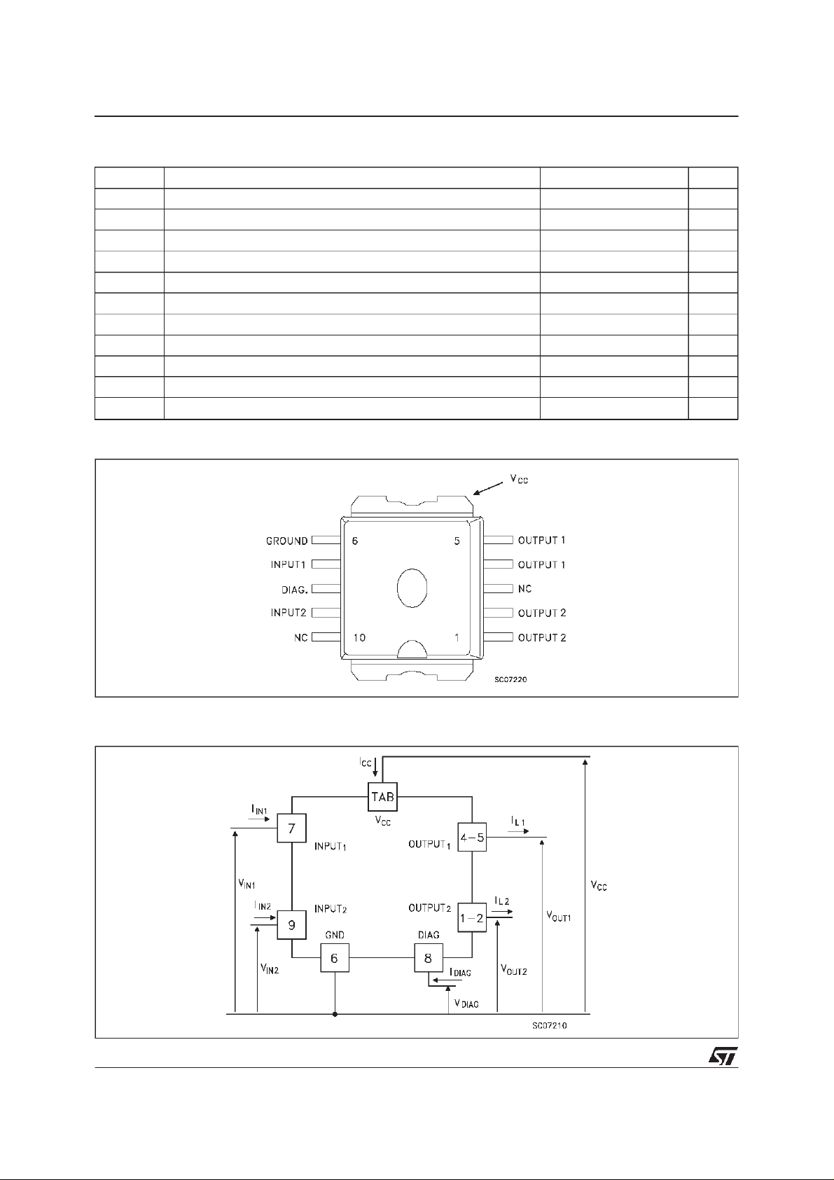
CONNECTION DIAGRAMS
Drain-S o ur ce Br eakdown V olt age 40 V
Out put Current (c on t . ) a t Tc=85oC14A
Revers e Out put Cu rr ent a t Tc=85oC-14A
R
Input Current ±10 mA
IN
Reverse Su pply Voltage -4 V
CC
St at us Current ±10 mA
Elect r o st at ic Disc harge (1.5 kΩ, 100 pF) 2000 V
Power Dissipation at Tc=25oC75W
tot
Junction O per at in g Temperat ure -40 to 150
j
St orage Tem per at ure -55 to 150
stg
o
C
o
C
CURRENT AND VOLTAGE CONVENTIONS
2/9
Page 3

VND10BSP
THERMALDATA
R
thj-case
R
thj-amb
($) When mounted using minimum recommended pad size on FR-4 board
Ther mal Resis t ance Junct io n- case Max
Therm al Res is tance Junction-a mbient ($) Max
1.65
60
ELECTRICAL CHARACTERISTICS (8 < VCC< 16 V; -40 ≤ Tj≤ 125oC unlessotherwise specified)
POWER
Symbol Parameter Test C ondition s Min. Typ. Max. Unit
V
In(*) Nominal Current T
R
I
V
DS(MAX)
R
Supply Voltag e 6 13 26 V
CC
=85oCV
c
On State Resist a nc e I
on
Supply Current Of f St at e Tj=25oCVCC= 13 V 35 100 µA
S
Maximum Voltage Drop I
Out put to GND internal
i
OUT=InVCC
=7.5A Tj=85oCVCC=13V 1.2 2 V
OUT
Tj=25oC51020KΩ
≤ 0.5 VCC=13V 3.4 5.2 A
DS(on)
=13V Tj=25oC 0.065 0.1 Ω
Im pedance
SWITCHING
Symbol Parameter Test C ondition s Min. Typ. Max. Unit
t
(^) Turn- on Delay T im e O f
d(on)
Out put Current
(^) Rise Time O f Output
t
r
Current
(^) Turn- of f Delay Tim e O f
t
d(off)
Out put Current
(^) Fall Time Of Output
t
f
Current
(di/dt)
(di/dt)
Tur n-on Current Slope R
on
Tur n-of f Current S lope R
off
R
=2.7Ω 535200µs
out
R
=2.7Ω 28 110 3 60 µs
out
R
=2.7Ω 10 140 5 00 µs
out
R
=2.7Ω 28 75 360 µs
out
=2.7Ω 0.003 0.1 A / µ s
out
=2.7Ω 0.005 0.1 A / µ s
out
o
o
C/W
C/W
LOGIC INPUT
Symbol Parameter Test C ondition s Min. Typ. Max. Unit
V
V
V
I(hyst.)
I
V
Input Low Level
IL
1.5 V
Volt age
Input High Level
IH
3.5 (•)V
Volt age
Input Hysteresis
0.2 0.9 1.5 V
Volt age
Input Current VIN=5V Tj=25oC30100µA
IN
Input Clamp Volt age IIN=10mA
ICL
=-10mA
I
IN
56
-0.7
7V
V
3/9
Page 4
VND10BSP
ELECTRICAL CHARACTERISTICS (continued)
PROTECTION ANDDIAGNOSTICS
Symbol Parameter Test C ondition s Min. Typ. Max. Unit
V
STAT
V
USD
V
SCL
T
TSD
T
SD(hyst.)
T
V
I
t
povl
t
pol
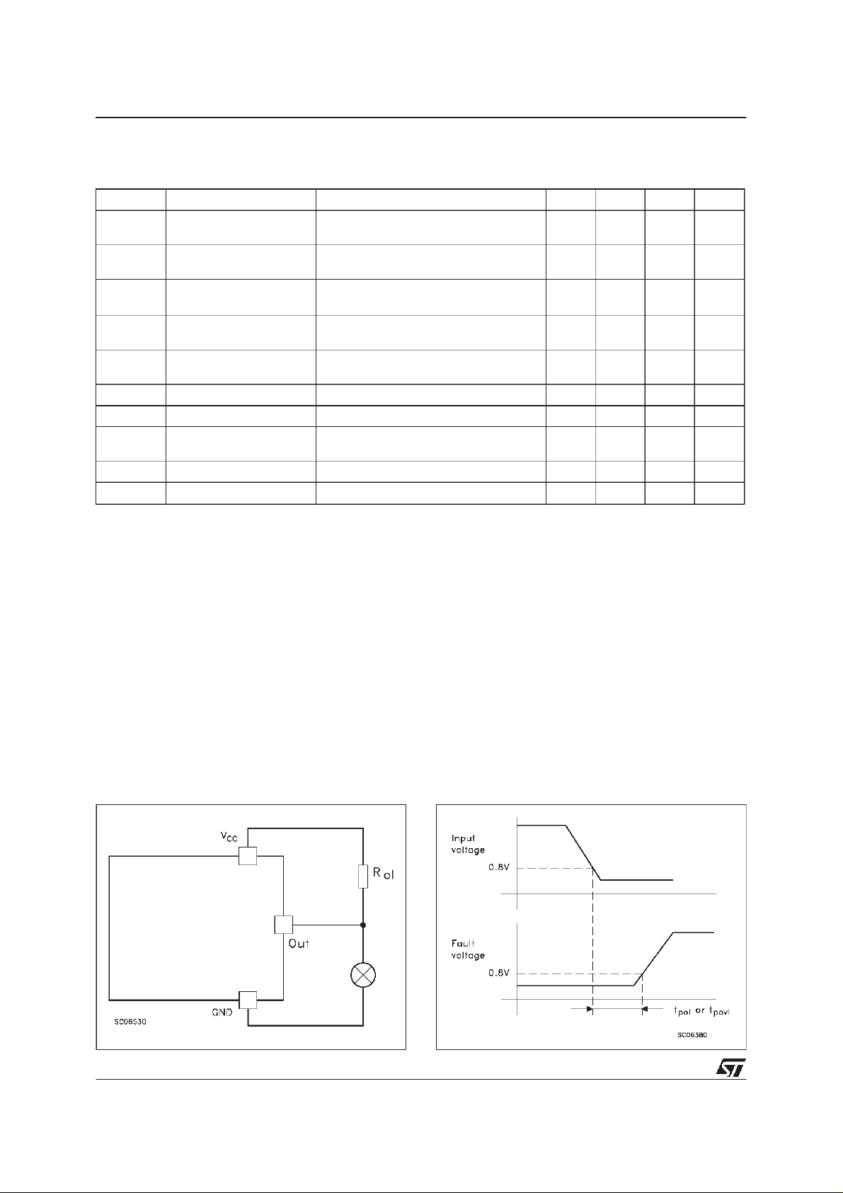
(*) In= Nominal current according to ISO definition for high side automotive switch (see note 1)
NOTE = (^) See switching time waveform
NOTE = (•) The V
calculated to not exceed 10 mA at the input pin.
NOTE = note 1: The Nominal Current is the current at T
NOTE = note 2: I
note 3:t
St at us Voltage Output
I
=1.6mA 0.4 V
STAT
Low
Under Voltage Shut
3.5 4.5 6 V
Down
St at us Clamp Volt age I
Ther mal Shut-down
STAT
I
STAT
=10mA
=-10mA
56
-0.7
140 160 180
Tem perature
Ther mal Shut-down
Hyst eresis
Reset Temperature 125
R
Open Voltage Level Off-State (note 2) 2.5 4 5 V
OL
Open Load Curr ent
OL
On-State 0.6 0.9 1.4 A
Level
St at us Delay (note 3) 5 10 µ s
St at us Delay (note 3) 50 500 2500 µs
is internally clamped at 6V about. It is possible toconnect thispin toan higher voltage via an external resistor
IH
=85oC for battery voltage of 13Vwhich produces a voltage drop of 0.5 V
c
: ISO definition.
povltpol
=(VCC-VOL)/R
OL(off)
OL
7V
50
V
o
C
o
C
o
C
Note2 RelevantFigure Note 3 Relevant Figure
4/9
Page 5
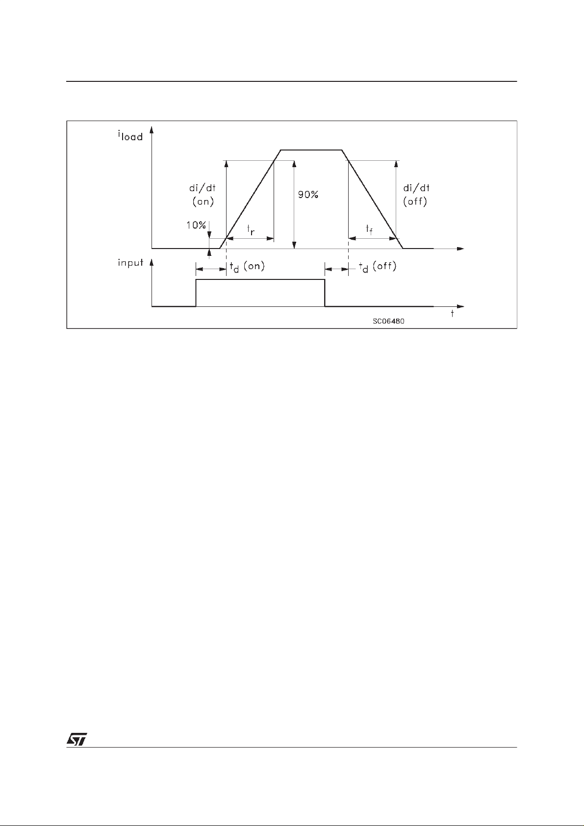
SwitchingTime Waveforms
VND10BSP
FUNCTIONAL DESCRIPTION
The device has a diagnostic output which
indicates open load in on-state, open load in
off-state, over temperature conditions and
stuck-on to V
CC
.
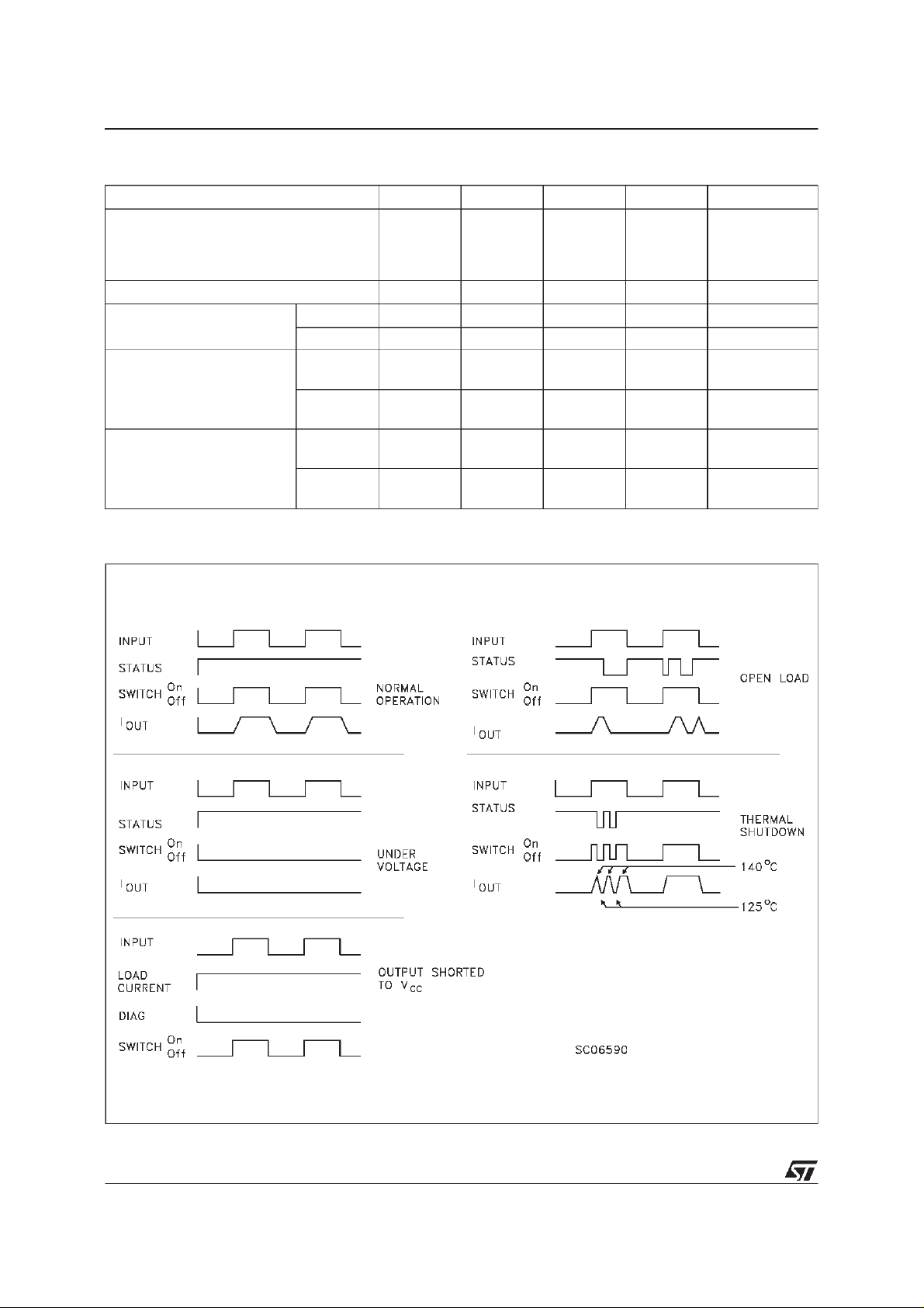
From the falling edge of the input signal, the
status output, initially low to signal a fault
condition (overtemperature or open load
on-state), will go back to a high state with a
different delay in case of overtemperature (tpovl)
and in case of open open load (tpol)respectively.
This feature allows to discriminate the nature of
the detected fault. To protect the device against
short circuit and over current condition, the
thermal protection turns the integrated Power
MOS off at a minimum junction temperature of
140oC. When this temperature returns to 125oC
the switch is automatically turned on again. In
short circuit the protection reacts with virtually no
delay, the sensor being located inside the Power
MOS area. An internal function of the devices
ensures the fast demagnetization of inductive
loads with a typicalvoltage (V
) of-18V. This
demag
function allows to greatly reduces the power
dissipationaccordingto the formula:
P
dem
= 0.5• L
load
•(Ι
load
)2• [(VCC+V
demag
)/V
demag
• f
where f =switching frequencyand
V
=demagnetizationvoltage.
demag
The maximum inductance which causes the chip
temperature to reach the shut-down temperature
in a specifiedthermal environment is a function of
the load current for a fixed V
CC
,V
according to the above formula. In this device if
the GND pin is disconnected, with V
exceeding16V, it willswitch off.
PROTECTING THE DEVICE AGAINST
REVERSE BATTERY
The simplest way to protect the device against a
continuous reverse battery voltage (-26V) is to
insert a Schottky diode between pin 1 (GND) and
ground, as shown in the typical application circuit
(fig.3).
The consequences of the voltage drop across
this diode areas follows:
If the input is pulled to power GND, a negative
voltage of -V
is seen by the device. (Vil, Vih
f
thresholds and Vstat are increased by Vf with
respectto power GND).
Theundervoltageshutdown level is increa- sed
byVf.
If there is no need for the control unit to handle
external analog signals referred to the power
GND, the best approach is to connect the
]
referencepotential of the controlunit to node [1]
(see application circuit in fig. 3), which becomes
the common signal GND for the whole control
board avoiding shift of V
,Viland V
ih
solutionallows the use of a standarddiode.
demag
stat
and f
CC
. This
not
5/9
Page 6
VND10BSP
TRUTH TABLE
INPUT 1 INPU T 2 OUT PUT 1 O UT PUT 2 DIAGNOS TI C
Normal Opera ti on L
H
L
H
Under-voltage X X L L H
Thermal Shutdown
Open Load
Out put Shorted t o V
(**) with additional external resistor.
CC
Channel1
Channel2
Channel1
Channel2
Channel1
Channel2
HXLX L
XHXL L
H
L
X
L
H
L
X
L
Figure1: Waveforms
L
H
H
L
X
L
H
L
X
L
H
L
L
H
L
H
H
L
X
L
H
H
X
L
L
H
H
L
X
L
H
L
X
L
H
H
H
H
H
H
L
L(**)
L
L(**)
L
L
L
L
6/9
Page 7
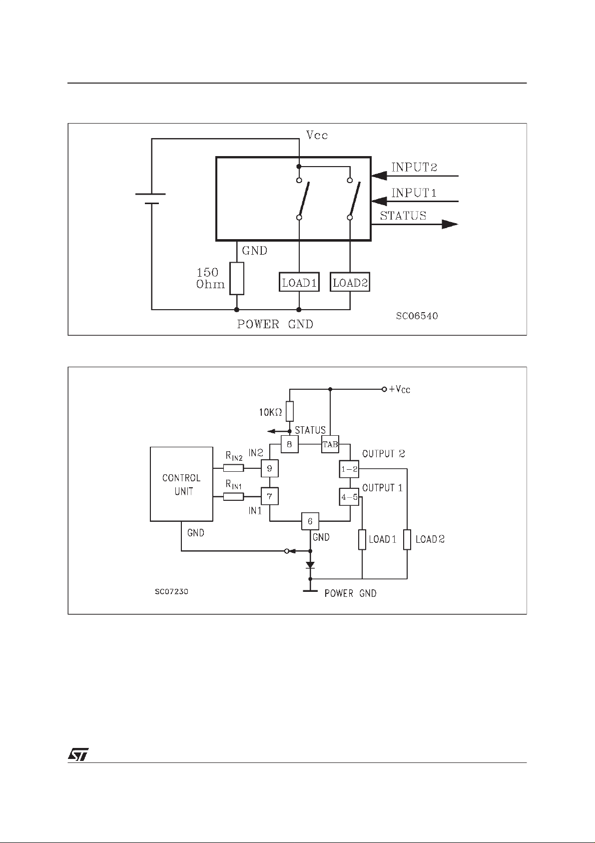
Figure2: Typical ApplicationCircuit With ASchottkyDiode For Reverse SupplyProtection
Figure3: Typical ApplicationCircuit With Separate Signal Ground
VND10BSP
7/9
Page 8
VND10BSP
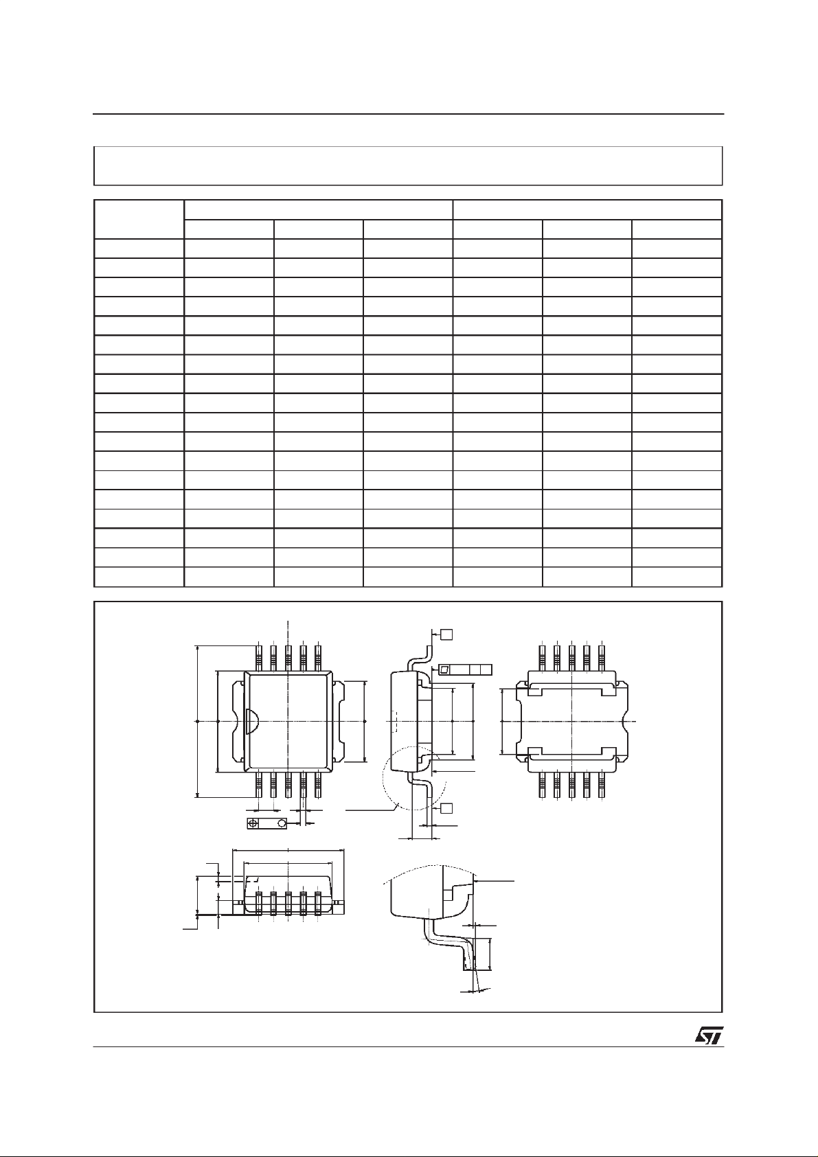
PowerSO-10 MECHANICAL DATA
DIM.
mm inch
MIN. TYP. MAX. MIN. TYP. MAX.
A 3.35 3.65 0.132 0.144
A1 0.00 0.10 0.000 0.004
B 0.40 0.60 0.016 0.024
c 0.35 0.55 0.013 0.022
D 9.40 9.60 0.370 0.378
D1 7.40 7.60 0.291 0.300
E 9.30 9.50 0.366 0.374
E1 7.20 7.40 0.283 0.291
E2 7.20 7.60 0.283 0.300
E3 6.10 6.35 0.240 0.250
E4 5.90 6.10 0.232 0.240
e 1.27 0.050
F 1.25 1.35 0.049 0.053
H 13.80 14.40 0.543 0.567
h 0.50 0.002
L 1.20 1.80 0.047 0.071
q 1.70 0.067
α 0
o
o
8
==
==
HE
h
A
F
A1
610
51
eB
M
0.25
D
==
D1
==
DETAIL”A”
E2
==
DETAIL”A”
Q
B
0.10 A
E1E3
==
SEATING
PLANE
A
C
α
B
E4
==
SEATING
PLANE
A1
L
==
0068039-C
8/9
Page 9

VND10BSP
Information furnished isbelieved to be accurate and reliable. However, SGS-THOMSON Microelectronics assumes no responsability for the
consequences of use ofsuch information nor for anyinfringement of patents or other rights of third parties which may resultsfrom itsuse. No
license is granted by implication or otherwiseunder any patent orpatent rights of SGS-THOMSON Microelectronics. Specifications mentioned
in this publication are subjectto changewithout notice.This publicationsupersedes and replaces all information previously supplied.
SGS-THOMSON Microelectronicsproducts are notauthorized foruse as criticalcomponents in lifesupport devices orsystems without express
written approval of SGS-THOMSON Microelectonics.
1998 SGS-THOMSON Microelectronics - Printedin Italy -All RightsReserved
Australia - Brazil - Canada -China - France - Germany - Italy - Japan- Korea- Malaysia - Malta - Morocco -The Netherlands -
Singapore - Spain - Sweden- Switzerland- Taiwan -Thailand - United Kingdom -U.S.A
SGS-THOMSON MicroelectronicsGROUP OF COMPANIES
...
9/9
 Loading...