

Page 1
VNB10N07/K10N07FM
VNP10N07FI/VNV10N07
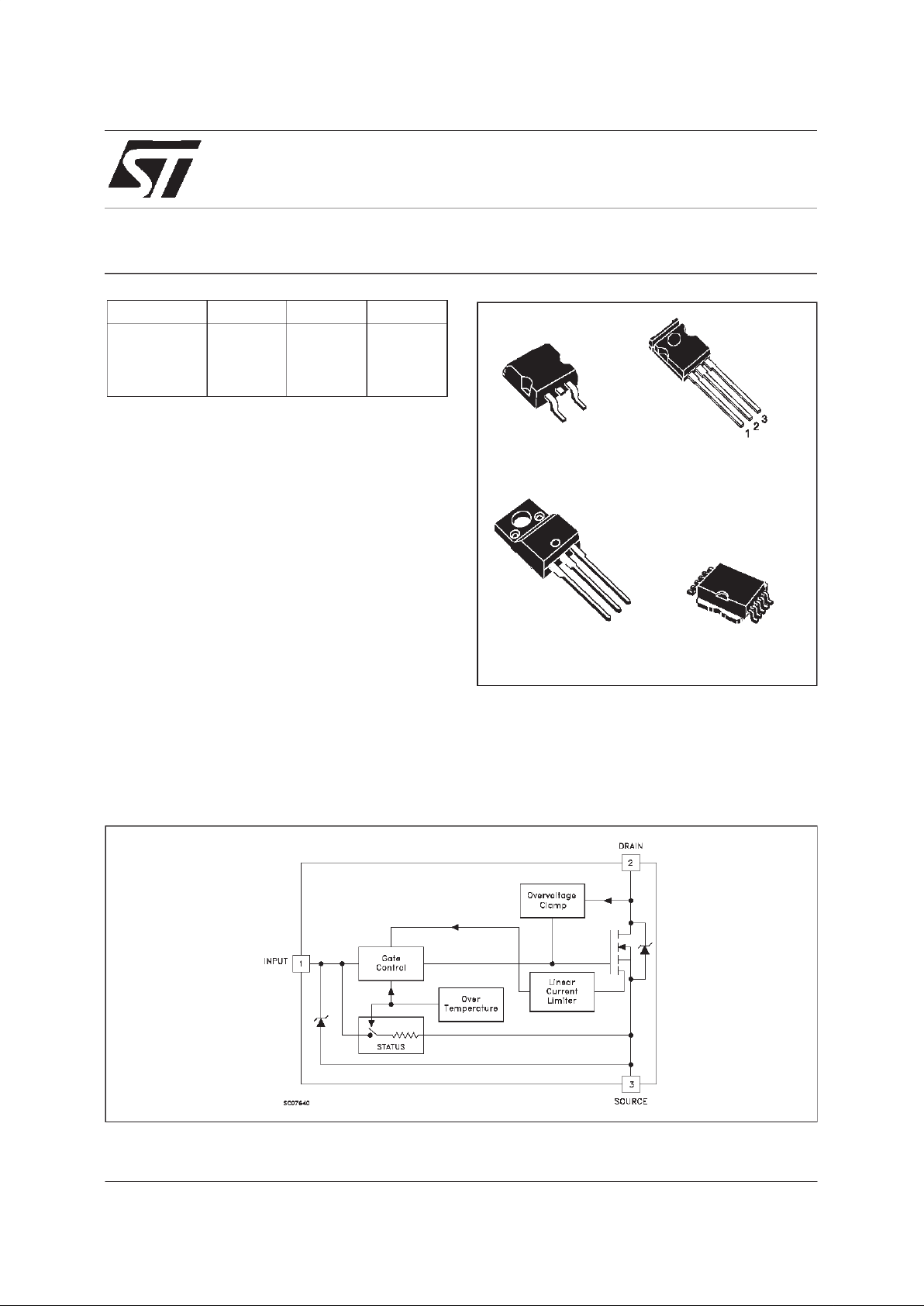
”OMNIFET”:
FULLY AUTOPROTECTED POWER MOSFET
June 1998
BLOCK DIAGRAM (∗)
TYPE V
clamp
R
DS(on)
I
lim
VNB10N07
VNK10N07FM
VNP10N07FI
VNV10N07
70 V
70 V
70 V
70 V
0.1 Ω
0.1 Ω
0.1 Ω
0.1 Ω
10 A
10 A
10 A
10 A
■ LINEAR CURRENT LIMITATION
■ THERMALSHUTDOWN
■ SHORTCIRCUIT PROTECTION
■ INTEGRATEDCLAMP
■ LOW CURRENT DRAWN FROM INPUT PIN
■ DIAGNOSTICFEEDBACK THROUGH INPUT
PIN
■ ESD PROTECTION
■ DIRECT ACCESS TO THE GATE OF THE
POWERMOSFET(ANALOGDRIVING)
■ COMPATIBLEWITHSTANDARD POWER
MOSFET
DESCRIPTION
The VNB10N07, VNK10N07FM, VNP10N07FI
and VNV10N07 are monolithic devices made
using STMicroelectronics VIPower M0
Technology, intended for replacement of
standard power MOSFETS in DC to 50 KHz
applications. Built-in thermal shut-down, linear
current limitation and overvoltage clamp protect
the chip in harsh enviroments.
Faultfeedback can be detected by monitoringthe
voltageat the input pin.
1
10
PowerSO-10
1
3
1
2
3
ISOWATT220
D2PAK
TO-263
SOT82-FM
(∗) PowerSO-10 PinConfiguration : INPUT = 6,7,8,9,10; SOURCE = 1,2,4,5; DRAIN = TAB
1/14
Page 2
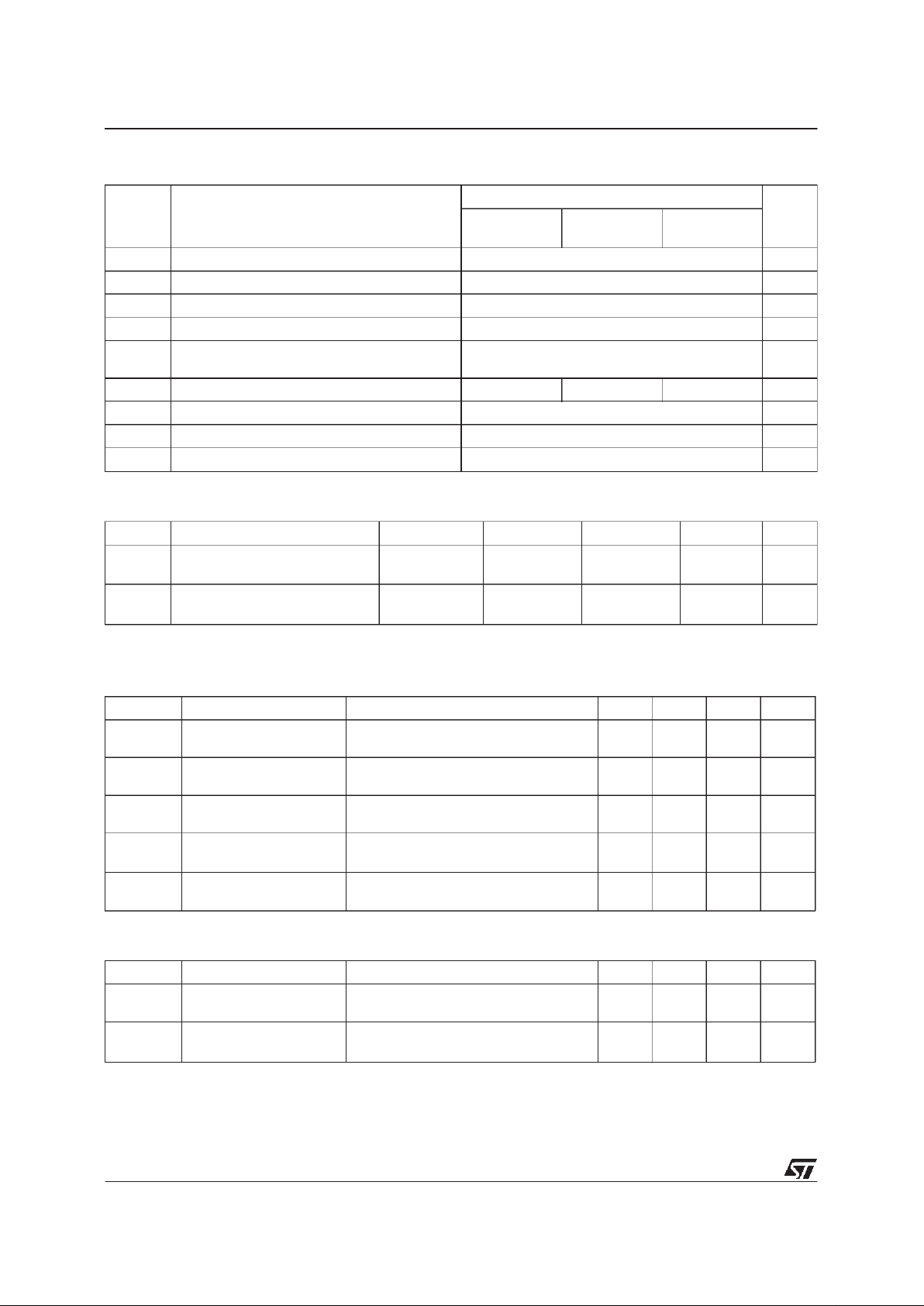
ABSOLUTEMAXIMUMRATING
Symbol Parameter Value Unit
PowerS O -10
D2PAK
SOT-82FM ISOWATT220
V
DS
Drain-source Voltage (Vin= 0 ) Internally C lam ped V
V
in
Input Voltage 18 V
I
D
Drain Current Inte r nally Limited A
I
R
Reverse DC Output Current -14 A
V
esd
Elect r os t at ic Discha rge (C= 100 pF,
R=1. 5 KΩ)
2000 V
P
tot
Tot al Dis sipa t ion at Tc=25oC509.531W
T
j
Oper at ing Junction T em perature Inte r nally Limited
o
C
T
c
Case Operating Temperature Internally Limited
o
C
T
stg
Sto rage Tem perat ure -55 to 150
o
C
THERMAL DATA
ISOWATT220 Po werSO-10 SOT82-FM D 2PAK
R
thj-case
Ther mal Resistance
Junct ion-case Max 4 2.5 13 2.5
o
C/W
R
thj-amb
Ther mal Resistance
Junct ion-ambie nt Max 62.5 50 100 62.5
o
C/W
ELECTRICAL CHARACTERISTICS (T
case
=25oC unlessotherwise specified)
OFF
Symbol Parameter Test Cond itions Mi n. Typ. Max. Unit
V
CLAMP
Drain-source Clamp
Volt age
ID= 200 mA Vin= 0 60 70 80 V
V
CLTH
Drain-source Clamp
Thr eshold V ol ta ge
ID=2mA Vin=0 55 V
V
INCL
Input-Source Reverse
Clamp Voltage
Iin=-1mA -1 -0.3 V
I
DSS
Zer o I npu t V olt age
Drain Current (V
in
=0)
V
DS
=13V Vin=0
V
DS
=25V Vin=0
50
200
µA
µA
I
ISS
Supply Current from
Input Pin
VDS=0V Vin= 10 V 250 500 µA
ON (∗)
Symbol Parameter Test Cond itions Mi n. Typ. Max. Unit
V
IN(th)
Input Thres hold
Volt age
VDS=VinID+Iin=1mA 0.8 3 V
R
DS(on)
St at ic Drain-s our ce On
Resistance
Vin=10V ID=5A
V
in
=5V ID=5A
0.1
0.14
Ω
Ω
VNB10N07-VNK10N07FM-VNP10N07FI-VNV10N07
2/14
Page 3
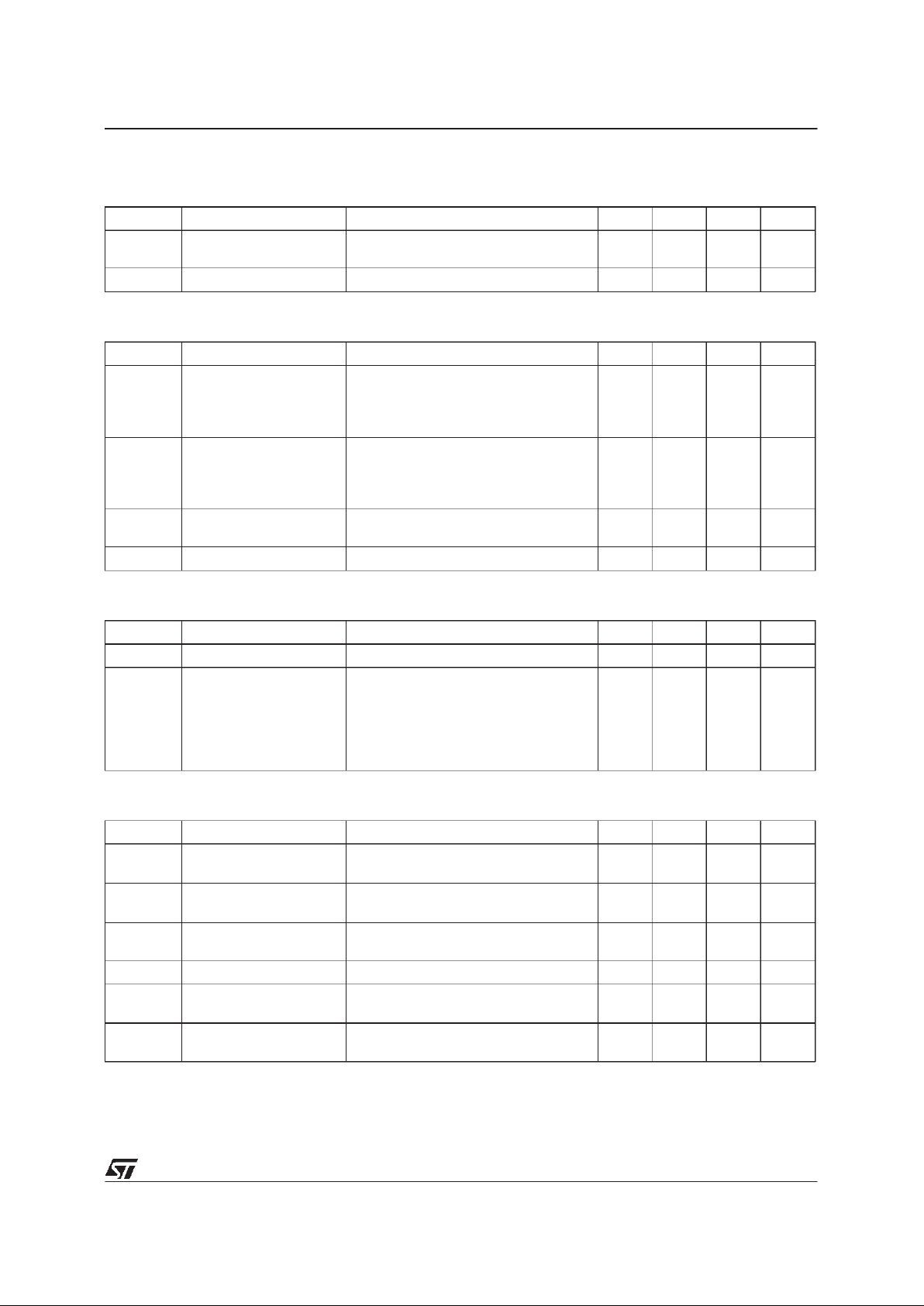
ELECTRICAL CHARACTERISTICS (continued)
DYNAMIC
Symbol Parameter Test Cond itions Mi n. Typ. Max. Unit
g
fs
(∗)Forward
Tr ansc on ductance
VDS=13V ID=5A 6 8 S
C
oss
Out put Capacit anc e VDS = 13 V f = 1 MH z Vin= 0 350 5 00 pF
SWITCHING(**)
Symbol Parameter Test Cond itions Mi n. Typ. Max. Unit
t
d(on)
t
r
t
d(off)
t
f
Turn-on Delay Time
Rise Time
Turn-off Delay T ime
Fall T ime
VDD=15V Id=5A
V
gen
=10V R
gen
=10Ω
(see figure 3)
50
80
230
100
100
160
400
180
ns
ns
ns
ns
t
d(on)
t
r
t
d(off)
t
f
Turn-on Delay Time
Rise Time
Turn-off Delay T ime
Fall T ime
VDD=15V Id=5A
V
gen
=10V R
gen
= 1000 Ω
(see figure 3)
600
0.9
3.8
1.7
900
2
6
2.5
ns
µs
µs
µs
(di/dt)
on
Tur n-on Current Slope VDD=15V ID=5A
V
in
=10V R
gen
=10Ω
60 A/µs
Q
i
Total Input Charge VDD=12V ID=5A Vin= 10 V 30 nC
SOURCE DRAIN DIODE
Symbol Parameter Test Cond itions Mi n. Typ. Max. Unit
V
SD
(∗)ForwardOnVoltage ISD=5A Vin=0 1.6 V
t
rr
(∗∗)
Q
rr
(∗∗)
I
RRM
(∗∗)
Reverse Re covery
Time
Reverse Re covery
Charge
Reverse Re covery
Current
I
SD
= 5 A di/dt = 100 A/µs
V
DD
=30V Tj=25oC
(see test cir cuit, figure 5)
125
0.3
4.8
ns
µC
A
PROTECTION
Symbol Parameter Test Cond itions Mi n. Typ. Max. Unit
I
lim
Drain Current Limit Vin=10V VDS=13V
V
in
=5V VDS=13V
7
7
10
10
14
14
A
A
t
dlim
(∗∗) St ep Response
Current Lim it
Vin=10V
V
in
=5V
20
50
30
80
µs
µs
T
jsh
(∗∗) Overt emperatu r e
Shut dow n
150
o
C
T
jrs
(∗∗) Overt emperature Reset 135
o
C
I
gf
(∗∗) Fault Sink Current Vin=10V VDS=13V
V
in
=5V VDS=13V
50
20
mA
mA
E
as
(∗∗) S i ngle Pulse
Avalanche Energy
starting Tj=25oCVDD=20V
V
in
=10V R
gen
=1KΩ L=10mH
0.4 J
(∗) Pulsed: Pulse duration = 300 µs, duty cycle 1.5 %
(∗∗) Parameters guaranteed by design/characterization
VNB10N07-VNK10N07FM-VNP10N07FI-VNV10N07
3/14
Page 4

During normal operation, the Input pin is
electrically connected to the gate of the internal
power MOSFET. The device then behaves like a
standard power MOSFET and can be used as a
switch from DC to 50 KHz. The only difference
from the user’s standpoint is that a small DC
current (I
iss
) flows into the Input pin in order to
supplythe internalcircuitry.
The device integrates:
- OVERVOLTAGE CLAMP PROTECTION:
internally set at 70V, along with the rugged
avalanche characteristics of the Power
MOSFET stage give this device unrivalled
ruggedness and energy handling capability.
This feature is mainly important when driving
inductiveloads.
- LINEAR CURRENT LIMITER CIRCUIT: limits
the drain current Id to Ilim whatever the Input
pin voltage. When the current limiter is active,
the device operates in the linear region, so
power dissipation may exceed the capabilityof
the heatsink. Both case and junction
temperatures increase, and if this phase lasts
long enough, junction temperature may reach
the overtemperaturethresholdT
jsh
.
- OVERTEMPERATURE AND SHORT CIRCUIT
PROTECTION: these are based on sensing
the chip temperatureand are not dependent on
the input voltage. The location of the sensing
element on the chip in the power stage area
ensures fast, accurate detection of the junction
temperature. Overtemperaturecutout occurs at
minimum 150
o
C. The device is automatically
restarted when the chip temperature falls
below135
o
C.
- STATUS FEEDBACK: In the case of an
overtemperature fault condition, a Status
Feedback is provided through the Input pin.
The internal protection circuit disconnects the
input from the gate and connects it instead to
ground via an equivalent resistance of 100 Ω.
The failure can be detected by monitoring the
voltage at the Input pin, which will be close to
ground potential.
Additional features of this device are ESD
protection according to the Human Body model
and the ability to be driven from a TTL Logic
circuit (with a small increase in R
DS(on)
).
PROTECTION FEATURES
VNB10N07-VNK10N07FM-VNP10N07FI-VNV10N07
4/14
Page 5
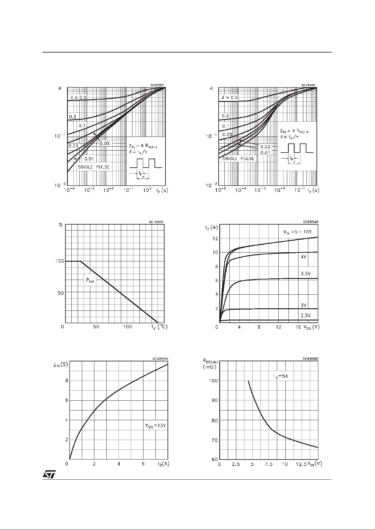
Thermal ImpedanceFor ISOWATT220
Derating Curve
Transconductance
ThermalImpedanceFor D2PAK / PowerSO-10
OutputCharacteristics
StaticDrain-SourceOnResistancevs Input
Voltage
VNB10N07-VNK10N07FM-VNP10N07FI-VNV10N07
5/14
Page 6
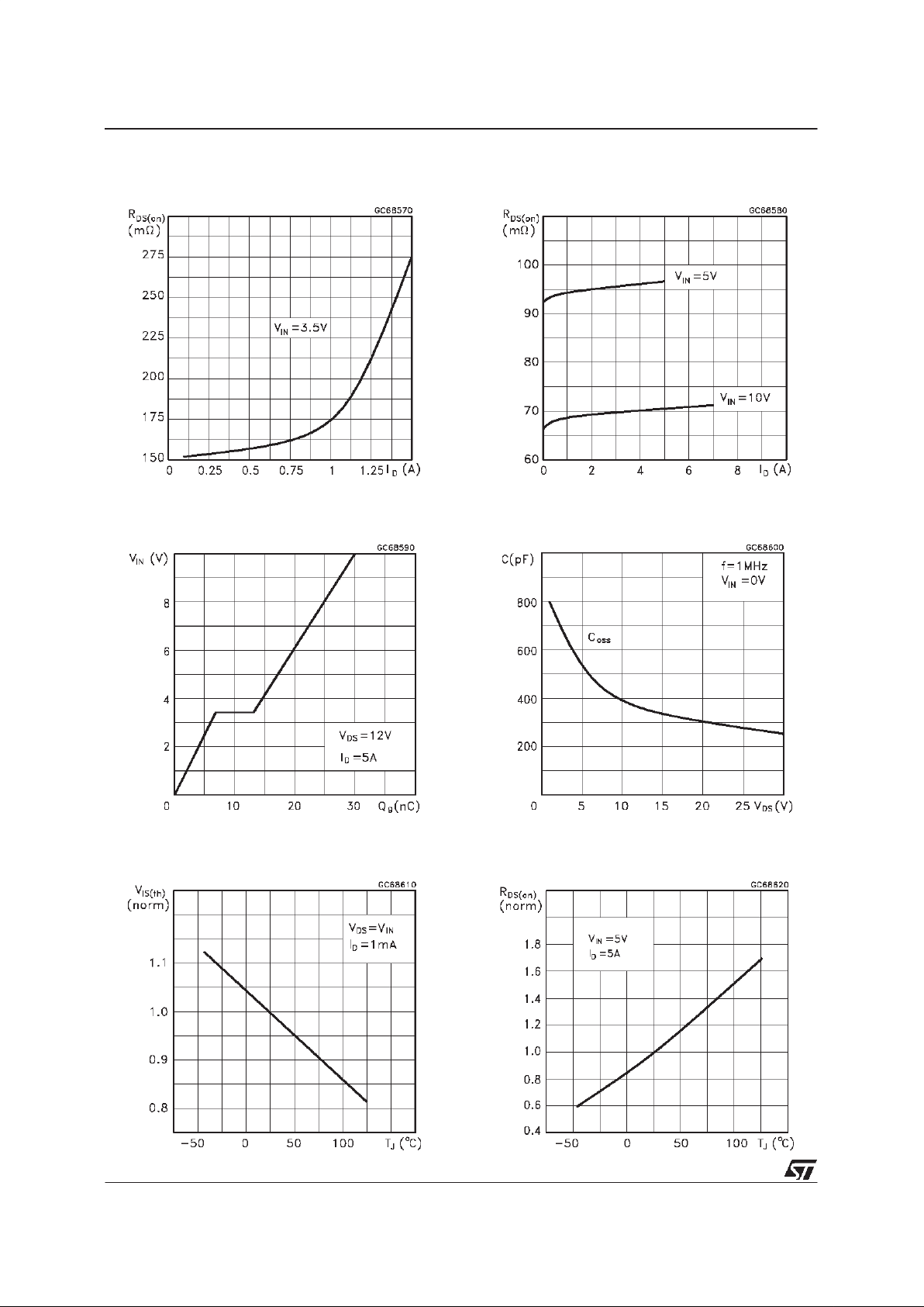
StaticDrain-Source On Resistance
Input Charge vs Input Voltage
Normalized Input Threshold Voltage vs
Temperature
StaticDrain-SourceOnResistance
CapacitanceVariations
Normalized On Resistance vs Temperature
VNB10N07-VNK10N07FM-VNP10N07FI-VNV10N07
6/14
Page 7
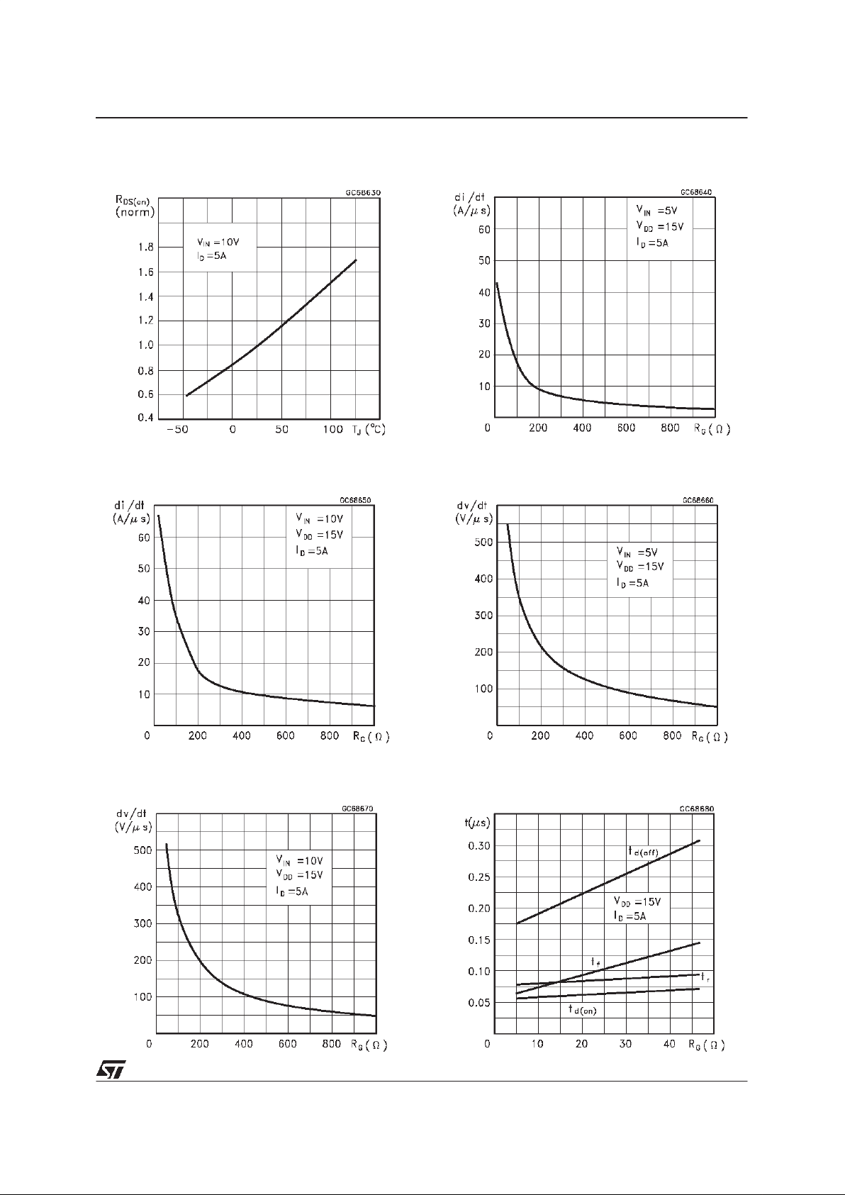
Normalized On Resistance vs Temperature
Turn-onCurrent Slope
Turn-offDrain-Source Voltage Slope
Turn-onCurrent Slope
Turn-off Drain-SourceVoltageSlope
SwitchingTime ResistiveLoad
VNB10N07-VNK10N07FM-VNP10N07FI-VNV10N07
7/14
Page 8
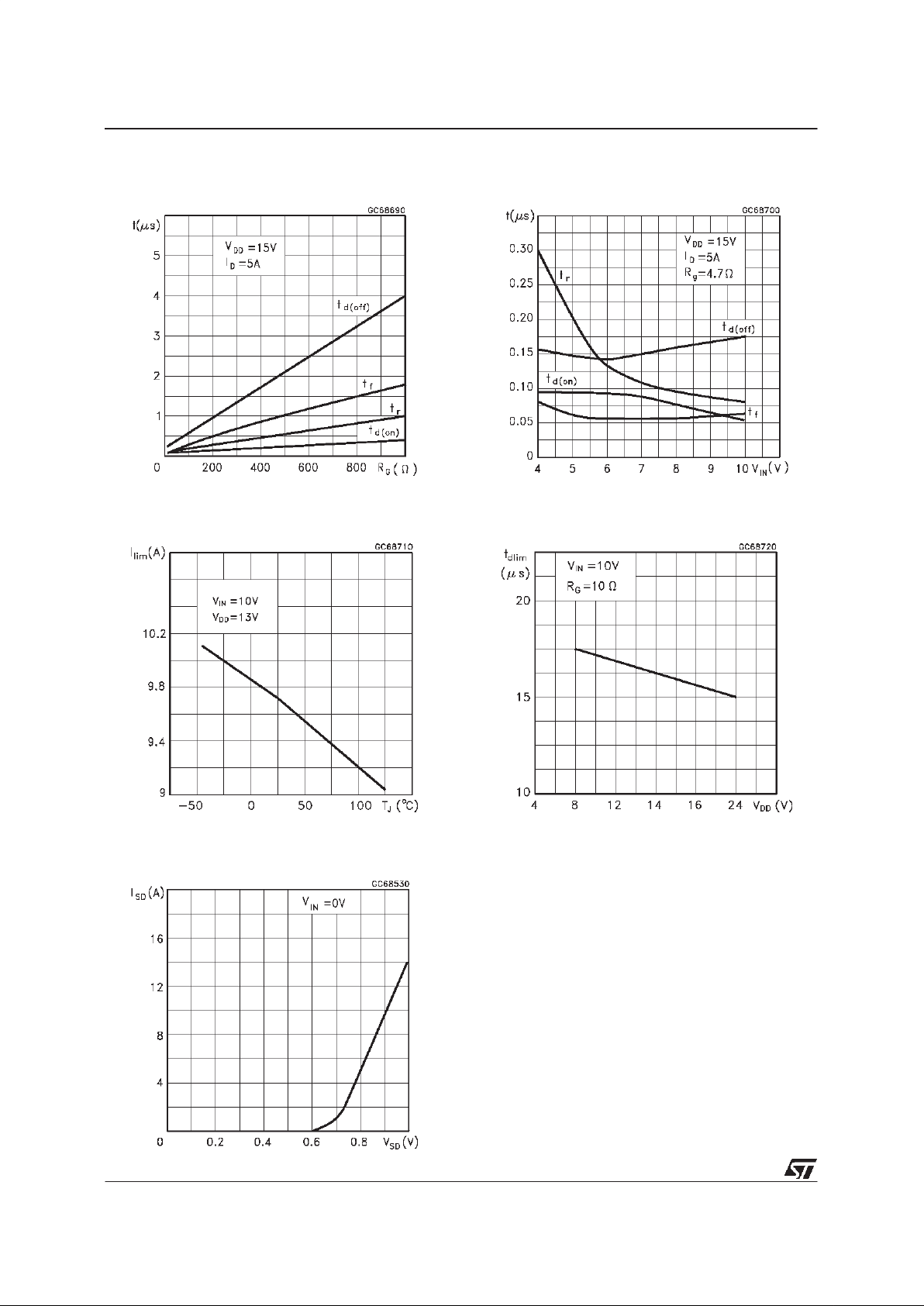
SwitchingTime ResistiveLoad
CurrentLimit vs JunctionTemperature
SourceDrain Diode Forward Characteristics
SwitchingTime ResistiveLoad
Step ResponseCurrent Limit
VNB10N07-VNK10N07FM-VNP10N07FI-VNV10N07
8/14
Page 9
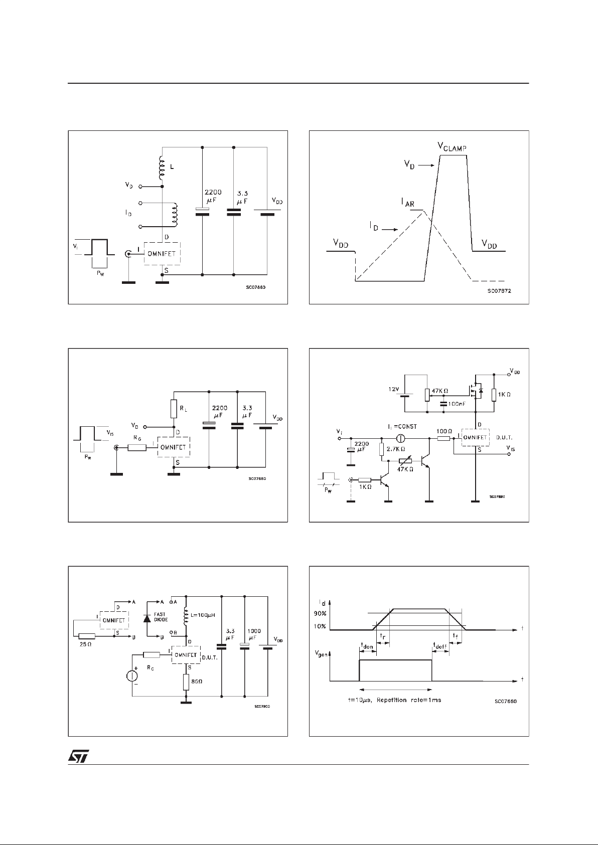
Fig. 2: UnclampedInductiveWaveforms
Fig. 3: SwitchingTimesTest Circuits For
ResistiveLoad
Fig. 4: InputCharge TestCircuit
Fig. 1: Unclamped Inductive Load Test Circuits
Fig. 5: TestCircuit For Inductive Load Switching
And Diode Recovery Times
Fig. 6: Waveforms
VNB10N07-VNK10N07FM-VNP10N07FI-VNV10N07
9/14
Page 10
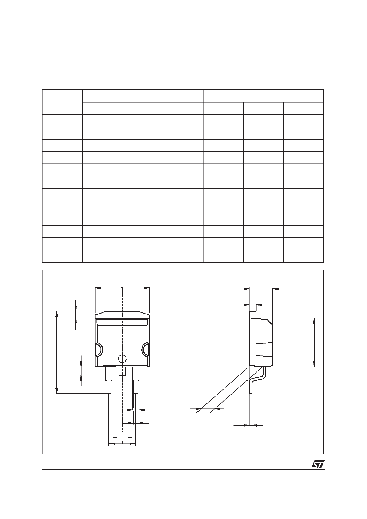
DIM.
mm inch
MIN. TYP. MAX. MIN. TYP. MAX.
A 4.3 4.6 0.169 0.181
A1 2.49 2.69 0.098 0.106
B 0.7 0.93 0.027 0.036
B2 1.25 1.4 0.049 0.055
C 0.45 0.6 0.017 0.023
C2 1.21 1.36 0.047 0.053
D 8.95 9.35 0.352 0.368
E 10 10.28 0.393 0.404
G 4.88 5.28 0.192 0.208
L 15 15.85 0.590 0.624
L2 1.27 1.4 0.050 0.055
L3 1.4 1.75 0.055 0.068
L2
L3
L
B2
B
G
E
A
C2
D
C
A1
P011P6/C
TO-263 (D2PAK) MECHANICAL DATA
VNB10N07-VNK10N07FM-VNP10N07FI-VNV10N07
10/14
Page 11
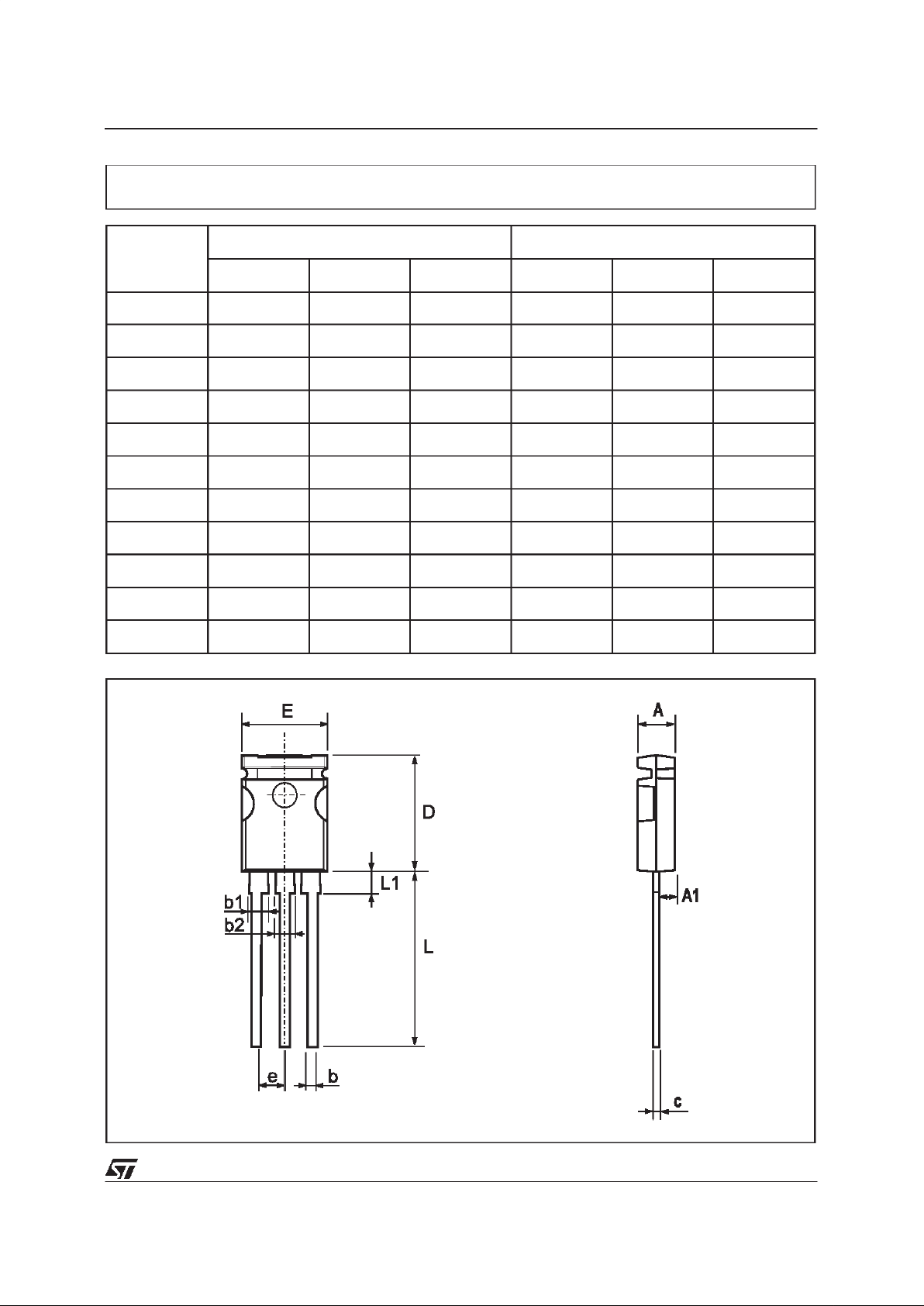
DIM.
mm inch
MIN. TYP. MAX. MIN. TYP. MAX.
A 2.85 3.05 1.122 1.200
A1 1.47 1.67 0.578 0.657
b 0.40 0.60 0.157 0.236
b1 1.4 1.6 0.551 0.630
b2 1.3 1.5 0.511 0.590
c 0.45 0.6 0.177 0.236
D 10.5 10.9 4.133 4.291
e 2.2 2.8 0.866 1.102
E 7.45 7.75 2.933 3.051
L 15.5 15.9 6.102 6.260
L1 1.95 2.35 0.767 0.925
P032R
SOT82-FM MECHANICAL DATA
VNB10N07-VNK10N07FM-VNP10N07FI-VNV10N07
11/14
Page 12
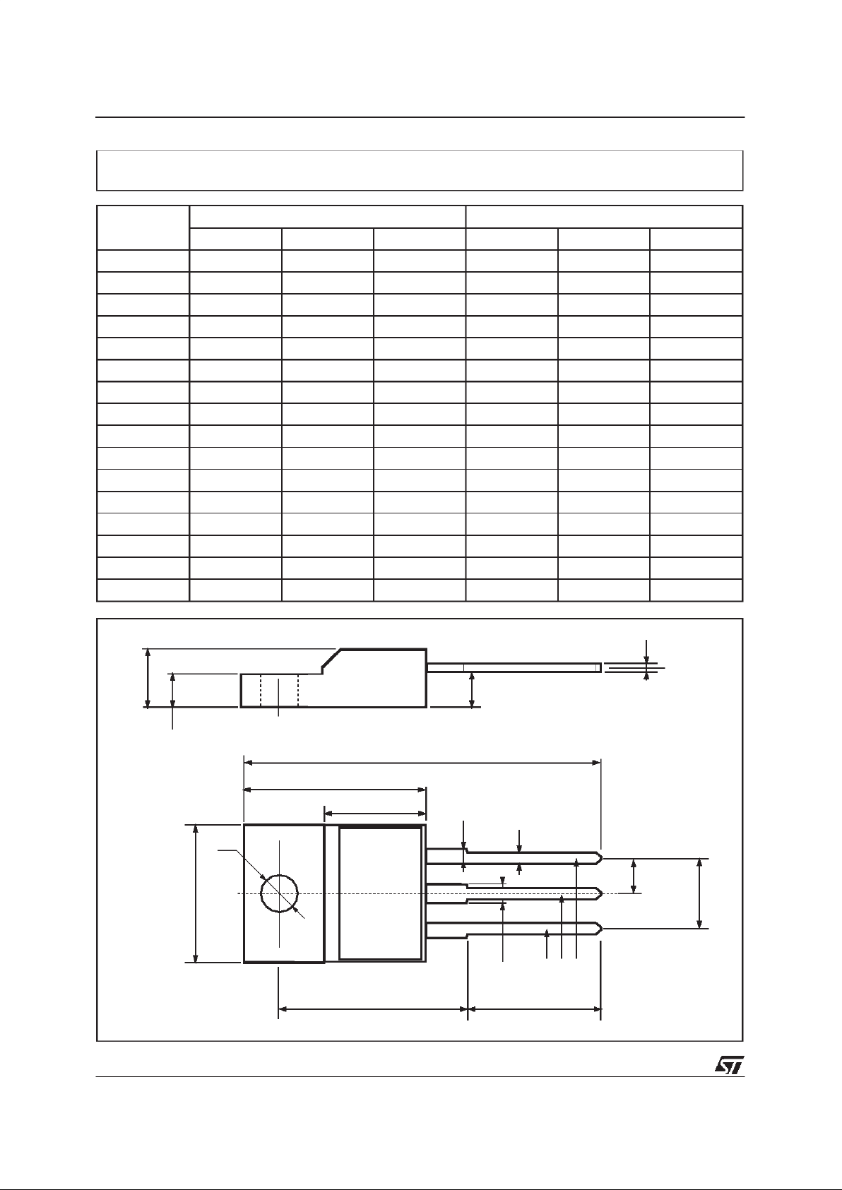
DIM.
mm inch
MIN. TYP. MAX. MIN. TYP. MAX.
A 4.4 4.6 0.173 0.181
B 2.5 2.7 0.098 0.106
D 2.5 2.75 0.098 0.108
E 0.4 0.7 0.015 0.027
F 0.75 1 0.030 0.039
F1 1.15 1.7 0.045 0.067
F2 1.15 1.7 0.045 0.067
G 4.95 5.2 0.195 0.204
G1 2.4 2.7 0.094 0.106
H 10 10.4 0.393 0.409
L2 16 0.630
L3 28.6 30.6 1.126 1.204
L4 9.8 10.6 0.385 0.417
L6 15.9 16.4 0.626 0.645
L7 9 9.3 0.354 0.366
Ø 3 3.2 0.118 0.126
L2
A
B
D
E
H
G
L6
¯
F
L3
G1
123
F2
F1
L7
L4
ISOWATT220MECHANICAL DATA
P011G
VNB10N07-VNK10N07FM-VNP10N07FI-VNV10N07
12/14
Page 13

DIM.
mm inch
MIN. TYP. MAX. MIN. TYP. MAX.
A 3.35 3.65 0.132 0.144
A1 0.00 0.10 0.000 0.004
B 0.40 0.60 0.016 0.024
c 0.35 0.55 0.013 0.022
D 9.40 9.60 0.370 0.378
D1 7.40 7.60 0.291 0.300
E 9.30 9.50 0.366 0.374
E1 7.20 7.40 0.283 0.291
E2 7.20 7.60 0.283 0.300
E3 6.10 6.35 0.240 0.250
E4 5.90 6.10 0.232 0.240
e 1.27 0.050
F 1.25 1.35 0.049 0.053
H 13.80 14.40 0.543 0.567
h 0.50 0.002
L 1.20 1.80 0.047 0.071
q 1.70 0.067
α 0
o
8
o
DETAIL”A”
PLANE
SEATING
α
L
A1
F
A1
h
A
D
D1
==
==
==
E4
0.10 A
E1E3
C
Q
A
==
B
B
DETAIL”A”
SEATING
PLANE
==
==
E2
610
51
eB
HE
M
0.25
==
==
0068039-C
PowerSO-10MECHANICAL DATA
VNB10N07-VNK10N07FM-VNP10N07FI-VNV10N07
13/14
Page 14

Information furnished is believed tobe accurate and reliable.However, STMicroelectronics assumes no responsibility for theconsequences
of use of such information nor for any infringement of patents or other rights of third parties which may result from its use. No license is
granted by implication orotherwise under any patent or patent rights of STMicroelectronics. Specification mentioned in this publication are
subject tochangewithoutnotice. This publication supersedesandreplaces all informationpreviously supplied. STMicroelectronics products
are not authorized for use as critical componentsin life support devices or systems withoutexpress written approval of STMicroelectronics.
The ST logo isa trademarkof STMicroelectronics
1998 STMicroelectronics– Printedin Italy– All Rights Reserved
STMicroelectronicsGROUP OF COMPANIES
Australia -Brazil - Canada- China - France - Germany- Italy- Japan- Korea - Malaysia - Malta- Mexico- Morocco - TheNetherlands -
Singapore- Spain- Sweden- Switzerland- Taiwan -Thailand - United Kingdom- U.S.A.
.
VNB10N07-VNK10N07FM-VNP10N07FI-VNV10N07
14/14
 Loading...