

Page 1
VN771P
QUAD SMART POWER SOLID STATE RELAY
FOR COMPLETE H BRIDGE CONFIGURATIONS
September 1998
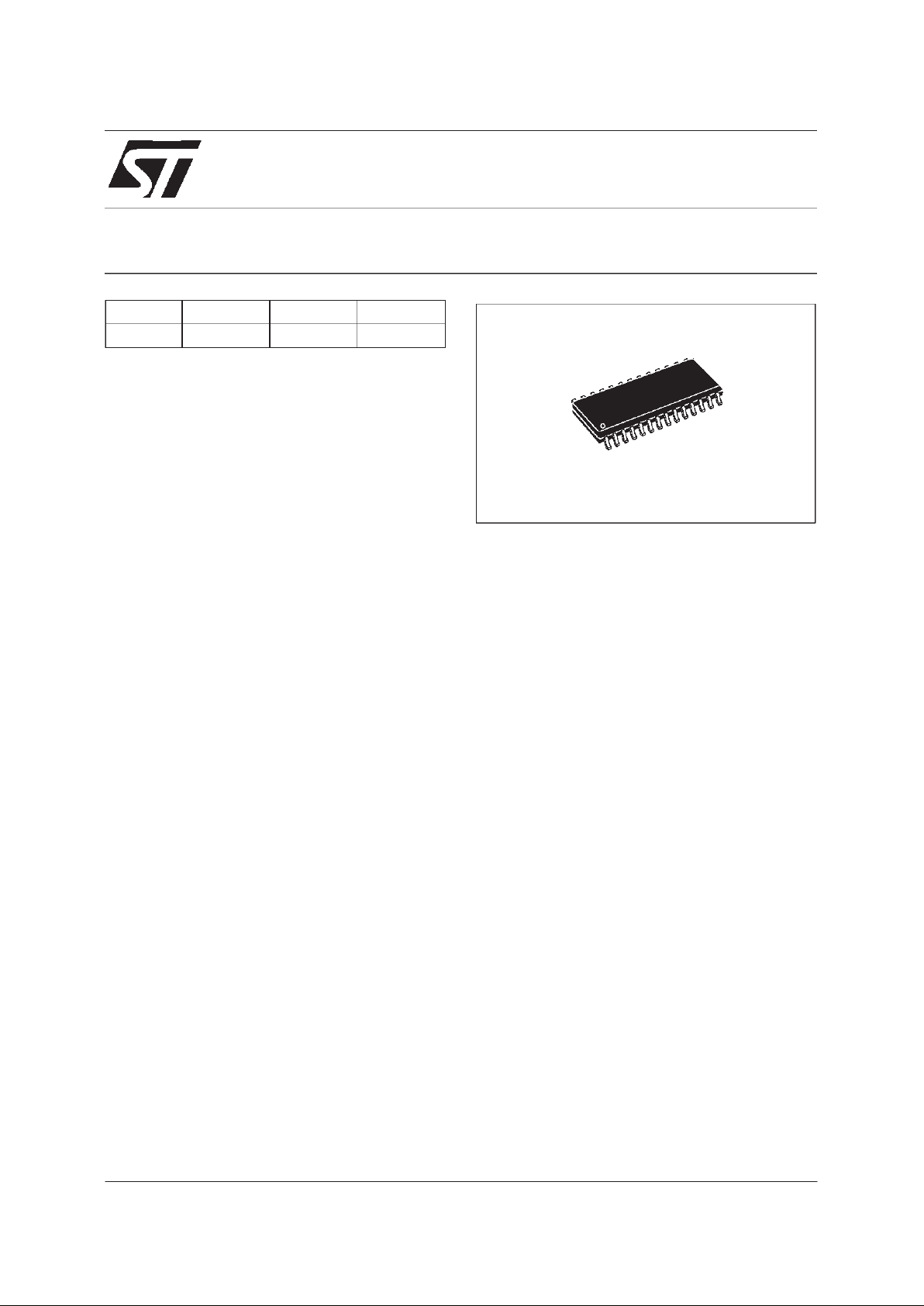
SO-28
TYPE R
DS(on)
*I
OUT
V
CC
VN77 1P 0.135 Ω 14 A 26 V
* Total resistanceof one side in bridge configuration
■ SUITED ASLOWVOLTAGEBRIDGE
■ LINEARCURRENT LIMITATION
■ VERYLOW STAND-BY POWER
DISSIPATION
■ SHORTCIRCUIT PROTECTED
■ STATUSFLAG DIAGNOSTICS
■ OPENDRAIN DIAGNOSTICSOUTPUT
■ INTEGRATEDCLAMPINGCIRCUITS
■ UNDER-VOLTAGEPROTECTION
■ ESDPROTECTION
DESCRIPTION
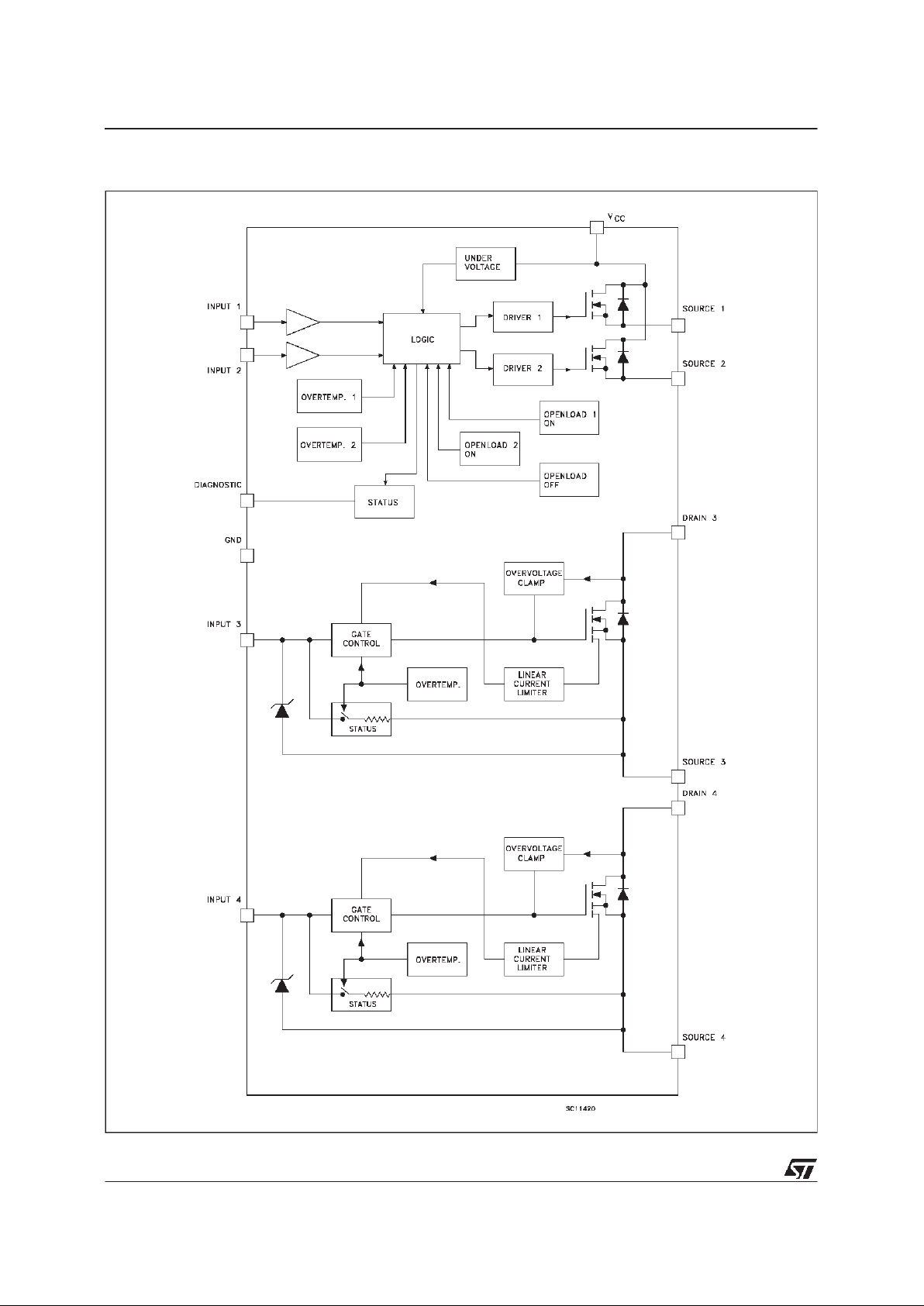
The VN771P is a device formed by three
monolithic chips housed in a standard SO28
package: a double high side and two low side
switches. Both the double high side and low side
switches are made using STMicroelectronics
VIPower technology. This device is suitable to
drive a DC motor in a bridge configurationas well
as to be used as a quad switch for any low
voltage application. The dual high side switches
have built-in thermal shut-down to protect the
chip from over temperature and short circuit,
status output to provide indication for open load
in off and on state, overtemperature conditions
and stuck-on to V
CC
. The low side switches are
two OMNIFET types (fully autoprotected Power
MOSFET in VIPower technology). They have
built-in thermalshut-down, linear current limitation
and overvoltage clamping. Fault feedback for
thermal intervention can be detected by
monitoringthe voltage at the input pin.
DUALHIGH-SIDE SWITCH
From the falling edge of the input signal, the
status output, initially low to signal a fault
condition (overtemperature or open load
on-state), will go back to a high state with a
different delay in case of overtemperature(tpovl)
and in case of open open load (
tpol
) respectively.
This feature allows to discriminate the nature of
the detected fault. To protect the device against
short circuit and over current condition, the
thermal protection turns the integrated Power
MOS off at a minimum junction temperature of
140
o
C. When this temperature returns to 125oC
the switch is automatically turned on again. In
short circuit the protectionreacts with virtually no
delay, the sensor (one for each channel) being
locatedinside each of the two Power MOS areas.
This positioning allows the device to operate with
one channelin automaticthermal cycling and the
other one on a normal load. An internal function
of the devices ensures the fast demagnetization
of inductive loads with a typical voltage (V
demag
)
of -18V. This function allows to greatly reduces
the power dissipationaccording to the formula:
P
dem
=0.5• L
load
• (I
load
)2• [(VCC+V
demag
)/V
demag
] • f
wheref = switching frequencyand
V
demag
= demagnetizationvoltage.
In this device if the GND pin is disconnected,with
V
CC
not exceeding 16V, both channel will switch
off.
LOW-SIDESWITCHES
During normal operation, the Input pin is
electrically connected to the gate of the internal
power MOSFET. The device then behaves like a
standard power MOSFET and can be used as a
switch from DC to 50 KHz. The only difference
from the user’s standpoint is that a small DC
current (I
iss
) flows into the Input pin in order to
supplythe internalcircuitry.
1/11
Page 2
BLOCK DIAGRAM
VN771P
2/11
Page 3
CONNECTION DIAGRAM
PIN FUNCTION
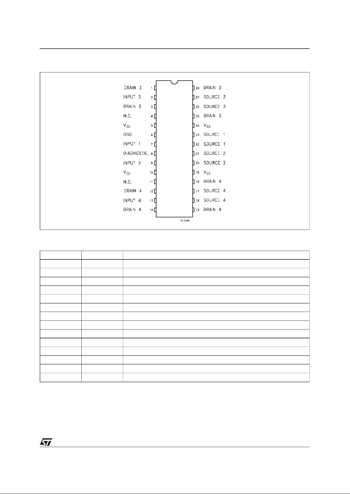
No NAME FUNCTI O N
1, 3, 25, 28 DRAI N 3 Drain of S wit c h 3 (low -s ide switch)
2 INP UT 3 I nput of Switch 3 (low-side switch)
4, 11 N.C. Not Connected
5, 10, 19, 2 4 V
CC
Drain of S wit c h es 1and 2 (high- side s wit ches) and Power S upply Volt age
6 GND Grou nd of Switches 1 and 2 (high -s ide switches)
7 INP UT 1 I nput of Switch 1 (high-side s wit c h )
8 DIAGNO S T IC Diagn os tic of Switc hes 1 and 2 (h igh-side switches )
9 INP UT 2 I nput of Switch 2 (high-side s wit c h )
12, 14, 15, 1 8 DRAIN 4 Drain of S witc h 4 (low-side switch)
13 INP UT 4 I nput of Switch 4 (low-side switch)
16, 17 SO URC E 4 Source of S w it ch 4 (low-side switch)
20, 21 SO URC E 2 Source of S w it ch 2 (high- s ide s wit ch)
22, 23 SO URC E 1 Source of S w it ch 1 (high- s ide s wit ch)
26, 27 SO URC E 3 Source of S w it ch 3 (low-side switch)
VN771P
3/11
Page 4
PROTECTION CIRCUITS
DUALHIGH SIDESWITCH
The simplest way to protect the device against a
continuous reverse battery voltage (-26V) is to
insert a a small resistor betweenpin 2 (GND) and
ground. The suggested resistance value is about
150Ω. In any case the maximum voltage drop on
this resistorshould not overcome0.5V.
If there is no need for the control unit to handle
external analog signals referred to the power
GND, the best approach is to connect the
reference potential of the control unit to the
device ground (see application circuit in fig. 3),
which becomes the common signal GND for the
whole control board avoiding shift of V
ih,Vil
and
V
stat
.
LOW SIDESWITCHES
The devices integrate:
- OVERVOLTAGE CLAMP PROTECTION:
internally set at 42V, along with the rugged
avalanche characteristics of the Power
MOSFET stage give this device unrivalled
ruggedness and energy handling capability.
This feature is mainly important when driving
inductive loads.
- OVERTEMPERATUREAND SHORT CIRCUIT
PROTECTION: these are based on sensing
the chiptemperature and are notdependent on
the input voltage. The location of the sensing
element on the chip in the power stage area
ensures fast, accurate detection of the junction
temperature. Overtemperaturecutout occurs at
minimum 150
o
C. The device is automatically
restarted when the chip temperature falls
below 135
o
C.
- STATUS FEEDBACK: In the case of an
overtemperature fault condition, a Status
Feedback is provided through the Input pin.
The internal protection circuit disconnects the
input from the gate and connects it instead to
ground via an equivalent resistance of 100 Ω.
The failure can be detected by monitoring the
voltage at the Input pin, which will be close to
ground potential.
Additional features of these devices are ESD
protection according to the Human Body model
and the ability to be driven from a TTL Logic
circuit (with a smallincrease in R
DS(on)
).
TRUTH TABLE (forDual high-sideswitch only)
INP U T 1 INP UT 2 SO URC E 1 SOUR CE 2 DIAGNOSTIC
Normal Operation L
H
L
H
L
H
H
L
L
H
L
H
L
H
H
L
H
H
H
H
Under-voltage X X L L H
Ther mal Shut dow n
Channel 1
HXLX L
Channel 2
XHXL L
Open Load
Channel 1
H
L
X
L
H
L
X
L
L
L
Channel 2
X
L
H
L
X
L
H
L
L
L
Out put Short ed t o V
CC
Channel 1
H
L
X
L
H
H
X
L
L
L
Channel 2
X
L
H
L
X
L
H
H
L
L
NOTE: The low-side switches have the fault feedback which can be detected by monitoringthe voltage at the input pins.
L = Logic LOW, H = Logic HIGH, X = Don’t care
VN771P
4/11
Page 5
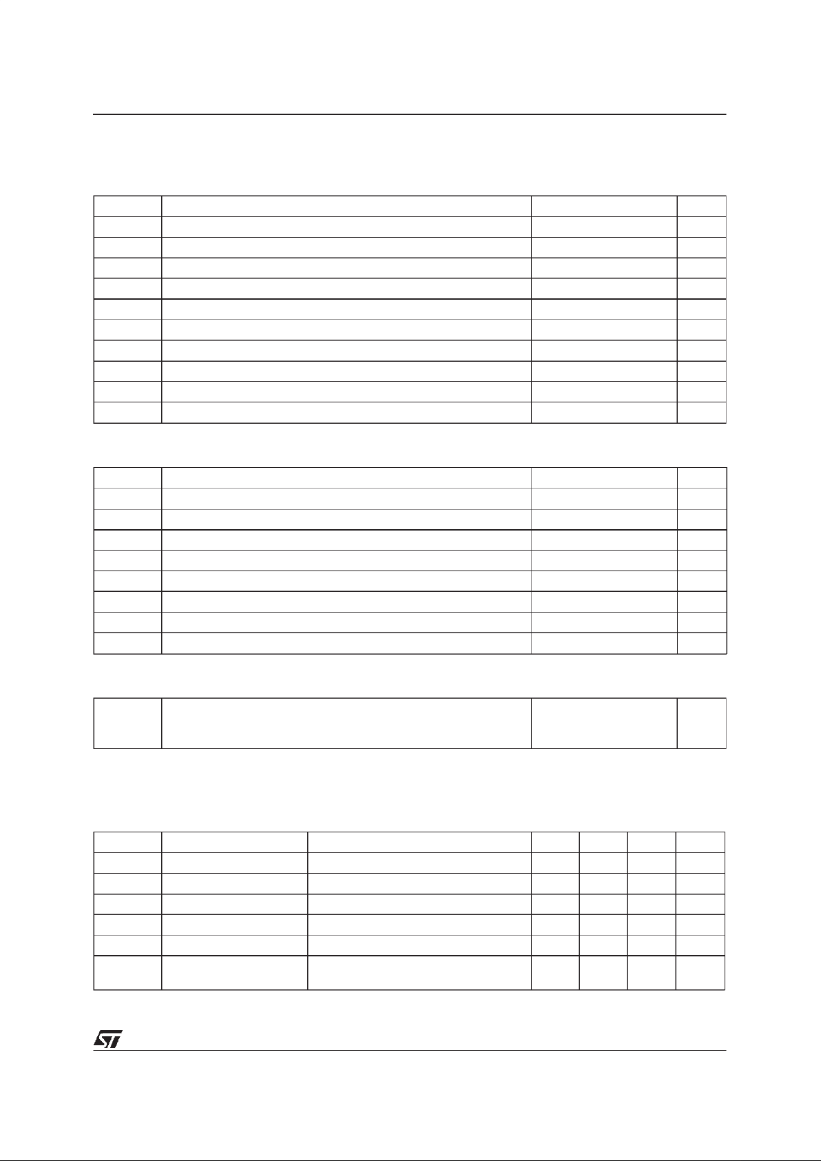
ABSOLUTE MAXIMUMRATING (-40oC<Tj<150oC)
HIGHSIDE SWITCH
Symbol Parameter Value Unit
V
(BR)DSS
Drain-So urc e B reakdow n Voltag e 40 V
I
OUT
Outpu t Current (cont . ) 14 A
I
R
Revers e Out put Cur re nt -14 A
I
IN
Input Current ±10 mA
-V
CC
Revers e Supply Voltage -4 V
I
STAT
Status Current ±10 m A
V
ESD
Elect ro st a t ic Dischar ge (C = 100 pF , R =1. 5 KΩ) 2000 V
P
tot
Power Dissipation at Tc=25oC Inte r nally Limit ed W
T
j
Junct ion Operating T emperature -40 to 150
o
C
T
stg
Stora ge Tem perat ure -55 to 150
o
C
LOW SIDESWITCH
Symb o l Param et er Val u e Unit
V
(BR)DSS
Drain-So urce Bre akdown Vo lt a ge Int er na lly Clamped V
V
IN
Input Voltage 18 V
I
D
Drain Current Int er nally Lim it ed A
I
R
Revers e DC Out put Cur r ent -28 A
V
ESD
Elect r ost a t ic Disc harge (C = 100 pF, R =1. 5 K Ω)2000V
P
tot
Tot al Diss ipa ti on at Tc=25oC I nternally Limited W
T
j
Operating Junct io n T e m pe ra t ure Int er nally Lim it ed
o
C
T
stg
Stora ge Tem perat ure -55 to 150
o
C
THERMAL DATA
R
thj-case
R
thj-case
R
thj-amb
Thermal Resistan ce Junction-case (High-side switch) Max
Therma l Resistance Jun c t ion -c as e (Low -s ide switc h) Max
Therma l Resistance Jun c t ion -am bient Max
20
20
60
o
C/W
o
C/W
o
C/W
ELECTRICAL CHARACTERISTICS FOR DUALHIGH SIDE SWITCH
(8 < V
CC
< 16 V;-40 ≤ Tj≤ 125oC unless otherwise specified)
POWER
Symb o l Parameter Test Cond iti ons Min. Typ . Max. Unit
V
CC
Supply Voltage 6 13 26 V
In(*) Nominal C urrent T
c
=85oCV
DS(on)
≤ 0. 5 VCC=13V 3.4 5.2 A
R
on
On Stat e Res ist a nc e I
OUT=InVCC
=13V Tj=25oC0.065 0.1Ω
I
S
Supply Current Off St at e Tj=25oCVCC= 13 V 35 100 µA
V
DS(MAX)
Maxim um Volt age Drop I
OUT
=13A Tj=85oCVCC=13V 1.2 2 V
R
i
Outpu t t o G N D internal
Impeda nce
Tj=25oC51020KΩ
VN771P
5/11
Page 6
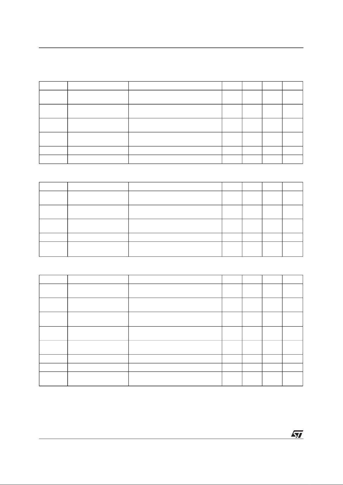
SWITCHING
Symb o l Parameter Test Cond iti ons Min. Typ . Max. Unit
t
d(on)
(^) Turn-on Delay Time Of
Outpu t Current
R
out
=2.7Ω 535200µs
t
r
(^) Rise T ime Of Out put
Current
R
out
=2.7Ω 28 110 360 µs
t
d(off)
(^) Turn-of f Delay Time Of
Outpu t Current
R
out
=2.7Ω 10 140 500 µs
t
f
(^) Fall Ti m e O f Out p ut
Current
R
out
=2.7Ω 28 75 360 µs
(di/dt)
on
Turn-on Current Slope R
out
=2.7Ω 0.003 0.1 A/µ s
(di/dt)
off
Turn-of f Current Slope R
out
=2.7Ω 0.005 0.1 A/µ s
LOGIC INPUT
Symb o l Parameter Test Cond iti ons Min. Typ . Max. Unit
V
IL
Input Low Level
Voltage
1.5 V
V
IH
Input High Level
Voltage
3.5 (•)V
V
I(hyst.)
Input Hys teresi s
Voltage
0.2 0.9 1. 5 V
I
IN
Input Current VIN=5V Tj=25oC30100µA
V
ICL
Input Clamp V olt a ge IIN=10mA
I
IN
=-10mA
56
-0.7
7V
V
PROTECTION AND DIAGNOSTICS
Symb o l Parameter Test Cond iti ons Min. Typ . Max. Unit
V
STAT
Status Volt age Out put
Low
I
ST AT
=1.6mA 0.4 V
V
USD
Under Voltage S hut
Down
3.5 4.5 6 V
V
SCL
Status Clamp Voltage I
ST AT
=10mA
I
ST AT
=-10mA
56
-0.7
7V
V
T
TSD
Therma l Shut- d own
Temper at ur e
140 160 180
o
C
T
SD(hyst.)
Therma l Shut- d own
Hysteresis
50
o
C
T
R
Reset Tempera t ur e 125
o
C
V
OL
Open V olt a ge Lev el Off- Stat e (not e 2) 2.5 4 5 V
I
OL
Open Load Curren t
Level
On-State 0.6 0.9 1. 4 A
ELECTRICAL CHARACTERISTICS FOR DUALHIGH SIDE SWITCH (continued)
VN771P
6/11
Page 7
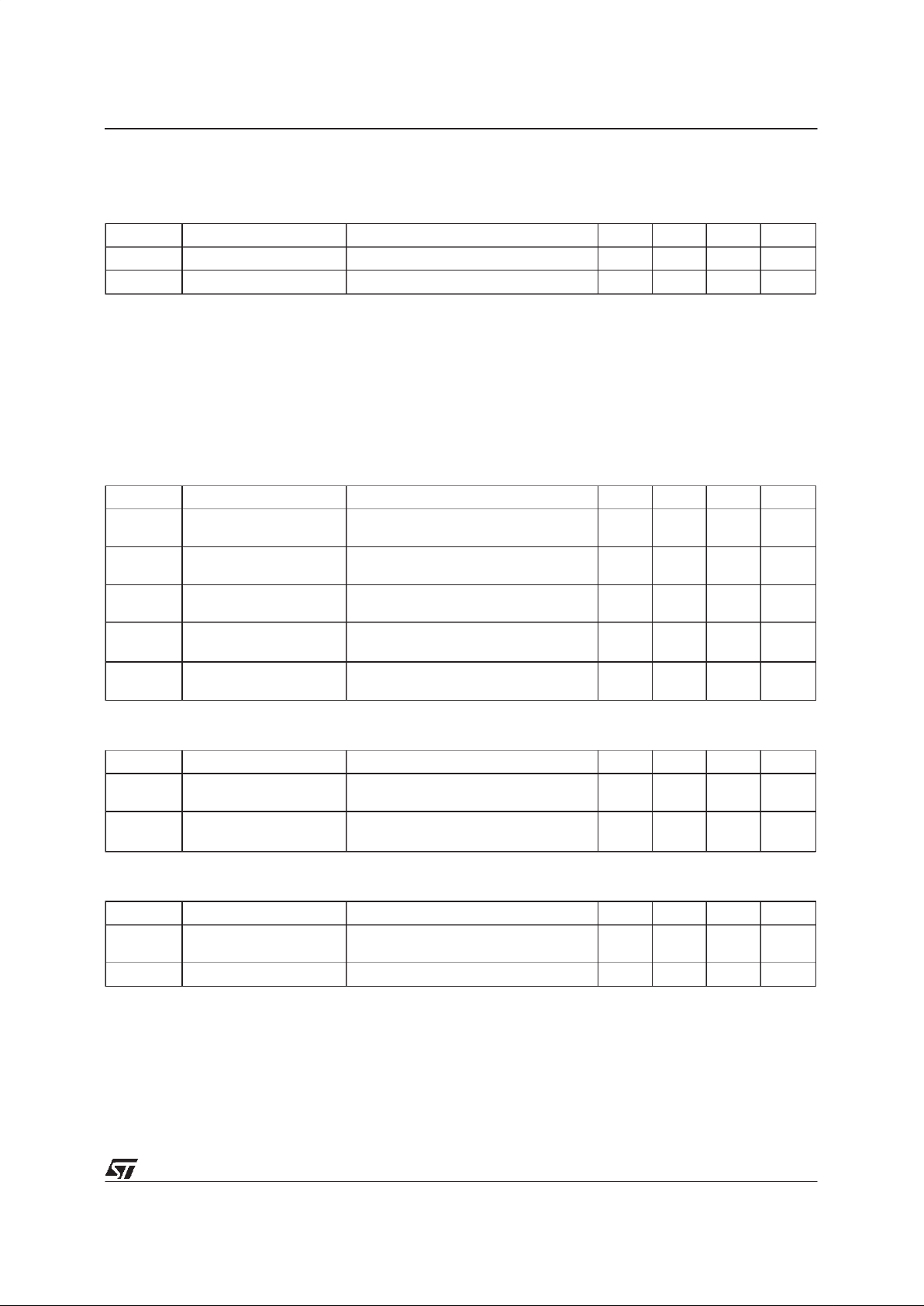
Symb o l Parameter Test Cond iti ons Min. Typ . Max. Unit
t
povl
Statu s Del ay (note 3) 5 10 µs
t
pol
Status Delay (note 3) 50 500 2500 µs
(*) In= Nominal current according to ISO definition for high side automotive switch (see note 1)
(^) See switching time waveform
() The V
IH
is internally clamped at 6V about. Itis possible to connect this pin to an higher voltage via an external resistor calculated to not
exceed 10 mA at the input pin.
note 1: The Nominal Current is the current at T
c
=85oC forbattery voltage of 13V which produces avoltage drop of 0.5 V
note 2: I
OL(off)
=(VCC-VOL)/R
OL
note 3: t
povltpol
: ISO definition
ELECTRICAL CHARACTERISTICS FOR LOW SIDE SWITCHES
(T
case
=25oC unless otherwise specified)
OFF
Symb o l Parameter Test Cond iti ons Min. Typ . Max. Unit
V
CLAM P
Drain-source Clamp
Voltage
ID=10A Vin= 0 36 42 48 V
V
CLTH
Drain-source Clamp
Threshold Voltage
ID=2mA Vin= 0 35 V
V
INCL
Input-Source Rev erse
Clamp Voltage
Iin=-1mA -1 -0.3 V
I
DSS
Zero I nput Voltage
Drain C ur rent (V
in
=0)
V
DS
=13V Vin=0
V
DS
=25V Vin=0
50
200
µA
µA
I
ISS
Supply Current from
Input Pin
VDS=0V Vin=10V 250 500 µA
ON (∗)
Symb o l Parameter Test Cond iti ons Min. Typ . Max. Unit
V
IN(th)
Input T hreshold
Voltage
VDS=VinID+Iin=1mA 0.8 3 V
R
DS(on)
Static Drain-source On
Resist anc e
Vin=10V ID=10A
V
in
=5V ID=10A
0.035
0.05
Ω
Ω
DYNAMIC
Symb o l Parameter Test Cond iti ons Min. Typ . Max. Unit
g
fs
(∗)Forward
Transconduc t ance
VDS=13V ID= 10 A 14 18 S
C
oss
Output Capacitance VDS=13V f=1MHz Vin= 0 700 9 00 pF
ELECTRICAL CHARACTERISTICS FOR DUALHIGH SIDE SWITCH (continued)
PROTECTION AND DIAGNOSTICS
VN771P
7/11
Page 8
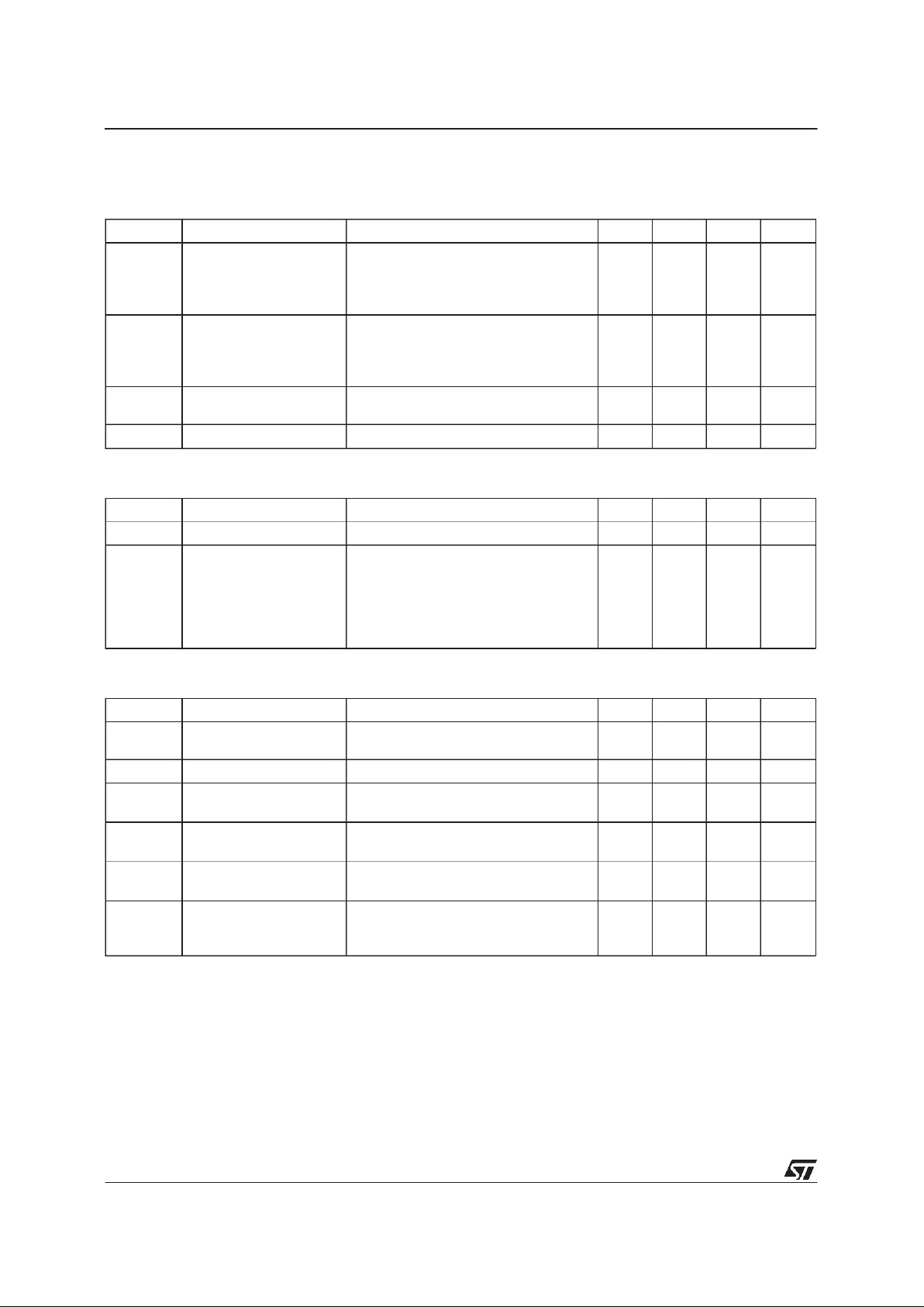
SWITCHING (**)
Symb o l Parameter Test Cond iti ons Min. Typ . Max. Unit
t
d(on)
t
r
t
d(off)
t
f
Turn-on Delay Time
Rise T ime
Turn-off Delay Time
Fall Time
VDD=15V Id=10A
V
gen
=10V R
gen
=10Ω
(see fi gur e 3)
100
330
400
155
200
600
700
300
ns
ns
ns
ns
t
d(on)
t
r
t
d(off)
t
f
Turn-on Delay Time
Rise T ime
Turn-off Delay Time
Fall Time
VDD=15V Id=10A
V
gen
=10V R
gen
= 1000 Ω
(see fi gur e 3)
450
1.7
7.5
3.4
700
3
10
5
ns
µs
µs
µs
(di/dt)
on
Turn-on Current Slope VDD=15V ID=10A
V
in
=10V R
gen
=10Ω
35 A/µs
Q
i
Total I npu t Ch arge VDD=12V ID=10A Vin=10V 60 nC
SOURCEDRAIN DIODE
Symb o l Parameter Test Cond iti ons Min. Typ . Max. Unit
V
SD
(∗) F orward On Voltage ISD=10A Vin=0 1.6 V
t
rr
(∗∗)
Q
rr
(∗∗)
I
RRM
(∗∗)
Revers e Recovery
Time
Revers e Recovery
Charge
Revers e Recovery
Current
I
SD
= 10 A di/dt = 100 A/µs
V
DD
=30V Tj=25oC
(see te s t circuit, figure 5)
180
0.45
7
ns
µC
A
PROTECTION
Symb o l Parameter Test Cond iti ons Min. Typ . Max. Unit
T
jsh
(∗∗) Overt em perature
Shutdown
150
o
C
T
jrs
(∗∗) Ov er tempera t ur e Reset 135
o
C
I
gf
(∗∗) Fault Sink Current Vin=10V VDS=13V
V
in
=5V VDS=13V
50
20
mA
mA
I
lim
Drain C ur rent Limit Vin=10V VDS=13V
V
in
=5V VDS=13V
20
20
28
28
40
40
A
A
t
dlim
(∗∗) St ep R es pon se
Current Limit
Vin=10V
V
in
=5V
25
70
40
120
µs
µs
E
as
(∗∗) Single Pulse A v alance
Energy
starting Tj=25oC
V
in
=10V VDD=20V
R
gen
=1KΩ L=10mH
2.5 J
(∗) Pulsed: Pulse duration = 300 µs, duty cycle 1.5 %
(∗∗) Parametersguaranteed by design/characterization
ELECTRICAL CHARACTERISTICS FOR LOW SIDE SWITCHES (continued)
VN771P
8/11
Page 9
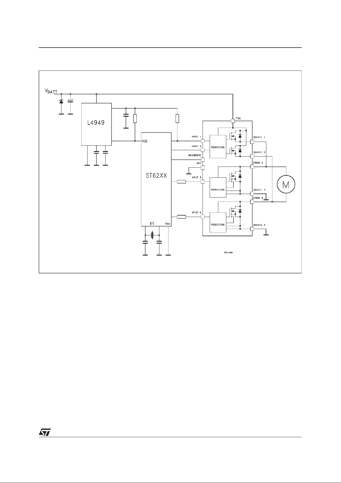
TYPICALAPPLICATIONDIAGRAM
VN771P
9/11
Page 10
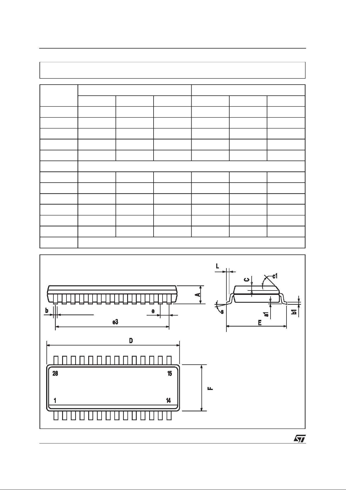
DIM.
mm inch
MIN. TYP. MAX. MIN. TYP. MAX.
A 2.65 0.104
a1 0.10 0.30 0.004 0.012
b 0.35 0.49 0.013 0.019
b1 0.23 0.32 0.009 0.012
C 0.50 0.020
c1 45 (typ.)
D 17.7 18.1 0.697 0.713
E 10.00 10.65 0.393 0.419
e 1.27 0.050
e3 16.51 0.650
F 7.40 7.60 0.291 0.299
L 0.40 1.27 0.016 0.050
S 8 (max.)
0016572
SO-28 MECHANICAL DATA
VN771P
10/11
Page 11

Information furnished is believed to be accurate and reliable. However, STMicroelectronics assumes no responsibility forthe consequences
of use of such information nor for any infringement of patents or other rights of third parties which may result from its use. No license is
granted by implication or otherwise under any patent or patent rights of STMicroelectronics. Specification mentioned in this publication are
subject to change without notice. This publication supersedes and replaces all information previously supplied. STMicroelectronics products
are not authorized for use as critical components inlife support devices or systems without express written approval ofSTMicroelectronics.
The ST logo is a registered trademark of STMicroelectronics
1998 STMicroelectronics –Printed inItaly – All Rights Reserved
STMicroelectronics GROUP OF COMPANIES
Australia - Brazil - Canada - China - France - Germany - Italy - Japan - Korea - Malaysia - Malta - Mexico - Morocco- TheNetherlands -
Singapore - Spain - Sweden - Switzerland - Taiwan - Thailand -United Kingdom - U.S.A.
.
VN771P
11/11
 Loading...