

Page 1
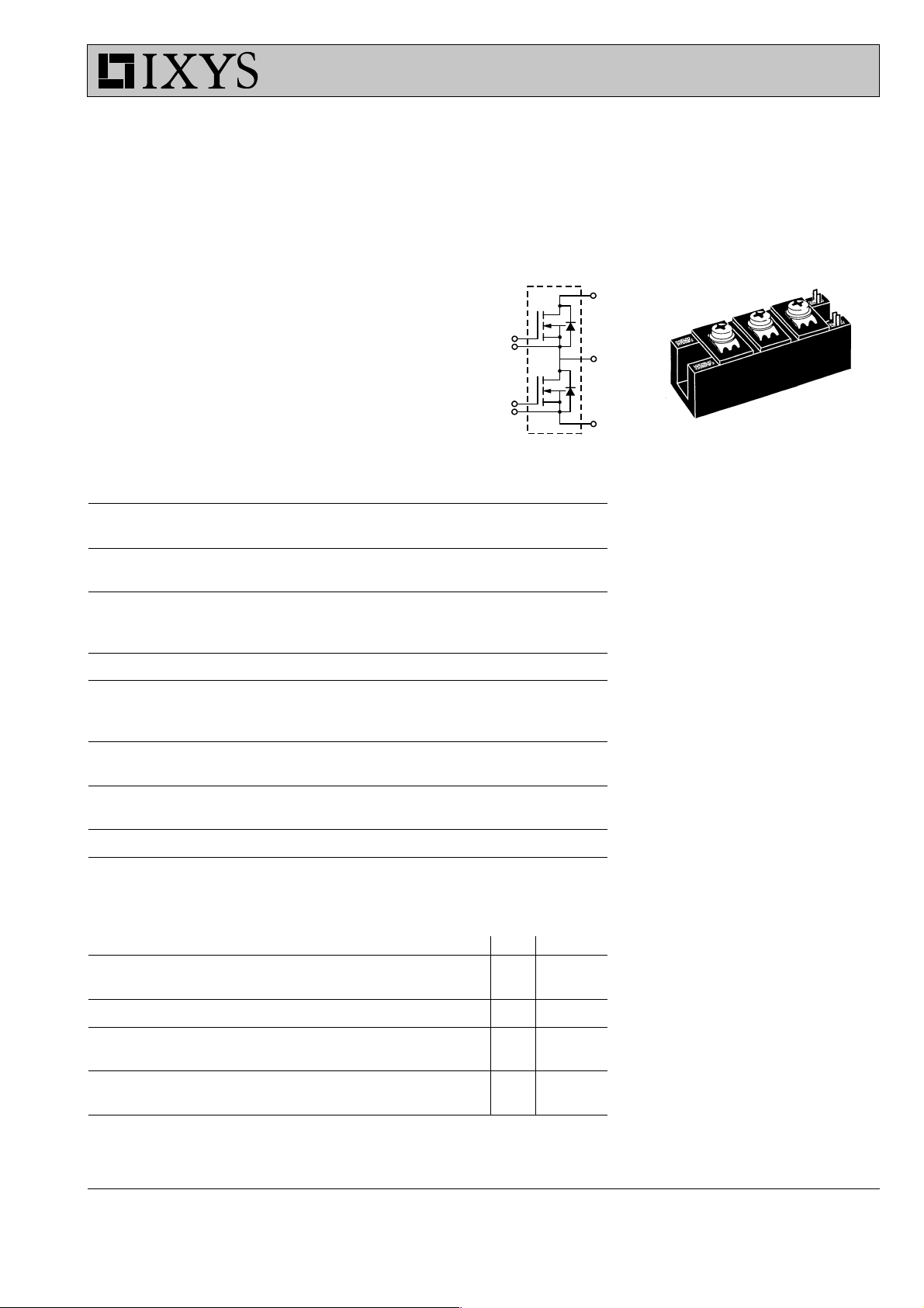
Dual Power
HiPerFET
Phaseleg Configuration
High dv/dt, Low trr, HDMOSTM Family
TM
Module
VMM 85-02F
8
9
11
10
V
DSS
I
D25
R
3
1
2
2 = Source 1 3 = Drain 2
8 = Gate 2 9 = Kelvin Source 2
10 = Kelvin Source 1 11 = Gate 1
DS(on)
= 200 V
= 84 A
= 25 mW
2
1
1 = Drain 1, Source 2
3
11
10
9
8
Symbol Conditions Maximum Ratings
V
DSS
V
DGR
V
GS
V
GSM
I
D25
I
D80
I
DM
P
tot
T
J
T
JM
T
stg
V
ISOL
M
d
TJ= 25°C to 150°C 200 V
TJ= 25°C to 150°C; RGS = 10 kW 200 V
Continuous ±20 V
Transient ±30 V
TC= 25°C 84 A
TC= 80°C 63 A
TC= 25°C, tp = 10 µs, pulse width limited by T
JM
335 A
TC = 25°C 370 W
-40 ... +150 °C
150 °C
-40 ... +125 °C
50/60 Hz t = 1 min 3000 V~
I
£ 1 mA t = 1 s 3600 V~
ISOL
Mounting torque (M5 or 10-32 UNF) 2.25-2.75/20-25 Nm/lb.in.
Terminal connection torque (M5) 2.5-4/22-35 Nm/lb.in.
Weight Typical including screws 130 g
Symbol Conditions Characteristic Values
(TJ = 25°C, unless otherwise specified)
min. typ. max.
Features
• Two MOSFET's in phaseleg config.
• International standard package
• Direct copper bonded Al2O3 ceramic
base plate
• Isolation voltage 3600 V~
• Low R
HDMOSTM process
DS(on)
• Low package inductance for high
speed switching
• Kelvin source contact
Applications
• Switched-mode and resonant-mode
power supplies
• Uninterruptible power supplies (UPS)
Advantages
• Easy to mount with two screws
• Space and weight savings
• High power density
• Low losses
V
V
I
I
R
GSS
DSS
DSS
GS(th)
DS(on)
VGS= 0 V 200 V
VDS= VGS, ID = 8 mA 2 4 V
VGS= ±20 V DC, VDS = 0 500 nA
VDS= V
VDS= 0.8 • V
VGS= 10 V, ID = 0.5 • I
,VGS = 0 V, TJ = 25°C 400 µA
DSS
DSS,VGS
= 0 V, TJ = 125°C 2 mA
D25
Pulse test, t £ 300 µs, duty cycle d £ 2%
Data per MOSFET unless otherwise stated.
IXYS reserves the right to change limits, test conditions and dimensions
© 2000 IXYS All rights reserved
20 25 mW
943
1 - 4
Page 2
VMM 85-02F
Symbol Conditions Characteristic Values
(TJ = 25°C, unless otherwise specified)
min. typ. max.
g
C
C
C
t
d(on)
t
r
t
d(off)
t
f
Q
Q
Q
R
R
d
d
fs
iss
oss
rss
g
gs
gd
thJC
thCH
S
A
VDS= 10 V; ID = 0.5 • I
pulsed 40 6 0 S
D25
9600 15000 pF
VGS = 0 V, VDS = 25 V, f = 1 MHz 1800 4500 pF
620 1500 pF
70 ns
VGS = 10 V, VDS = 0.5 • V
, ID = 0.5 • I
DSS
D25
80 ns
RG = 1 W (External), resistive load 200 ns
100 ns
380 450 nC
VGS = 10 V, VDS = 0.5 • V
, ID = 0.5 • I
DSS
D25
70 110 nC
190 230 nC
0.33K/W
heatsink compound applied 0.2 K/W
Creepage distance on surface 12.7 mm
Strike distance through air 9.6 mm
a Allowable acceleration 50 m/s
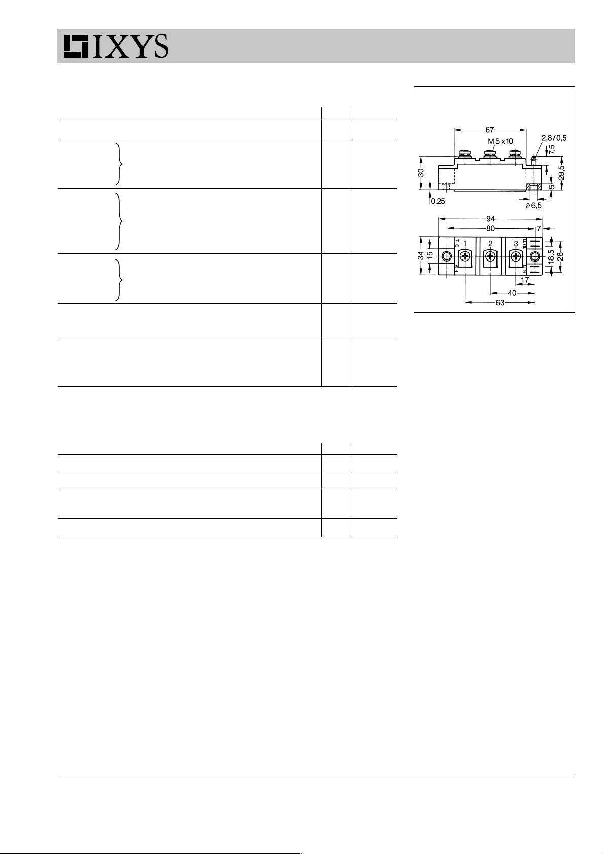
Dimensions in mm (1 mm = 0.0394")
2
Source-Drain Diode Characteristic Values
(TJ = 25°C, unless otherwise specified)
Symbol Conditions min. typ. max.
I
S
I
SM
V
SD
VGS = 0 V 84 A
Repetitive; pulse width limited by T
JM
335 A
IF = IS; VGS = 0 V, 0.9 1.2 V
Pulse test, t £ 300 µs, duty cycle d £ 2%
t
rr
IF = IS, -di/dt = 100 A/µs, VDS = 100 V, VGS = 0 V 200 400 ns
IXYS MOSFETs and IGBTs are covered by one of the following U.S.patents: 4,835,592 4,881,106 5,017,508 5,049,961 5,187,117 5,486,715
© 2000 IXYS All rights reserved
4,850,072 4,931,844 5,034,796 5,063,307 5,237,481 5,381,025
2 - 4
Page 3

VMM 85-02F
I
D
R
DS(on)
norm.
200
A
175
150
VGS = 10 V
9 V
8 V
7 V
125
100
75
6 V
50
25
5 V
0
0123456
V
V
DS
200
VDS = 30 V
A
175
I
D
150
TJ = 25°C
125
100
75
50
25
TJ = 125°C
0
012345678
V
Fig. 1 Typical output characteristics ID = f (VDS) Fig. 2 Typical transfer characteristics ID = f (VGS)
1.4
1.3
normalized to
R
@0.5 I
DS(on)
, VGS = 10V
D25
2.50
R
DS(on)
2.25
norm.
ID = 45 A
2.00
1.2
VGS = 10 V
1.1
1.75
1.50
V
GS
1.0
V
= 15 V
GS
0.9
0.8
0 25 50 75 100 125 150
I
D
Fig. 3 Typical normalized R
= f (ID) Fig. 4 Typical normalized R
DS(on)
100
A
I
80
D
60
40
20
0
0 25 50 75 100 125 150
Fig. 5 Continuous drain current I
= f (TC) Fig. 6 Typical normalized V
D
1.25
1.00
0.75
0.50
A
-50 -25 0 25 50 75 100 125 150
T
J
= f (TJ)
DS(on)
°C
1.2
V
V
GS(th)
V
1.1
DSS
norm.
V
GS(th)
DSS
1.0
0.9
0.8
0.7
°C
T
C
-50 -25 0 25 50 75 100 125 150
= f (TJ), V
DSS
°C
T
J
= f (TJ)
GS(th)
© 2000 IXYS All rights reserved
3 - 4
Page 4

VMM 85-02F
10
V
V
= 100 V
DS
I
= 40 A
D
8
V
I
GS
= 2 mA
G
1000
I
D
A
Limited by R
DS(on)
100
6
4
10
2
0
0 100 200 300 400
nC
Q
g
T
= 25°C
K
T
= 150°C
J
non-repetitive
1
1 10 100 1000
Fig. 7 Typical turn-on gate charge characteristics Fig. 8 Forward Safe Operating Area, ID = f (VDS)
200
A
150
I
S
100
= 125°C
T
J
TJ = 25°C
50
C
100
nF
10
C
iss
C
oss
1
C
rss
t = 1 ms
t = 10 ms
t = 100 ms
V
V
DS
0.1
0 5 10 15 20 25
V
DS
Fig. 9 Typical capacitances C = f (V
), f = 1 MHz Fig. 10 Typical forward characteristics of reverse
DS
100
s
80
g
fs
60
40
20
0
0 20406080100120
I
D
Fig. 11 Typical transconductance g
= f (ID) Fig. 12 Transient thermal resistance Z
fs
0
0
V
0.00 0.25 0.50 0.75 1.00 1.25 1.50
V
V
SD
diode, IS = f (VSD)
1
K/W
D = 0.5
D = 0.2
0.1
thJK
D = 0.1
D=0.05
D=0.02
Z
0.01
D = single pulse
0.001
A
0.001 0.01 0.1 1 10
s
t
= f (tp)
thJK
© 2000 IXYS All rights reserved
4 - 4
 Loading...