

Page 1
D i gital E n t e r t a i n m e n t
ViSTA VES1893
S i n g l e-Chip DSS®/ D V B - S
Continuously Variable Satellite Channel Receiver
O V E R V I E W
The ViSTA VES1893 provides the
ultimate solution for multi-rate systems
targeted at single and dual-mode
DSS®/DVB-S receivers based on VLSI’s
industry leading Integrated Set-Top
Architecture (ViSTA).
The VES1893 builds upon the ViSTA
VES1877 (Dual-mode DSS®/DVBcompliant Satellite Receiver) and the
ViSTA VES1643 (Digital anti-aliasing
programmable low pass filter),
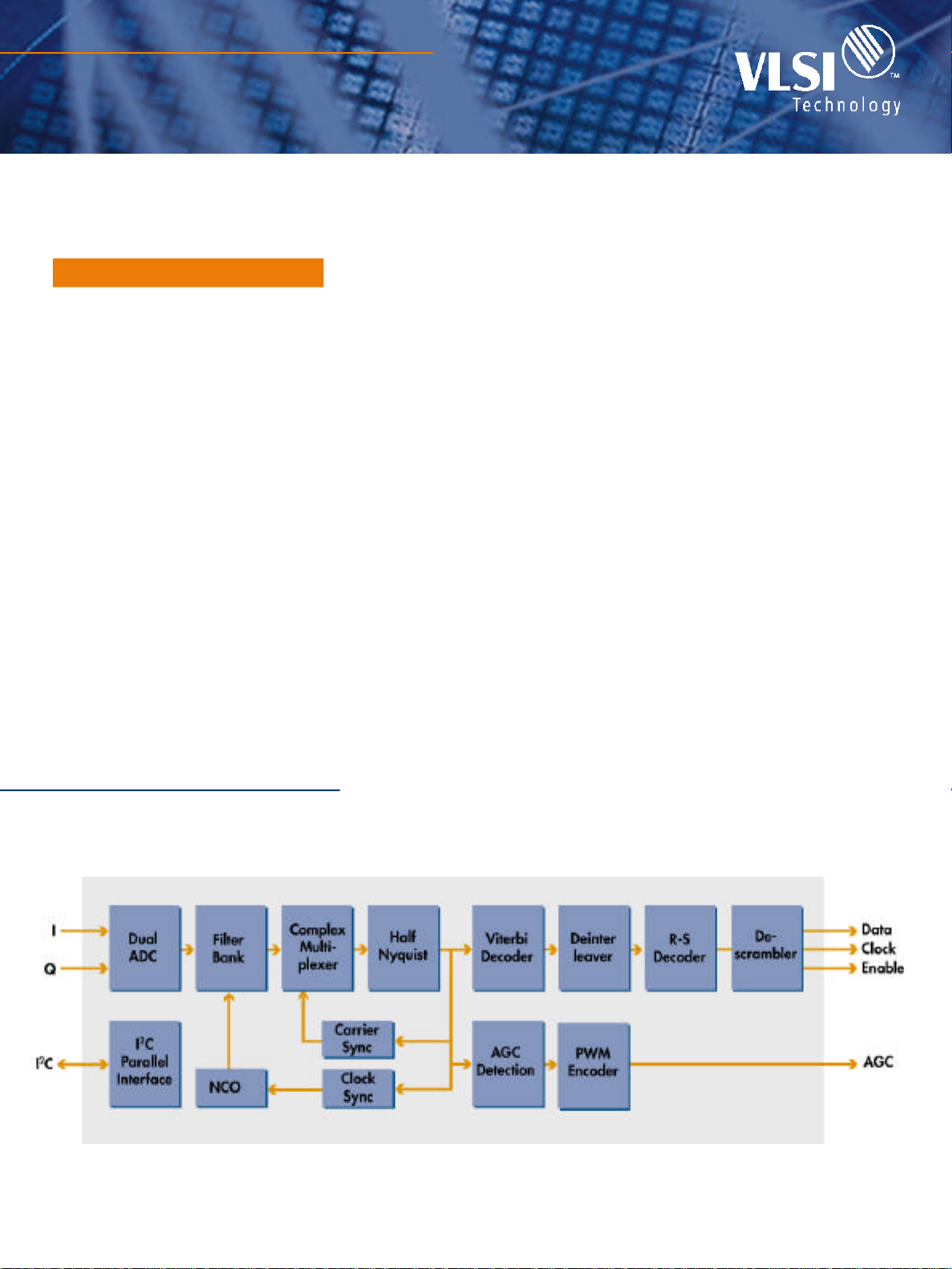
featuring QPSK demodulation, FEC
(Forward Error Correction) functions,
integrated dual analog-to-digital
converters (ADCs), and programmable
anti-aliasing filters.
The integrated universal single chip
satellite channel receiver provides true
variable rate performance between
2 MHz and 90 MHz (1 Mbaud to
45 Mbaud) for both DVB and DSS®. The
device enables continuous system-level
tuning by providing programmable
anti-aliasing filters on-chip. This feature
allows multi-rate applications to tune
from 1 to 45 Mbaud without changing
any components on the system. The
o n - c h i p dual 6-bit Analog-to-Digital
Converters (ADCs) are able to sample
the incoming data at up to 90 MHz.
The VES1893 also provides digital
inputs that bypass the ADCs allowing
for more comprehensive system-level
test and characterization. In bypass
mode, the device interfaces directly
with I and Q digital baseband signals
that are filtered with half-Nyquist
filters. Coherent demodulation is
achieved internally, which negates the
need for an external Voltage Controlled
Crystal Oscillator (VCXO).
The on-chip Forward Error Correction
(FEC) unit decodes two concatenated
codes with the Reed-Solomon used as
the outer code, and a Viterbi decoder
used as the inner code. The ReedSolomon decoder corrects up to 8
erroneous bytes among the N bytes of
one data packet. A embedded deinterleaver with a depth of 12 or 13 blocks
is located between the Viterbi output
and Reed-Solomon decoder input.
B l o c k D i a g r a m
Page 2
A frame synchronization algorithm that
uses timing information from the packet
header automatically synchronizes
the deinterleaver and Reed-Solomon
decoder.
The VES1893 is controlled via an I2C
bus interface. Through this interface
the following DSS®or DVB programmable features are offered: Half-Nyquist
filter; roll-off factor; deinterleaver;
packet length; and Reed-Solomon
decoder.
The device also has the ability to disable the energ y dispersion descrambler,
a feature required for DVB.
F E A T U R E S
• DSS®and DVB-S compatible single
chip demodulation and forward
error correction
• 6-bit dual analog-to-digital
converters (ADCs)
• Variable rate BPSK/QPSK coherent
demodulator
• Modulation rates up to 45 Mbaud
• Analog power estimation for AGC
• Carrier recovery
• Programmable second-order loop
filter.
• AFC output provision
• Acquisition Range up to +/- SR/2
(SR = Symbol Rate)
• Carrier Lock Detection
• On-chip Half-Nyquist baseband filters
• Selectable roll-off factors
• Viterbi decoder:
·Supported rates: from 1/2 to 8/9
· Constraint length K=7 with
G1 = 1718 and G2 = 1338
· Automatic depuncturing and
bit synchronization for all rates
including spectral inversion
resolution
· Coding gain of 5.4 dB at BER
of 10-5, rate of 1/2
· VBER measurements provided
• Reed-Solomon decoder
· Programmable block length
· Fixed power correction of t = 8
• Programmable convolutional
deinterleaving
• Automatic frame synchronization
• I2C Bus interface, for easy control
• 100 MQFP package
• 0.35 µm CMOS technology
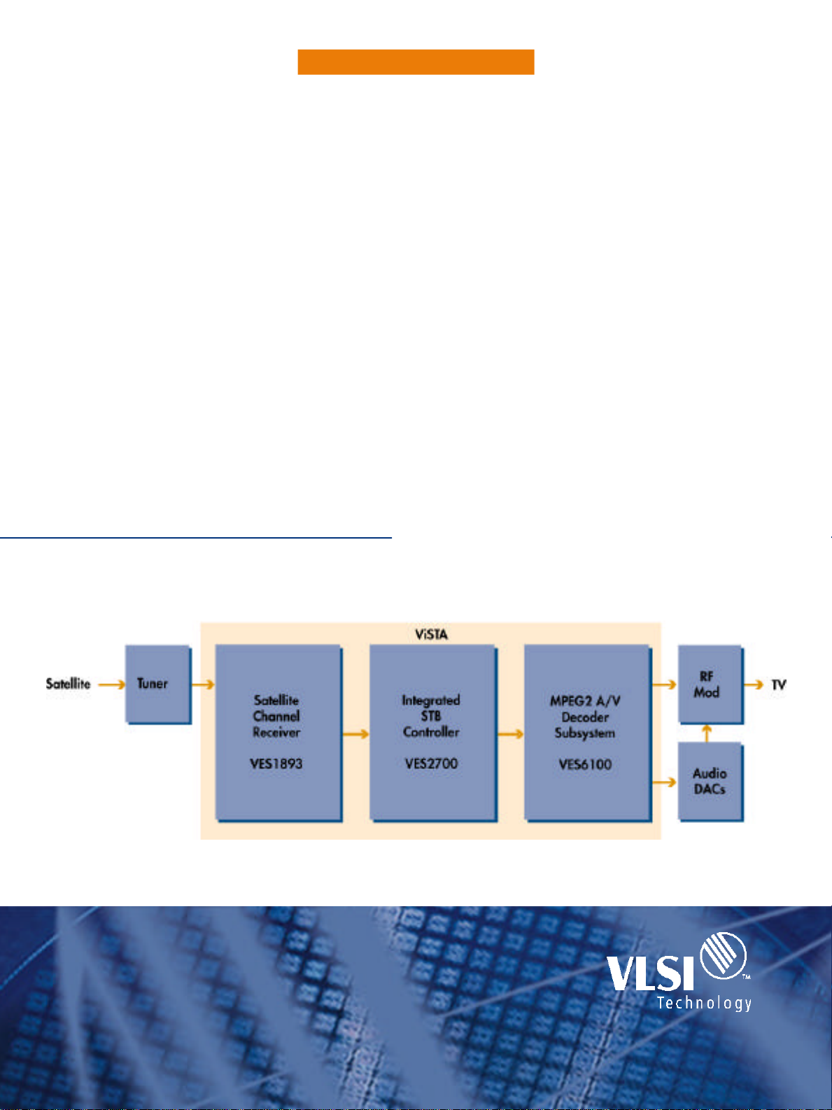
T y p i c a l A p p l i c a t i o n
All brands, product names, and company names are trademarks or registered trademarks of their respective owners.
With respect to the information in this document, VLSI
Technology, Inc. (VLSI) makes no guarantee or warranty of its
accuracy or that the use of such information will not infringe
upon the intellectual rights of third parties. VLSI shall not be
responsible for any loss or damage of whatever nature resulting from the use of, or reliance upon it and no patent or other
license is implied hereby. This document does not in any way
extend or modify VLSI’s warranty on any product beyond that
set forth in its standard terms and conditions of sale. VLSI
reserves the right to make changes in its products and specifications at any time and without notice.
LIFE SUPPORT APPLICATIONS:
V L S I ’s products are not intended for use as critical
components in life support appliances, devices, or systems, in which the failure of a VLSI product to
p e rf o rm could be expected to result in personal injury.
For update information, please visit our Web site:
h t t p : / / w w w. v l s i . c o m
© 1997 VLSI Technology, Inc. Printed in USA
Document Control: PB-V/iSTA-1893 V1.2 December 97
VLSI Technology, Inc.
1109 McKay Drive
San Jose, CA 95131
 Loading...