

Page 1
19225
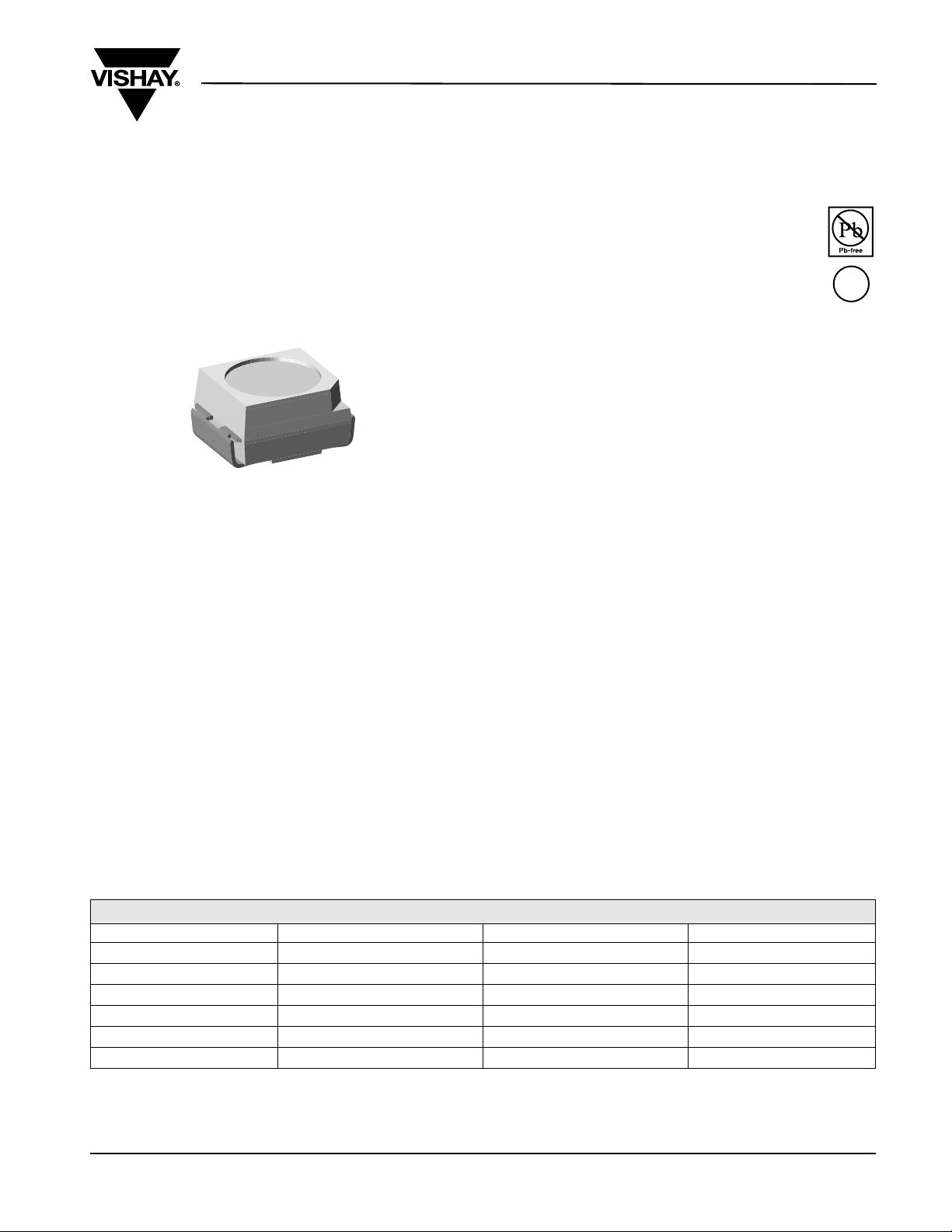
High Intensity SMD LED
FEATURES
• SMD LED with exceptional brightness
• Luminous intensity categorized
• Compatible with automatic placement
equipment
• EIA and ICE standard package
• Compatible with IR Reflow, vapor phase and wave
solder processes according to CECC 00802 and
J-STD-020C
• Available in 8 mm tape
• Low profile package
• Non-diffused lens: excellent for coupling to light
pipes and backlighting
• Low power consumption
• Luminous intensity ratio in one packaging unit
I
Vmax/IVmin
• Lead (Pb)-free device
• Component in accordance to RoHS 2002/95/EC
and WEEE 2002/96/EC
• Preconditioning acc. to JEDEC Level 2a
• ESD-withstand voltage:
up to 2 kV according to JESD22-A114-B
≤ 1.6
VLMS31..
Vishay Semiconductors
e3
DESCRIPTION
The package of the VLMS31.. is the PLCC-2.
It consists of a lead frame which is embedded in a
white thermoplast. The reflector inside this package is
filled up with clear epoxy.
APPLICATIONS
• Automotive: Backlighting in dashboards and
switches
• Telecommunication: Indicator and backlighting in
telephone and fax
• Indicator and backlight for audio and video equipment
• Indicator and backlight in office equipment
• Flat backlight for LCDs, switches and symbols
• General use
PARTS TABLE
PART COLOR, LUMINOUS INTENSITY ANGLE OF HALF INTENSITY (± ϕ) TECHNOLOGY
= (4.5 to 11.2) mcd
VLMS31J1K2-GS08
VLMS31J1K2-GS18
VLMS31J1L2-GS08
VLMS31J1L2-GS18
VLMS31K1L2-GS08
VLMS31K1L2-GS18
Red, I
V
Red, I
= (4.5 to 11.2) mcd
V
Red, I
= (4.5 to 18) mcd
V
Red, I
= (4.5 to 18) mcd
V
Red, I
= (7.1 to 18) mcd
V
Red, I
= (7.1 to 18) mcd
V
60° GaAsP on GaP
60° GaAsP on GaP
60° GaAsP on GaP
60° GaAsP on GaP
60° GaAsP on GaP
60° GaAsP on GaP
Document Number 81327
Rev. 1.0, 17-Oct-06
www.vishay.com
1
Page 2
VLMS31..
Vishay Semiconductors
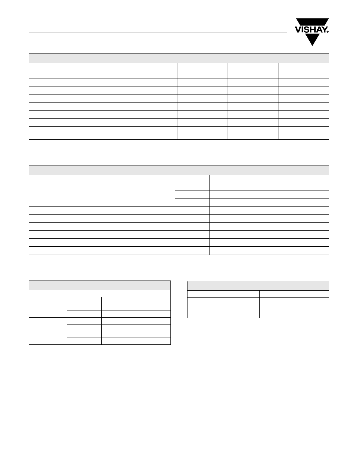
ABSOLUTE MAXIMUM RATINGS1), VLMS31..
PARAMETER TEST CONDITION SYMBOL VALUE UNIT
Reverse voltage
DC Forward current
Surge forward current
2)
≤ 85 °C I
T
amb
≤ 10 µs I
t
p
Power dissipation
Junction temperature
Operating temperature range
Storage temperature range
Thermal resistance junction/
ambient
Note:
1)
T
= 25 °C unless otherwise specified
amb
2)
Driving LED in reverse direction is suitable for short term application
mounted on PC board
(pad size > 16 mm
2
)
OPTICAL AND ELECTRICAL CHARACTERISTICS1), VLMS31.., RED
PARAMETER TEST CONDITION PART SYMBOL MIN TYP. MAX UNIT
Luminous intensity
2)
Dominant wavelength
Peak wavelength
Angle of half intensity
Forward voltage
Reverse voltage
Junction capacitance
Note:
1)
T
= 25 °C unless otherwise specified
amb
2)
in one Packing Unit I
Vmax/IVmin
≤ 2.0
IF = 10 mA
VLMS31J1K2
VLMS31J1L2
VLMS31K1L2
I
= 10 mA λ
F
= 10 mA λ
I
F
= 10 mA
I
F
I
= 20 mA V
F
= 10 μAV
I
R
= 0, f = 1 MHz C
V
R
T
R
V
FSM
P
T
amb
T
thJA
F
stg
R
6V
30 mA
0.1 A
V
j
80 mW
100 °C
- 40 to + 100 °C
- 40 to + 100 °C
400 K/W
I
V
I
V
I
V
d
p
4.5 11.2 mcd
4.5 18 mcd
7.1 18 mcd
624 630 638 nm
643 nm
ϕ ± 60 deg
F
R
j
5V
1.9 2.6 V
15 pF
LUMINOUS INTENSITY CLASSIFICATION
GROUP LIGHT INTENSITY [MCD]
STANDARD OPTIONAL MIN MAX
J 1 4.5 5.6
2 5.6 7.1
K 1 7.1 9.0
2 9.0 11.2
L 1 11.2 14
2 14 18
Note:
Luminous intensity is tested at a current pulse duration of 25 ms and
an accuracy of ± 11 %.
The above type numbers represent the order groups which include
only a few brightness groups. Only one group will be shipped on
each reel (there will be no mixing of two groups on each reel).
In order to ensure availability, single brightness groups will not be orderable.
In a similar manner for colors where wavelength groups are measured and binned, single wavelength groups will be shipped on any
one reel.
In order to ensure availability, single wavelength groups will not be
orderable.
www.vishay.com
2
CROSSING TABLE
VISHAY OSRAM
VLMS31J1K2 LST670-J1K2
VLMS31J1L2 LST670-J1L2
VLMS31K1L2 LST670-K1L2
Document Number 81327
Rev. 1.0, 17-Oct-06
Page 3
TYPICAL CHARACTERISTICS
p
T
= 25 °C unless otherwise specified
amb
VLMS31..
Vishay Semiconductors
60
50
40
30
20
- Forward Current (mA)
F
I
10
95 10905
0
T
- Ambient Temperature (°C)
amb
100806040200
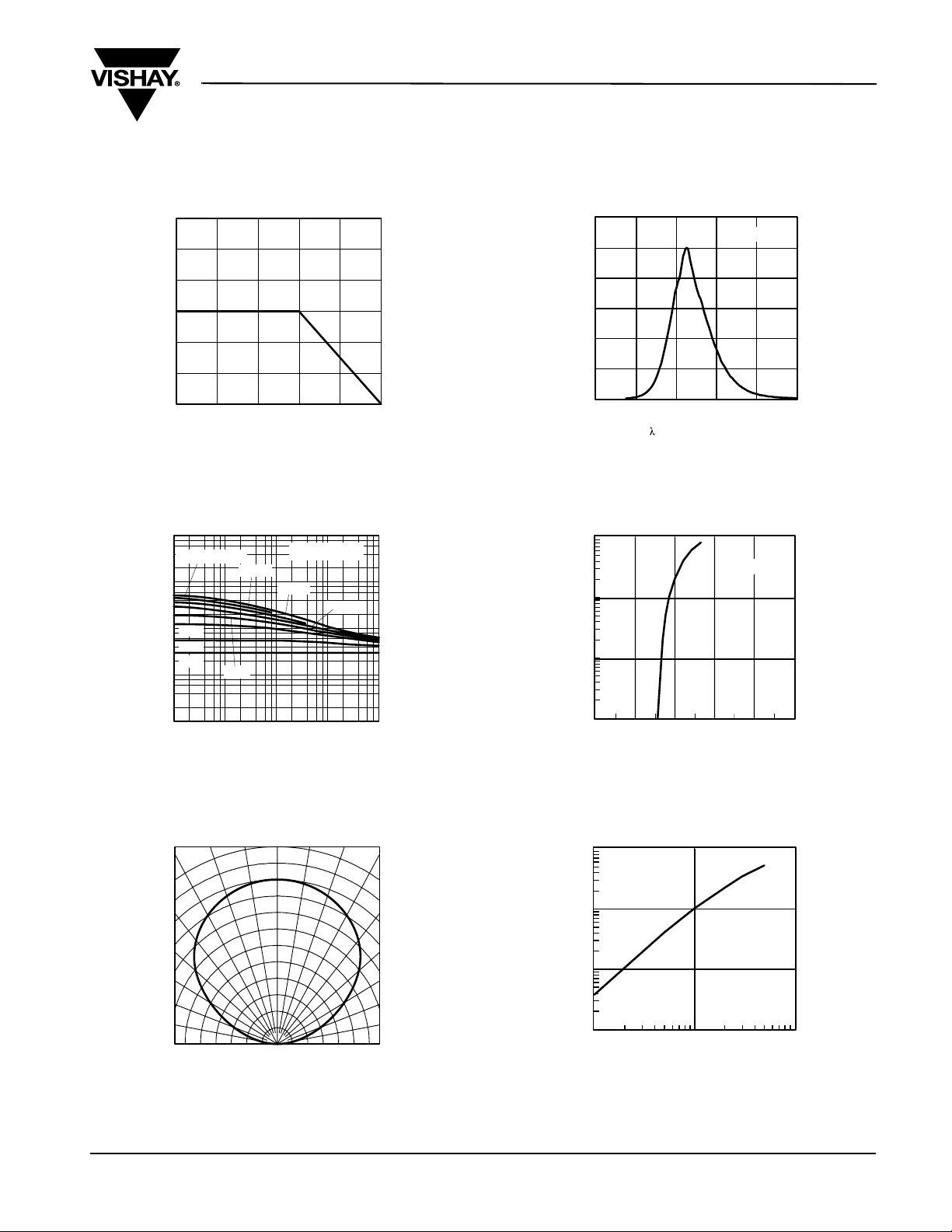
Figure 1. Forward Current vs. Ambient Temperature
10000
T
< 60 °C
tp/T = 0.005
1000
100
0.2
0.5
DC
10
F
I - Forward Current (mA)
1
0.01 0.1 1 10
95 9985
0.01
0.1
t
- Pulse Length (ms)
amb
0.02
0.05
100
Figure 2. Forward Current vs. Pulse Length
1.2
Super Red
1.0
0.8
0.6
0.4
0.2
Vrel
I –Relative Luminous Intensity
0.0
550 590 630 670 710 750
16639
– Wavelength (nm)
Figure 4. Relative Luminous Intensity vs. Wavelength
100
Super Red
10
1
F
I - Forward Current (mA)
0.1
012345
16634
V
-Forward Voltage (V)
F
Figure 5. Forward Current vs. Forward Voltage
0°
10° 20°
1.0
0.9
0.8
- Relative Luminous Intensity
0.7
V rel
I
95 10319
0.4 0.2 0 0.2 0.4
0.6
0.6
Figure 3. Rel. Luminous Intensity vs. Angular Displacement
Document Number 81327
Rev. 1.0, 17-Oct-06
30°
40°
50°
60°
70°
80°
10.00
Super Red
1.00
0.10
– Relative Luminous Intensity
Vrel
I
0.01
1.00 10.00 100.00
I
16638
– Forward Current (mA)
F
Figure 6. Relative Luminous Intensity vs. Forward Current
www.vishay.com
3
Page 4
VLMS31..
Vishay Semiconductors
2.0
Super Red
1.6
1.2
0.8
0.4
Vrel
I –Relative Luminous Intensity
0.0
0 20406080 100
– Ambient Temperature (°C)
T
16635
amb
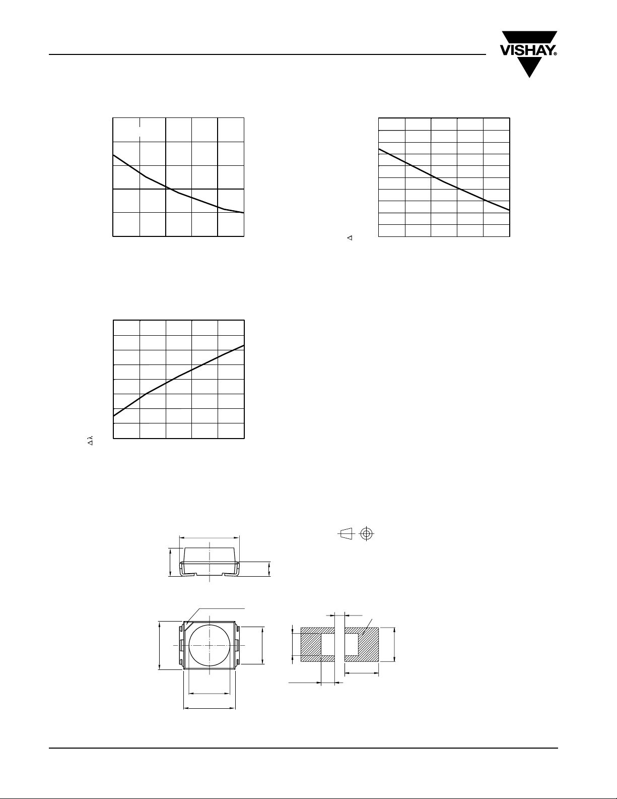
Figure 7. Rel. Luminous Intensity vs. Ambient Temperature
5
4
3
2
1
0
- 1
- 2
- Change of Dom. Wavelength (nm)
d
- 3
0 20406080 100
T
- Ambient Temperature (°C)
16637
amb
Figure 8. Change of Dominant Wavelength vs.
Ambient Temperature
200
150
100
50
0
- 50
- 100
- 150
- 200
- 250
F
V – Change of Forward Voltage (mV)
- 300
020406080 100
16636
T
- Ambient Temperature (°C)
amb
Figure 9. Change of Forward Voltage vs. Ambient Temperature
PACKAGE DIMENSIONS IN MM
3. 5 ± 0.2
0.10
1.75 ±
Pin identification
CA
+ 0.15
2.8
Ø 2.4
+ 0.15
3
Drawing-No. : 6.541-5025.01-4
Issue: 8; 22.11.05
95 11314-1
www.vishay.com
4
2.2
0.9
Mounting Pad Layout
2.6 (2.8)
1.6 (1.9)
technical drawings
according to DIN
specifications
1.2
4
area covered with
solder resist
4
Document Number 81327
Rev. 1.0, 17-Oct-06
Page 5
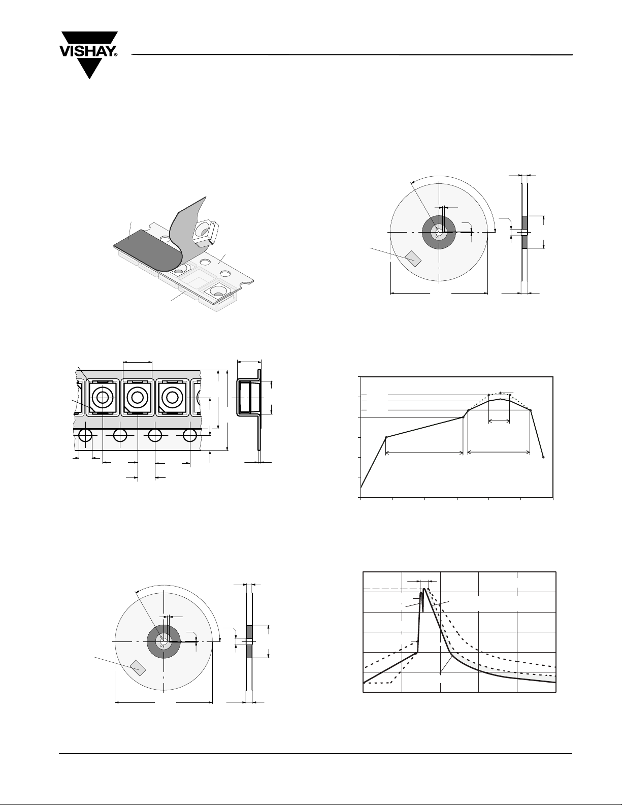
METHOD OF TAPING/POLARITY AND TAPE AND REEL
255
240 °C
217 °C
VLMS31..
Vishay Semiconductors
SMD LED (VLM3 - SERIES)
Vishay’s LEDs in SMD packages are available in an
antistatic 8 mm blister tape (in accordance with
DIN IEC 40 (CO) 564) for automatic component insertion. The blister tape is a plastic strip with impressed
component cavities, covered by a top tape.
Adhesive Tape
Blister Tape
Component Cavity
94 8670
TAPING OF VLM.3..
8.3
7.7
2.2
2.0
0.25
94 8668
4.0
3.6
3.5
4.1
3.9
3.1
2.05
1.95
4.1
3.9
1.85
1.65
Anode
Cathode
1.6
1.4
Figure 10. Tape dimensions in mm for PLCC-2
3.6
3.4
5.75
5.25
REEL PACKAGE DIMENSION IN MM FOR
SMD LEDS, TAPE OPTION GS08
(= 1500 PCS.)
10.0
13.00
12.75
14.4 max.
9.0
94 8665
63.5
60.5
Identification
Label:
Vishay
Type
Group
Tape Code
Production
Code
Quantity
120°
4.5
3.5
2.5
1.5
180
178
Figure 11. Reel dimensions - GS08
REEL PACKAGE DIMENSION IN MM FOR
SMD LEDS, TAPE OPTION GS18
(= 8000 PCS.) PREFERED
10.4
13.00
12.75
14.4 max.
8.4
62.5
60.0
18857
Identification
Label:
Vishay
Type
Group
Tape Code
Production
Code
Quantity
321
329
120°
4.5
3.5
2.5
1.5
Figure 12. Reel dimensions - GS18
SOLDERING PROFILE
IR Reflow Soldering Profile for lead (Pb)-free soldering
Preconditioning acc. to JEDEC Level 2a
300
255 °C
250
200
150
Temperature (°C)
100
50
0
0 50 100 150 200 250 300
19885
max. 120 s
max. Ramp Up 3 °C/s
Time (s)
max. 100 s
max. Ramp Down 6 °C/s
Figure 13. Vishay Lead (Pb)-free Reflow Soldering Profile
(acc. to J-STD-020C)
300
250
200
150
100
Temperature (°C)
50
0
TTW Soldering
235 °C...260 °C
first wave
ca. 200 K/s
100 °C...130 °C
0
(acc. to CECC00802)
5 s
2 K/s
forced cooling
50
100
second
wave
ca. 2 K/s
Time (s)
dotted line: process limits
150
Figure 14. Double wave soldering of opto devices (all packages)
max. 260 °C
245 °C
max. 30 s
max. 2 cycles allowed
948626-1
Lead Temperature
full line: typical
ca. 5 K/s
200
250
Document Number 81327
Rev. 1.0, 17-Oct-06
www.vishay.com
5
Page 6
VLMS31..
Vishay Semiconductors
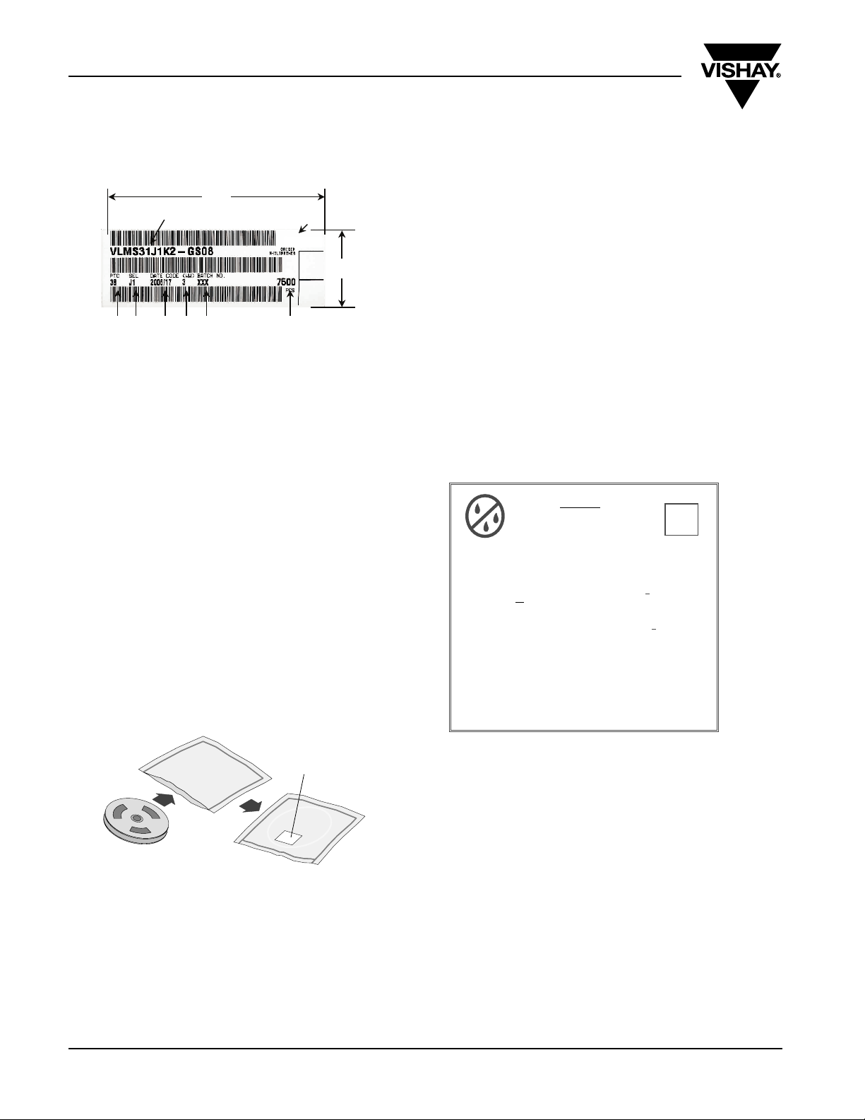
BARCODE-PRODUCT-LABEL
106
A
BC D E F G
H
VISHAY
37
20127
A) Type of component
B) Manufacturing plant
C) SEL - Selection Code (Bin):
e.g.: J1 = Code for Luminous Intensity Group
D) Date Code year/week
E) Day Code (e.g. 3: Wednesday)
F) Batch No.
G) Total quantity
H) Company Code
DRY PACKING
The reel is packed in an anti-humidity bag to protect
the devices from absorbing moisture during transportation and storage.
Aluminium bag
RECOMMENDED METHOD OF STORAGE
Dry box storage is recommended as soon as the aluminium bag has been opened to prevent moisture
absorption. The following conditions should be
observed, if dry boxes are not available:
• Storage temperature 10 °C to 30 °C
• Storage humidity ≤ 60 % RH max.
After more than 672 hours under these conditions
moisture content will be too high for reflow soldering.
In case of moisture absorption, the devices will recover
to the former condition by drying under the following
condition:
192 hours at 40 °C + 5 °C/ - 0 °C and < 5 % RH
(dry air/nitrogen) or
96 hours at 60 °C + 5 °C and < 5 % RH for all device
containers or
24 hours at 100 °C + 5 °C not suitable for reel or tubes.
An EIA JEDEC Standard JESD22-A112 Level 2a label
is included on all dry bags.
CAUTION
1. Shelf life in sealed bag 12 months at <40°C and < 90% relative humidity (RH)
2. After this bag is opened devices that will be subjected to infrared reflow,
vapor-phase reflow, or equivalent processing (peak package body temp.
260°C) must be:
a) Mounted within
b) Stored at <1
3. Devices require baking before mounting if:
a) Humidity Indicator Card is >10% when read at 23°C +
b) 2a or 2b is not met.
4. If baking is required, devices may be baked for:
192 hours
96 hours
24 hours
Bag Seal Date: ______________________________
(If blank, see bar code label)
This bag contains
MOISTURE –SENSITIVE DEVICES
672 hours
0% RH.
at 40°C + 5°C/-0°C and <5%RH (dry air/nitrogen)
at 60±5
at 100±5°C Not suitable for
Note: LEVEL defined by EIA JEDEC Standard JESD22-A113
at factory condition of <
o
Cand <5%RH For
all
device containers or
L E V E L
2a
30°C/60%RH or
5°C or
reels or tubes
or
19786
Example of JESD22-A112 Level 2a label
Label
Reel
15973
FINAL PACKING
The sealed reel is packed into a cardboard box. A secondary cardboard box is used for shipping purposes.
www.vishay.com
6
ESD PRECAUTION
Proper storage and handling procedures should be followed to prevent ESD damage to the devices especially when they are removed from the Antistatic
Shielding Bag. Electro-Static Sensitive Devices warning labels are on the packaging.
VISHAY SEMICONDUCTORS STANDARD
BAR-CODE LABELS
The Vishay Semiconductors standard bar-code labels
are printed at final packing areas. The labels are on
each packing unit and contain Vishay Semiconductors
specific data.
Document Number 81327
Rev. 1.0, 17-Oct-06
Page 7

VLMS31..
Vishay Semiconductors
OZONE DEPLETING SUBSTANCES POLICY STATEMENT
It is the policy of Vishay Semiconductor GmbH to
1. Meet all present and future national and international statutory requirements.
2. Regularly and continuously improve the performance of our products, processes, distribution and operating
systems with respect to their impact on the health and safety of our employees and the public, as well as their
impact on the environment.
It is particular concern to control or eliminate releases of those substances into the atmosphere which are known as
ozone depleting substances (ODSs).
The Montreal Protocol (1987) and its London Amendments (1990) intend to severely restrict the use of ODSs and
forbid their use within the next ten years. Various national and international initiatives are pressing for an earlier ban
on these substances.
Vishay Semiconductor GmbH has been able to use its policy of continuous improvements to eliminate the use of
ODSs listed in the following documents.
1. Annex A, B and list of transitional substances of the Montreal Protocol and the London Amendments respectively
2. Class I and II ozone depleting substances in the Clean Air Act Amendments of 1990 by the Environmental
Protection Agency (EPA) in the USA
3. Council Decision 88/540/EEC and 91/690/EEC Annex A, B and C (transitional substances) respectively.
Vishay Semiconductor GmbH can certify that our semiconductors are not manufactured with ozone depleting
substances and do not contain such substances.
We reserve the right to make changes to improve technical design
and may do so without further notice.
Parameters can vary in different applications. All operating parameters must be validated for each customer
application by the customer. Should the buyer use Vishay Semiconductors products for any unintended or
unauthorized application, the buyer shall indemnify Vishay Semiconductors against all claims, costs,
damages, and expenses, arising out of, directly or indirectly, any claim of personal damage, injury or death
associated with such unintended or unauthorized use.
Vishay Semiconductor GmbH, P.O.B. 3535, D-74025 Heilbronn, Germany
Document Number 81327
Rev. 1.0, 17-Oct-06
www.vishay.com
7
Page 8

Legal Disclaimer Notice
Vishay
Notice
Specifications of the products displayed herein are subject to change without notice. Vishay Intertechnology, Inc.,
or anyone on its behalf, assumes no responsibility or liability for any errors or inaccuracies.
Information contained herein is intended to provide a product description only. No license, express or implied, by
estoppel or otherwise, to any intellectual property rights is granted by this document. Except as provided in Vishay's
terms and conditions of sale for such products, Vishay assumes no liability whatsoever, and disclaims any express
or implied warranty, relating to sale and/or use of Vishay products including liability or warranties relating to fitness
for a particular purpose, merchantability, or infringement of any patent, copyright, or other intellectual property right.
The products shown herein are not designed for use in medical, life-saving, or life-sustaining applications.
Customers using or selling these products for use in such applications do so at their own risk and agree to fully
indemnify Vishay for any damages resulting from such improper use or sale.
Document Number: 91000 www.vishay.com
Revision: 08-Apr-05 1
 Loading...