

Page 1
Corporate: www.cd techno.com
Corporate: www.cd techno.com
Product: www.cd poweronline.com
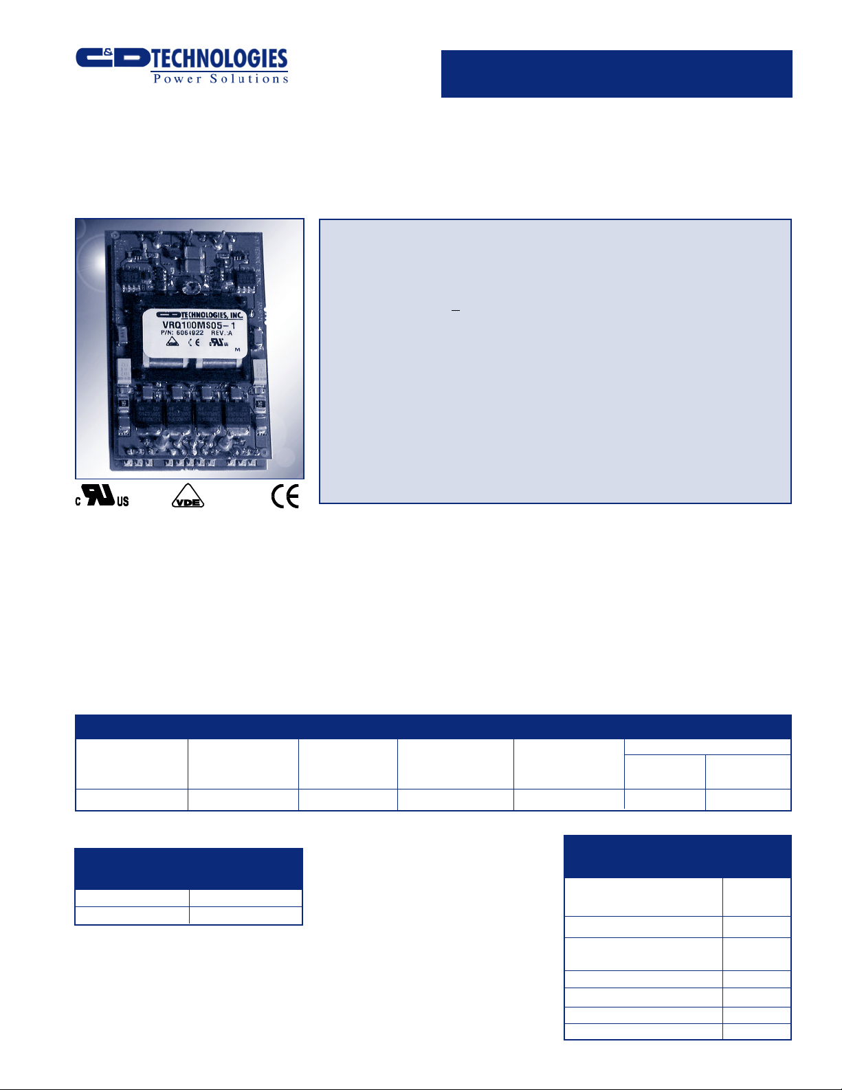
VKQ100MS05
100 Watt, 5.0Vout, Quarter Brick DC/DC Converter
The VKQ100MS05 DC/DC converter
presents an economical and practical
solution for distributed power system
architectures which require high power
density and efficiency while maintaining
system modularity and upgradeability.
With the ability to operate over a wide
input voltage range of 36 to 75 Vdc, this
module is ideal for telecommunications
and battery backup applications where
FEATURES
36 - 75V Input Range
Small Size: 1.5" x 2.3" x .50"
High Efficiency: >86%
Fixed Frequency Operation
480kHz
Primary Remote On/Off
Adjustable Output Voltage
Brick Wall Current Limiting
On Board Input Differential
Filter
No Minimum Load Requirement
Remote Sense
input flexibility must be combined with
output voltage regulation. In addition, the
output is fully isolated from the input,
allowing for a variety of polarity and
grounding configurations.
Innovative circuit design using surface
mount components results in a compact,
efficient and reliable solution to DC/DC
conversion needs. Internal power
dissipation is minimized by the
No Heatsink Required
No External Components
Required
Safety per UL/CUL 60950,
EN 60950, Operational
Insulation Meets TNV-SELV
Isolation Requirements
APPLICATIONS
Distributed Power Architectures
Telecommunications
Battery Powered Systems
Workstations
VKQ100MS05’s high efficiency and is
aided by a metal baseplate to which all
heat dissipative elements are coupled.
The control circuitry of the
VKQ100MS05 has been designed to
provide overvoltage protection as well as
current limiting for continuous shortcircuit protection.
PRODUCT SELECTION CHART
NOMINAL INPUT RATED OUTPUT RATED OUTPUT INPUT CURRENT EFFICIENCY
VOLTAGE VOLTAGE CURRENT NOM MIN TYP
MODEL (VDC) (VDC) (A) (A) (%) (%)
VKQ100MS05 48 5.0 20 2.40 86 86.5
ORDERING
INFORMATION
MODEL NO. PART NO.
VKQ100MS05 6064922
VKQ100MS05 -1 REV A 4/2003
ABSOLUTE MAX.
RA TINGS
Output Short-Circuit
Duration Continuous
Internal Power Dissipation 16.3 Watts
Lead Temperature
(soldering, 10 seconds max) +300°C
Continuous Input Voltage 75 VDC
Storage Temperature +125°C
Input to Output Isolation 1500 VDC
Input Voltage (non-operating) 100 VDC
Page 2
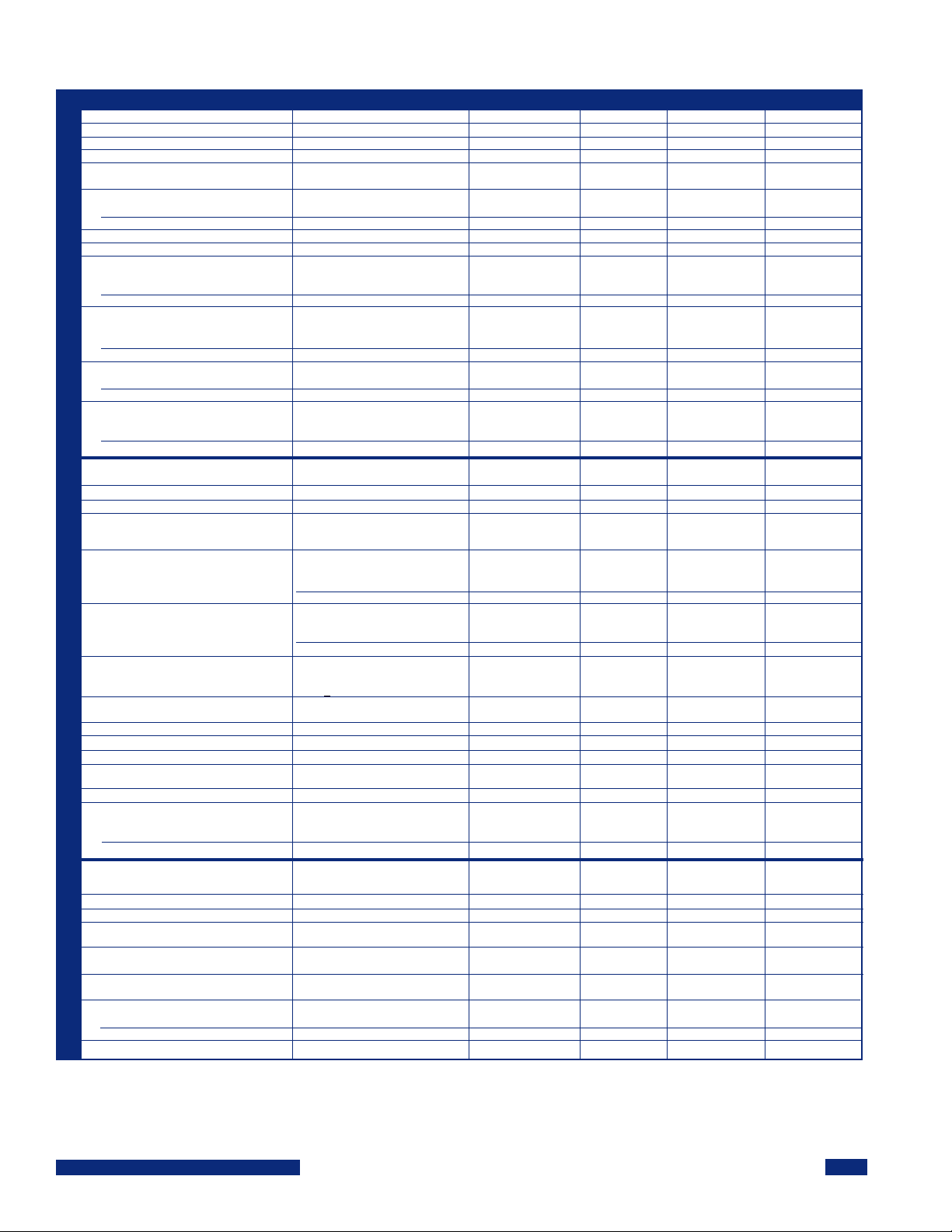
SPECIFICATIONS
Unless otherwise specified, all specifications are at TA = +25°C.
PARAMETER CONDITIONS MIN NOM MAX UNITS
Voltage Range (Vin) 36 48 75 Vdc
Reflected Ripple Current
Input Ripple Rejection (100 Hz – 1KHz) Vin = 48 Vdc; Io = 20 A. -30 dB
No Load Input Current Vin = 48 Vdc; Io = 0 A. 90 100 mA
Quiescent Input Current
Primary On/Off Disabled Vin = 48 Vdc; Io = 20 A. 4 mA
Power Dissipation Vin = 48 Vdc.
No Load 4.85 5.30 W
Standby, Primary On/Off Disabled 0.20 W
Maximum Input Current Vin = 36 Vdc; Io = 20 A. 3.40 A
Inrush Charge Vin = 75 Vdc. 0.165 mC
Input Under Voltage Protection Tamb = -40°C to +60°C;
Shut down 31.50 32.50 Vdc
Turn On 32.50 33.70 Vdc
Input Over Voltage Protection Tamb = -40°C to +60°C;
INPUTOUTPUT
Shut down 76.50 79.00 Vdc
Turn On 76.00 78.00 Vdc
Input Under Voltage Protection Tamb = +25°C; Io = 0A to 20A
Shutdown 32.00 32.25 Vdc
Turn On 33.00 33.50 Vdc
Input Over Voltage Protection Tamb = -40°C to +60°C;
Shut down 77.70 79.00 Vdc
Turn On 76.20 77.60 Vdc
OUTPUT
Nominal Voltage (Vnom) 5.00 Vdc
Output Current (Io)
Rated Power
Set Point Accuracy Vin = 48 Vdc; Io = 10 A;
Line Regulation Vin = 36 Vdc to 75 Vdc;
Load Regulation Vin = 36 Vdc to 75 Vdc;
Ripple & Noise
Temperature Drift Tamb = -40°C to +60°C;
Current Limit Inception Vin = 48 Vdc. 21.50 24.00 A
Short Circuit Current Vin = 48 Vdc. 21.00 24.00 A
Output Voltage Adjust Range Vin = 48 Vdc; Io = 0-20 A -10 +10 %Vnom
Turn – On Time Vin = 48 Vdc; Io = 0-20 A
Over Voltage Protection Set Point Vin = 48 Vdc; Io = 20 A. 6.60 7.10 Vdc
Transient Response 50% to 100% Load Step to
Peak Deviation Co = 1000µF; Vin = 48Vdc 210 mV
Settling Time 70 µS
2
3
1
2
Vin = 48 Vdc; Io = 20 A. 4 A pk-pk
Io = 0 A to 20 A
Io = 0 A to 20 A
Io = 0 A to 20 A
Vin = 36 Vdc to 75 Vdc. 0 20 A
Vin = 36 Vdc to 75 Vdc. 0 100 W
Tamb = -40°C to +60°C. 1 % of Vnom
T amb = +25°C 0.50 % of Vnom
Tamb = -40°C to +60°C;
Io = 20 A. 0.02 0.20 % of Vnom
T amb = +25°C 0.01 0.05 % of Vnom
Io = 0 A to 20 A.
Tamb = -40°C to +60°C; 0.15 0.30 % of Vnom
Tamb = +25°C; Vin = 48Vdc 0.01 0.05 % of Vnom
Vin = 36-75 Vdc; Io = 0-20 A;
TA = -40°C to +60°C
f
< 20 MHz Bandwidth. 120 mV pk-pk
Vin = 48 Vdc; Io = 20 A. 0.005 0.01 % / °C
Output to within 1% of Vnom 1.00 1.40 ms
di/dt = 75A/µS;
GENERAL
Efficiency
Switching Frequency Vin = 36 Vdc-75 Vdc; Io = 0-20 A 460 480 500 KHz
Remote Sense Compensation Vin = 48 Vdc 0.500 Vdc
Remote On / Off Control Inputs Vin = 36 Vdc-48 Vdc; Io = 0-20 A
Primary
Sink Current – Logic Low 0.60 1.60 mA
Vlow 0.70 0.75 Vdc
Vhigh N/A N/A N/A Open Collector
GENERAL
Calculated MTTF Vin = 48 Vdc; Io = 20 A
Per Telcordia TR-NWT-000332 TBD Hours
Per MIL=HDBK217E TBD Hours
Operating Ambient Temperature -40 +70 °C
4
Product: www.cdpoweronline.com
Vin = 48 Vdc; Io = 20 A. 86 %
Tamb = -40°C to +60°C
VKQ100MS05 REV A 4/2003
2
Page 3
SPECIFICATIONS Unless otherwise specified, all specifications are at T
= +25°C.
A
PARAMETER CONDITIONS MIN NOM MAX UNITS
ISOLATION
Input to Output 1500 Vdc
Input to Base Plate 1500 Vdc
Output to Base Plate 500 Vdc
Resistance Input to Output 10 MΩ
Capacitance Input to Output 2000 pF
ISOLA TION
Leakage Current V(input – output) = 240 Vac, 60 Hz 180 µA, rms
Notes:
1. A future Application Note will detail the technique used to measure the reflected ripple current.
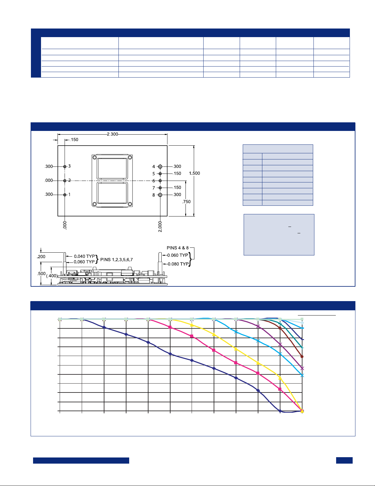
2. Refer to Power Derating Curve below for details on Output Current Derating with Ambient Temperature. A future Application Note will detail air flow
characterization.
3. Refer to performance curves section (pages 4 and 5) for variation in output ripple and noise with Ambient Temperature, Input Voltage and Output Current. The
unit requires a ceramic capacitor of 0.022µFacross measurement terminals. A future Application Note will detail measurement set up for output ripple and noise.
4. Refer to performance curves section for variation in efficiency against Input Voltage, Ambient Temperature, Output Load and Frequency.
MECHANICAL
VKQ100MS05 (6064922)
PIN ASSIGNMENT
No. Function
1 +Vin
2 On/Off
3 -Vin
4 -Vout
5 -Sense
6 Trim
7 +Sense
8 +Vout
PIN SIDE UP
NOTES:
General Tolerance: +.020
Pin Location Tolerance: +.010
Unit Weight: 34g / 1.2oz.
PIN MATERIAL: COPPER
PIN FINISH: TIN-LEAD
POWER DERA TING CURVE (Vin = 36Vdc - 75Vdc)
20.0
18.0
16.0
14.0
12.0
10.0
8.0
6.0
Output Current (A)
4.0
2.0
0.0
-40-30-20-10 0 10203040506070
Temperature (Deg 0C)
30/0.3
80/0.7
Air Speed LFM/CFM
900/7.8
800/6.9
700/6.1
600/5.2
500/4.3
400/3.5
300/2.6
200/1.7
100/0.9
Product: www.cdpoweronline.com
VKQ100MS05 REV A 4/2003
3
Page 4
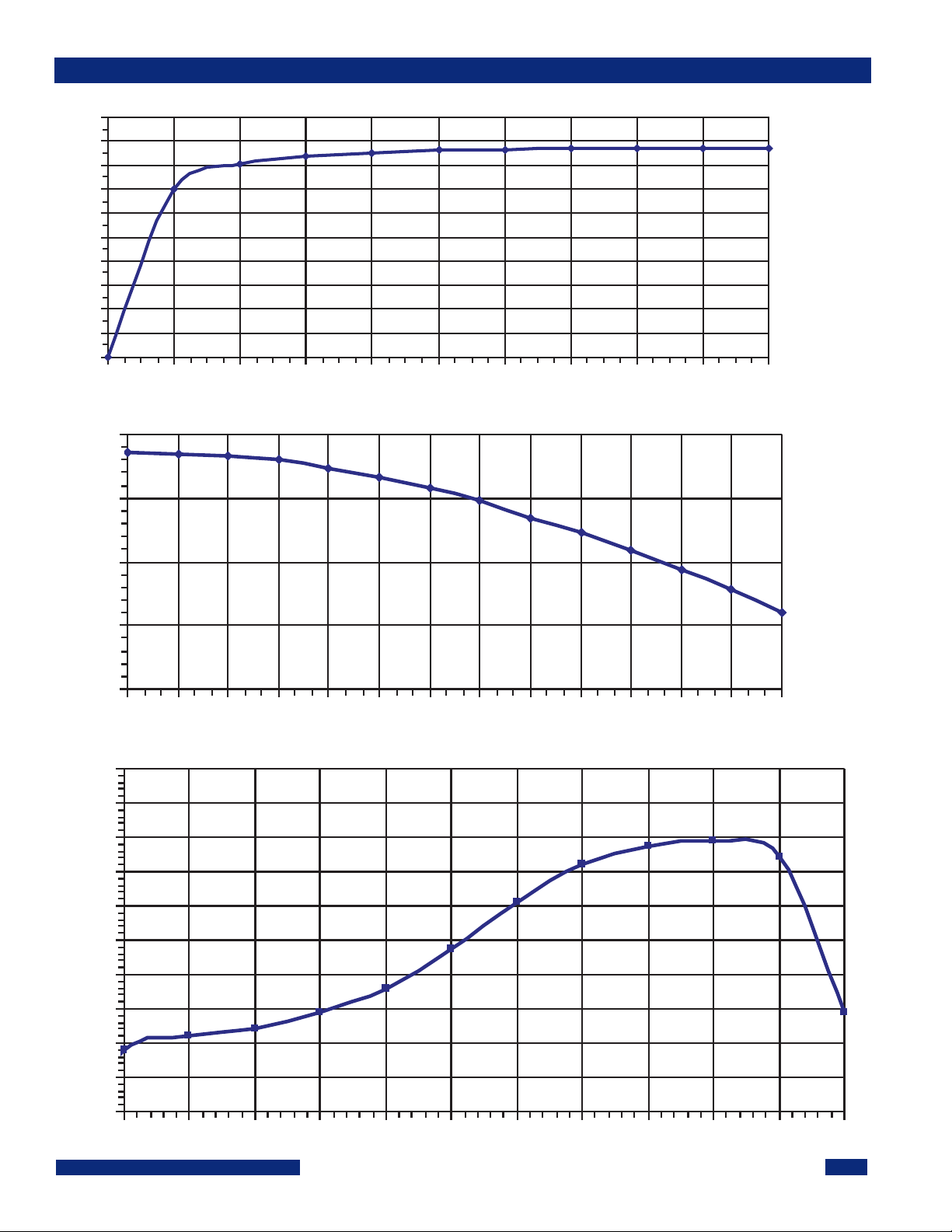
TYPICAL PERFORMANCE CURVES
100
EFFICIENCY (%) vs. OUTPUT CURRENT (A) @ TA +250C; Vin = 48Vdc
90
80
70
60
50
40
Efficiency (%)
30
20
10
0
0 2 4 6 8 101214161820
Output Current (A)
87.00
86.50
EFFICIENCY (%) vs. INPUT VOL T AGE @ TA +250C; Io = 20A
86.00
Efficiency (%)
85.50
85.00
36 39 42 45 48 51 54 57 60 63 66 69 72 75
87.0
86.9
86.8
86.7
86.6
86.5
86.4
Efficiency (%)
86.3
Input V oltage (Vdc)
EFFICIENCY (%) vs. AMBIENT TEMP. (0C) @ Vin = 48Vdc; Io = 20A
86.2
86.1
86.0
-40-30-20-10 010 2030 4050 6070
T emperature (0C)
Product: www.cdpoweronline.com
VKQ100MS05 REV A 4/2003
4
Page 5
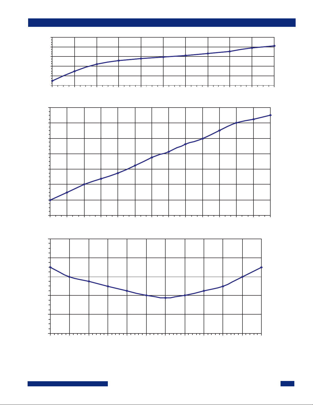
OUTPUT RIPPLE & NOISE (mV pk-pk) vs. OUTPUT LOAD (A) @ 20MHz; TA +250C; Vin = 48Vdc
100
80
60
40
O/P Ripple &
20
Noise (mV pk-pk)
0
0 2 4 6 8 10 12 14 16 18 20
OUTPUT RIPPLE & NOISE (mV pk-pk) vs. INPUT VOL TAGE (Vdc) @ 20MHz; TA +250C; Io = 20A
90
88
86
84
82
TYPICAL PERFORMANCE CURVES
Output Load (A)
80
O/P Ripple & Noise (mV pk-pk)
78
76
36 39 42 45 48 51 54 57 60 63 66 69 72 75
OUTPUT RIPPLE & NOISE (mV pk-pk) vs. AMBIENT TEMP. (0C) @ 20MHz; Vin = 48Vdc; Io = 20A
100
Input V oltage (Vdc)
96
92
88
84
O/P Ripple & Noise (mV pk-pk)
80
-40 -30 -20 -10 0 10 20 30 40 50 60 70
Ambient T emperature (0C)
Power Electronics Division, Americas
3400 E Britannia Drive, Tucson, Arizona 85706
Any data, prices, descriptions or specifications presented herein are subject to revision by C&D T echnologies, Inc. without notice. While such information is believed to be accurate as indicated herein, C&D
Technologies, Inc. makes no warranty and hereby disclaims all warranties, express or implied, with regard to the accuracy or completeness of such information. Further , because the product(s) featured herein may
be used under conditions beyond its control, C&D T echnologies, Inc. hereby disclaims all warranties, either express or implied, concerning the fitness or suitability of such product(s) for any particular use or in any
specific application or arising from any course of dealing or usage of trade. The user is solely responsible for determining the suitability of the product(s) featured herein for user’s intended purpose and in user’s
specific application. C&D Technologies, Inc. does not warrant or recommend that any of its product s be used in any life support or aviation or aerospace applications.
Product: www.cdpoweronline.com
Tel: 800.547.2537 Fax: 520.295.4197
VKQ100MS05 REV A 4/2003
C&D Technologies, EMEA/Asia/Pacific
Milton Keynes MK14 5BU UK
T el: +44 (0)1908 615232 Fax: +44 (0)1908 617545
5
 Loading...