

Page 1
VIPer100B
TYPE V
DSS
I
R
n
DS(on)
VIPe r100B/BS P 400V 6 A 1.1 Ω
FEATURE
■ ADJUSTABLESWITCHINGFREQUENCYUP
TO200KHZ
■ CURRENT MODE CONTROL
■ SOFTSTART AND SHUT DOWN CONTROL
■ AUTOMATIC BURST MODE OPERATION IN
STAND-BY CONDITIONABLE TO MEET
”BLUE ANGEL” NORM (<1W TOTAL POWER
CONSUMPTION)
■ INTERNALLY TRIMMEDZENER
REFERENCE
■ UNDERVOLTAGE LOCK-OUT WITH
HYSTERESIS
■ INTEGRATED START-UPSUPPLY
■ AVALANCHERUGGED
■ OVERTEMPERATUREPROTECTION
■ LOW STAND-BYCURRENT
■ ADJUSTABLECURRENTLIMITATION
VIPer100BSP
SMPS PRIMARY I.C.
PRELIMINARY DATA
10
PENTAWATTHV PENTAWATT HV
PowerSO-10
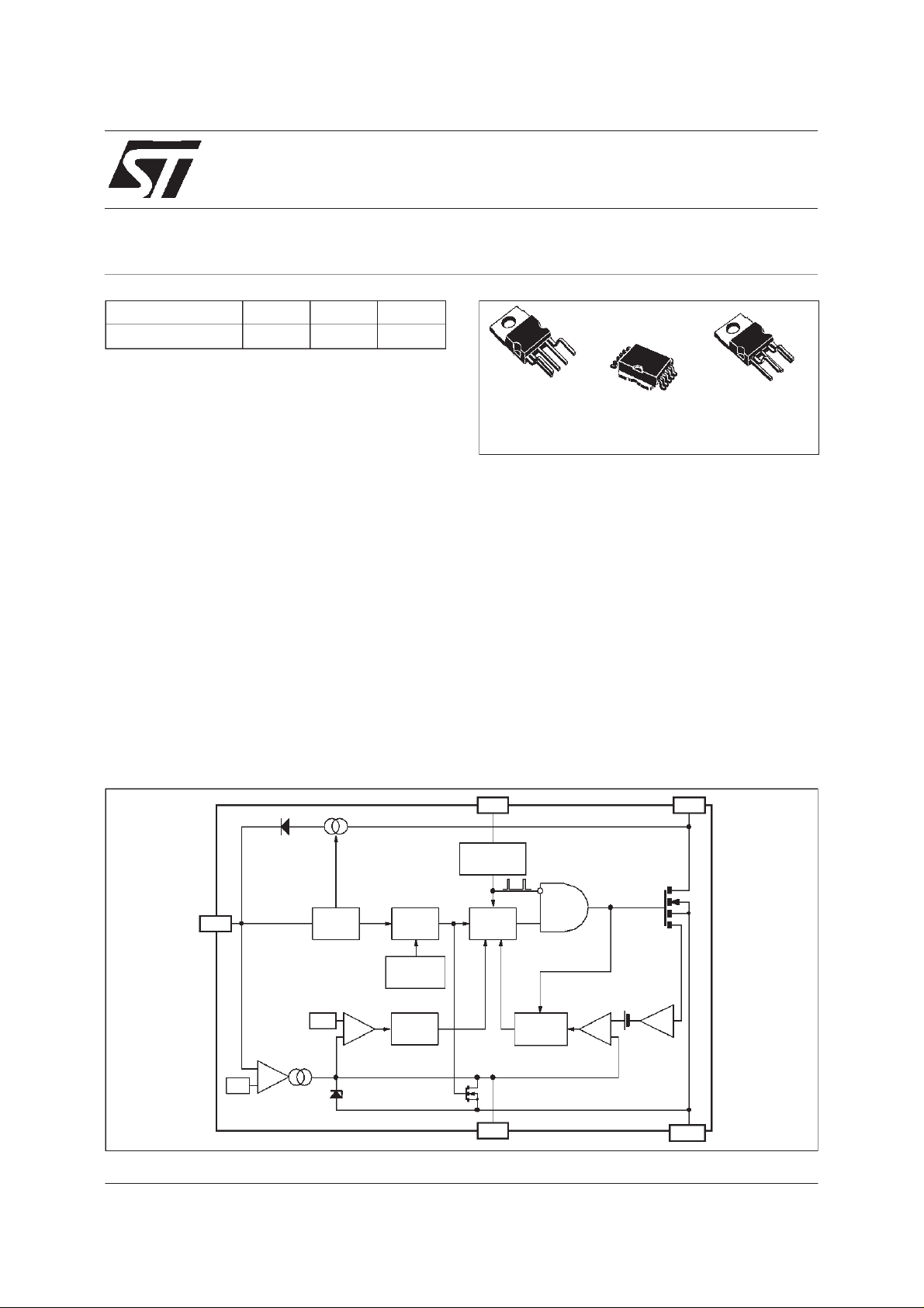
DESCRIPTION
VIPer100B/100BSP, made using VIPower M0
Technology, combines on the samesiliconchip a
state-of-the-art PWM circuit together with an
optimized high voltageavalanche rugged Vertical
Power MOSFET (400 V / 6 A). Typical
applications cover off line power supplies with
a secondary power capability of 100 W in a US
mains lines configuration. It is compatible from
both primaryor secondaryregulationloop despite
using around 50% less components when
compared with a discrete solution. Burst mode
operation is an additional feature of this device,
offering the possibility to operate in stand-by
mode without extra components.
1
(022Y)
BLOCK DIAGRAM
DD
V
January 2000
13 V
ERROR
AMPLIFIER
_
+
UVLO
LOGIC
0.5 V +
ON/OFF
_
4.5 V
SECURITY
LATCH
FF
Q
R/S
S
OVERTEMP.
DETECTOR
s
µ
1.7
DELAY
OSC
OSCILLATOR
PWM
LATCH
S
R1
FF
R2 R3
COMP
Q
250 ns
BLANKING
0.5V
+
_
_
+
CURRENT
AMPLIFIER
0.5V/A
DRAIN
SOURCE
1
3
2
0
0
C
F
1/20
Page 2
VIPER100B/BSP
ABSOLUTEMAXIMUM RATING
Symbol Para met e r Val u e Uni t
V
I
V
V
OSC
V
COMP
I
COMP
V
I
D(AR)
P
T
T
THERMALDATA
R
thj-case
R
thj-a mb.
(*) When mounted using the minimum recommended pad size on FR-4 board.
Continuous Dr ain -S ou r ce Voltage (Tj = 25 to 125oC) -0.3 to 400 V
DS
Maximum Current Internally Limited A
D
Supply Volt age 0 to 15 V
DD
Volt a ge Range Input 0 to V
DD
Volt a ge Range Input 0 t o 5 V
Maximum Continuous Current ±2mA
Electrostatic d ischarge (R = 1.5 KΩ C = 100p F )
esd
Avalanche Drain-Source Current , Repetiti ve or No t-R epetitiv e
=100oC, Pulse Width Limite d by TJmax, δ <1%)
(T
C
Power Dissi pation at T c = 25oC82W
tot
Junction Oper ating Tempera tu r e Int er na lly Lim it e d
j
St orage Temperat u r e -65 to 15 0
stg
4000 V
3A
PENTAWATT-HV PowerSO-10(*)
Ther mal Resistanc e Junction-c a se Max 1.4 1.4
Ther mal Resistanc e Am bi ent-case Max 60 50
o
o
o
C/W
o
C/W
V
C
C
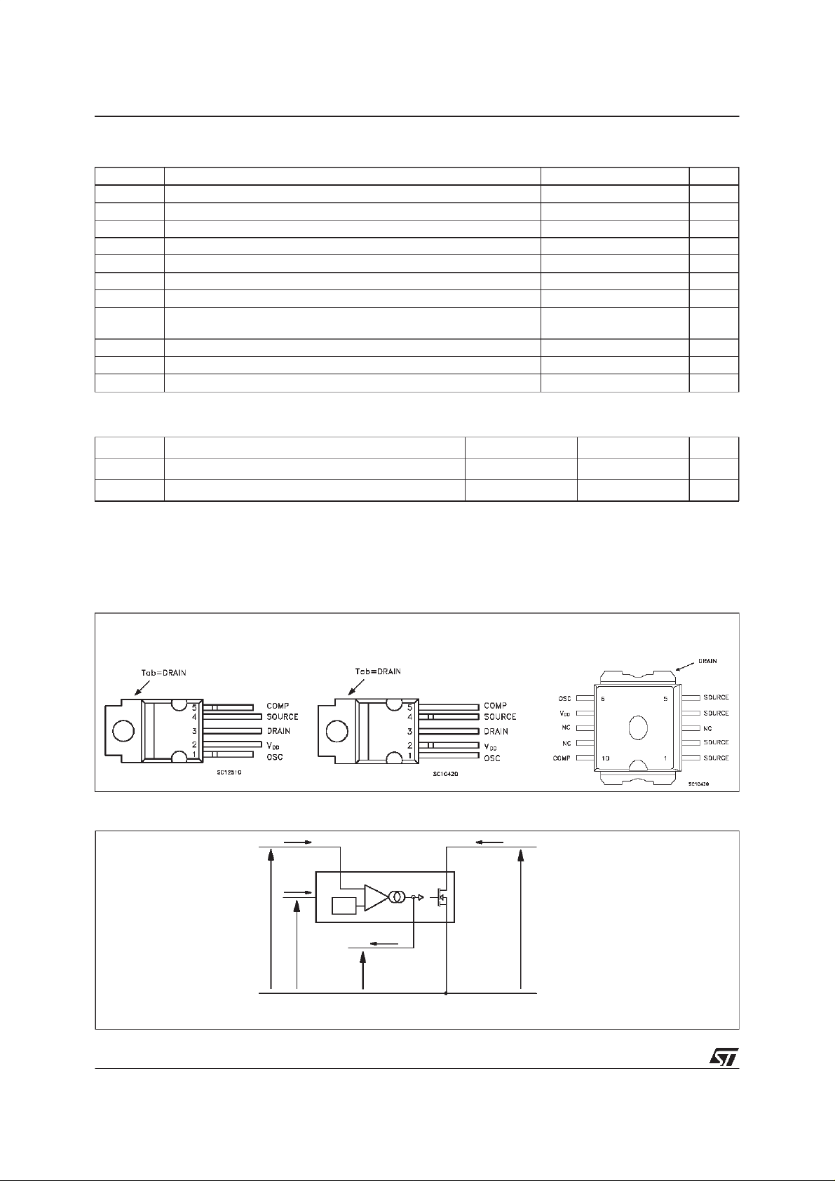
CONNECTION DIAGRAMS(Top View)
PENTAWATTHV PENTAWATTHV (022Y) PowerSO-10
CURRENT AND VOLTAGE CONVENTIONS
IDD ID
OSC
I
OSC
DD
V
13V
OSC
V
+
ICOMP
VCOMP
DRAINVDD
COMP SOURCE
VDS
2/20
FC00020
Page 3

ORDERING NUMBERS
PENTAW AT T HV PENT AWAT T HV (0 22Y) Pow erSO-10
VIP er 1 00B VIPe r 10 0B (0 22Y) VIPe r 100 B SP
VIPER100B/BSP
PINSFUNCTIONAL DESCRIPTION
DRAINPIN:
Integrated power MOSFET drain pin. It provides
internal bias current during start-up via an
integrated high voltage current source which is
switched off during normal operation.The device
is able to handle an unclamped current during its
normal operation, assuring self protection against
voltage surges, PCB stray inductance, and
allowing a snubberless operation for low output
power.
SOURCEPIN:
Power MOSFET source pin. Primary side circuit
commongroundconnection.
VDD PIN :
This pin providestwo functions:
- It corresponds to the low voltage supply of the
controlpart of the circuit. If V
the start-up current source is activatedand the
output power MOSFET is switched off untilthe
voltage reaches 11V. During this phase,
V
DD
the internal current consumption is reduced,
the V
pin is sourcing a currentof about 2mA
DD
and the COMP pin is shorted to ground. After
that, the current source is shut down, and the
devicetries to startup by switchingagain.
goes below 8V,
DD
- Thispin isalso connectedto the error amplifier,
in order to allow primary as well as secondary
regulation configurations. In case of primary
regulation, an internal 13V trimmed reference
voltage is used to maintain V
secondary regulation, a voltage between 8.5V
and 12.5V will be put on V
transformerdesign, in orderto stuckthe output
of the transconductance amplifier to the high
state. The COMP pin behaves as a constant
at 13V. For
DD
DD
pin by
current source, and can easily be connectedto
the output of an optocoupler. Note that any
overvoltage due toregulation loop failure is still
detected by the error amplifier through the V
DD
voltage, which cannot overpass 13V. The
output voltage will be somewhat higher than
the nominalone, but still under control.
COMP PIN :
This pin provides two functions :
- It is the output of the error transconductance
amplifier, and allows for the connection of a
compensation network to provide the desired
transfer function of the regulation loop. Its
bandwidth can be easily adjusted to the
needed value withusual componentsvalue. As
stated above, secondary regulation
configurations are also implemented through
the COMP pin.
- When the COMP voltage is going below 0.5V,
the shut-downof the circuit occurs, with a zero
duty cycle for the power MOSFET.This feature
can be used to switch off the converter, and is
automatically activated by the regulation loop
(whatever is the configuration) to provide a
burst mode operation in case of negligible
output power or openload condition.
OSC PIN :
An R
to define the switching frequency. Note that
despite the connection of R
significant frequency change occurs for V
varying from 8V to 15V. It provides also a
synchronisationcapability, when connectedto an
external frequencysource.
network must be connected on that pin
T-CT
to VDD,no
T
DD
3/20
Page 4
VIPER100B/BSP
AVALANCHE CHARACTERISTICS
Symbol Para met e r Max Valu e Uni t
I
D(ar)
E
Avalanche Curre nt , Rep et itive or Not - Re petitive
(pulse width limited by T
Single Pulse Avalanche Energy
(ar)
(starting T
=25oC, ID=I
j
max, δ <1%)
j
) (see fig.12)
D(ar)
ELECTRICAL CHARACTERISTICS (TJ=25oC, VDD=13 V, unless otherwise specified)
POWERSECTION
Symbol Pa ram et e r Test Con d i ti ons Mi n . Typ . Ma x. Unit
BV
I
DSS
R
DS(on)
C
OSS
(1) On Inductive Load, Clamped.
Drain-Source Voltage ID=1mA V
DSS
Off -St ate Drain Current V
St at i c Drain Source o n
Resistance
t
Fall Time ID=0.2AVin= 3 00 V ( 1)
f
=0V TJ= 125oC
COMP
=400V 1 mA
V
DS
ID=4A
=4A TJ=100oC
I
D
= 0 V 400 V
COMP
(see fig.3)
Rise Tim e ID=4A Vin= 3 00 V ( 1)
t
r
(see fig. 3)
Out put Capacitance VDS= 2 5 V 180 pF
3A
60 mJ
0.9 1.1
2
100 ns
50 ns
Ω
Ω
SUPPLY SECTION
Symbol Pa ram et e r Test Co nditi ons Mi n . Typ . Ma x. Uni t
I
DDch
I
DD0
I
DD1
I
DD2
V
DDo f f
V
DDo n
V
DDhyst
St art-up C ha r ging
Current
Oper ating Supply C ur rent VDD=12V, FSW=0KHz
VDD=5V VDS=70V
(see fig. 2 and fig. 15)
-2 mA
12 16 mA
(see fig. 2)
Oper ating Supply C ur rent VDD=12V, FSW= 1 00 K Hz 15.5 mA
Oper ating Supply C ur rent VDD=12V, FSW=200KHz 19 mA
Unde rv oltage Shut down (see f i g. 2) 8 V
Unde rv oltage Reset (se e fig. 2) 11 12 V
Hyst eresis Start-up (see f i g. 2) 2.4 3 V
4/20
Page 5
VIPER100B/BSP
ELECTRICAL CHARACTERISTICS (continued)
OSCILLATORSECTION
Symbol Pa ram et e r Test Co nditi ons Mi n . Typ . Ma x. Uni t
F
V
OSCih
V
OSCil
ERRORAMPLIFIERSECTION
Symbol Parameter Test Cond itions Min. Typ. Max. Unit
V
DDre
∆V
DDreg
G
A
VOL
G
V
COMPLO
V
COMPHI
I
COMPLO
I
COMPHI
Os cillator Fr equ ency
SW
Total Variation
=8.2K
R
T
=9to15V
V
DD
with R
Ω
CT=2.4 nF
± 1% CT ± 5%
T
90 100 110 KHz
(see fig. 6 and fig. 9)
Os cillator Peak Voltage 7.1 V
Os cillator Valley Voltage 3. 7 V
Vg Regul at i on Point I
=0mA(seefig.1) 12.61313.4 V
COMP
Total Variation TJ= 0 to 100oC2%
Unity Gain B a ndwidth From Input = VDDto Output = V
BW
COMP
150 KHz
COM P pi n is open (see f ig. 10)
Open Loop Volt age
COM P pi n is open (see f ig. 10) 45 52 dB
Gain
DC Transc o nductance V
m
Out put Low Level
Out put High Level
Out put Low Curr ent
= 2.5 V (see fig. 1) 1.1 1.5 1.9 mA/V
COMP
=-400µAVDD=14V
I
COMP
=400µAVDD=12V
I
COMP
V
=2.5V VDD=14V -600 µA
COMP
0.2 V
4.5 V
Capa bility
Output High Current
V
=2.5V VDD= 1 2 V 600 µA
COMP
Capa bility
PWM COMPARATOR SECTION
Symbol Parameter Test Cond itions Min. Typ. Max. Unit
H
ID ∆V
V
COMPoffVCOMP
I
Dpeak
t
Peak Curr ent Limitation VDD= 1 2 V COMP pin open 6 8 11 A
Current Sense Delay
d
/∆I
COMP
Dpeak
offset I
V
= 1 t o 3 V 0.35 0.5 0.65 V/A
COMP
=10mA 0.5 V
Dpeak
ID= 1 A 250 ns
to turn-off
t
t
on(min)
Blanking Time 250 360 ns
b
Minimum on T ime 350 ns
SHUTDOWNAND OVERTEMPERATURE SECTION
Symbol Parameter Test Cond itions Min. Typ. Max. Unit
V
COMPth
t
DISsu
T
T
hyst
Restart threshold (see fig. 4) 0.5 V
Disabl e Set Up Tim e (see fig. 4) 1.7 5 µs
Thermal Shutdown
tsd
(see fig. 8) 140 170
Tem p er at u re
Thermal Shutdown
(see fig. 8) 40
Hyst e r esis
o
o
C
C
5/20
Page 6
VIPER100B/BSP
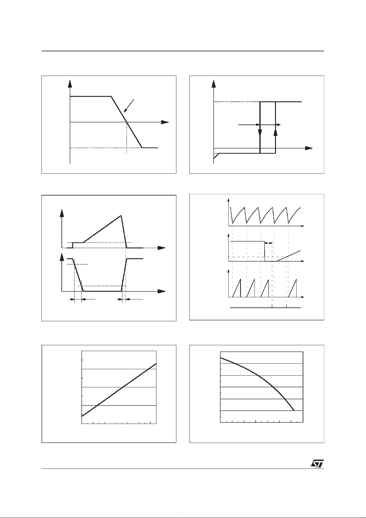
Figure1:VDDRegulationPoint
COMP
I
ICOMPHI
0
ICOMPLO
VDDreg
Figure3: TransitionTime
ID
10%Ipeak
Slope =
Gm in mA/V
FC00150
Figure2: UndervoltageLockout
IDD
IDD0
DD
V
VDDhyst
V
DDoff
IDDch
Figure4: ShutDown Action
VOSC
VCOMP
t
tDISsu
VDS=70V
Fsw = 0
V
DDon
FC00170
VDD
t
VDS
VCOMPth
90%VD
ID
10%V
D
t
tf tr
FC00160
ENABLE
DISABLE
Figure5: BreakdownVoltage vs Temperature Figure 6: Typical FrequencyVariation
1.15
BV
DS S
(Nor malize d)
1.1
1.05
0.95
1
0 20406080100120
Temperature ( C)
FC00180
1
(%)
0
-1
-2
-3
-4
-5
0 20 40 60 80 100 120 140
Temperature ( C)
t
t
ENABLE
FC00060
FC00190
6/20
Page 7

Figure7: Start-upWaveforms
VIPER100B/BSP
Figure8: OvertemperatureProtection
Ttsd
Tts d-Thys t
Vddon
Vddoff
Tj
t
Vdd
t
Id
t
Vco mp
t
SC1 019 1
7/20
Page 8

VIPER100B/BSP
Figure9: Oscillator
Ct
Rt
OSC
~360Ω
VDD
Dmax
0.9
0.8
0.7
For RT> 1.2 KΩ:
SW
MAX
=
= 1 −
R
2.3
TCT
R
D
MAX
550
− 150
T
MAX
values:
F
CLK
D
RecommendedD
100KHz: > 80%
200KHz: > 70%
FC00050
Maximum duty cycle vs Rt
1
FC00040
Frequency (kHz)
0.6
0.5
1 2 3 5 10 20 30 50
Rt (kΩ)
Oscillatorfrequency vs Rt and Ct
1,000
Ct = 1.5 nF
500
Ct = 2.7 nF
300
Ct = 4.7 nF
200
Ct = 10nF
100
50
30
1 2 3 5 10 20 30 50
Rt (kΩ)
FC00030FC00030
8/20
Page 9

Figure10: Error AmplifierFrequencyResponse
60
RCOMP= +∞
RCOMP= 270k
40
RCOMP= 82k
RCOMP= 27k
VIPER100B/BSP
FC00200
20
VoltageGain (dB)
RCOMP= 12k
0
(20)
0.001 0.01 0.1 1 10 100 1,000
Figure11: Error AmplifierPhase Response
200
150
Frequency (kHz)
FC00210
RCOMP= +∞
RCOMP= 270k
RCOMP= 82k
RCOMP= 27k
Phase (°)
100
50
RCOMP= 12k
0
(50)
0.001 0.01 0.1 1 10 100 1,000
Frequency (kHz)
9/20
Page 10

VIPER100B/BSP
Figure12: AvalancheTest Circuit
L1
1mH
BT2
12V
C1
47uF
16V
1
U1
VIPer100B
R2
1k
OSC
23
DRAINVDD
-
13V
+
COMP SOURCE
54
R3
100
Q1
2 x STHV102FI in parallel
R1
47
GENERATOR INPUT
500us PULSE
FC00195B
BT1
0 to 20V
10/20
Page 11

Figure13: Off Line Power Supply WithAuxiliarySupply Feedback
F1
BR1
D1
C2
C4
R1
D3
C3
R7
AC IN
TR2
C1
R9
TR1
VIPER100B/BSP
D2
C7
C10
L2
C9
+Vcc
GND
R2
13V
+
C11
OSC
C5
DRAINVDD
COMP SOURCE
C6
R3
Figure14: Off Line Power Supply With OptocouplerFeedback
F1
13V
BR1
+
C2
D3
C4
COMP SOURCE
D1
R1
C3
R7
DRAINVDD
VIPer100B
AC IN
TR2
C1
R9
R2
OSC
C5
VIPer100B
TR1
FC00081B
D2
C7
C10
L2
C9
+Vcc
GND
C11
C6
R3
R6
ISO1
R4
U2
C8
R5
FC00091B
11/20
Page 12

VIPER100B/BSP
OPERATIONDESCRIPTION:
CURRENT MODETOPOLOGY:
The current mode control method, like the one
integratedin the VIPer100B/BSPuses two control
loops - an inner current control loop and an outer
loop for voltage control. When the Power
MOSFET output transistor is on, the inductor
current (primary side of the transformer) is
monitored with a SenseFET technique and
converted into a voltage V
current. When V
reaches V
S
proportional to this
S
(the amplified
COMP
output voltage error) the power switch is switched
off. Thus, the outer voltage control loop defines
the level at which the inner loop regulates peak
current through the power switch and the primary
windingof the transformer.
Excellent open loop D.C. and dynamic line
regulation is ensured due to the inherent input
voltage feedforward characteristic of the current
mode control. This results in an improved line
regulation, instantaneous correction to line
changes and better stability for the voltage
regulationloop.
Current mode topology also ensures good
limitation in the case of short circuit. During a first
phase the output current increases slowly
followingthe dynamic of the regulation loop. Then
it reaches the maximum limitation current
internally set and finally stops because thepower
supply on V
is no longer correct. For specific
DD
applications the maximum peak current internally
set can be overridden by externally limiting the
voltage excursion on the COMP pin. An
integrated blanking filter inhibits the PWM
comparator output for a short time after the
integrated Power MOSFET is switched on. This
function prevents anomalous or premature
termination of the switching pulse in the case of
current spikes caused by primary side
capacitance or secondary side rectifier reverse
recovery time.
STAND-BY MODE
Stand-by operation in nearly open load condition
automatically leads to a burst mode operation
allowing voltage regulation on the secondary
side. The transition from normal operation to
burst mode operation happens for a power P
STBY
given by :
1
2
P
STBY
L
=
PISTBY
2
F
SW
Where:
L
isthe primary inductanceof the transformer.
P
F
is the normal switching frequency.
SW
I
is the minimum controllable current,
STBY
corresponding to the minimum on time that the
deviceis able to provide in normal operation.This
current can be computedas :
I
STBY
b
=
IN
L
P
+ td) V
(t
tb+tdis the sum of the blanking time and of the
propagation time of the internal current sense
and comparator, and represents roughly the
minimum on time of the device. Note that P
STBY
may be affected by the efficiencyof the converter
at low load, and mustinclude the power drawn on
the primary auxiliaryvoltage.
As soon as the power goes below this limit, the
auxiliary secondary voltage starts to increase
above the 13V regulation level forcing the output
voltage of the transconductance amplifier to low
state (V
COMP
<V
). This situation leads to
COMPth
the shutdown mode where the power switch is
maintained in the off state, resulting in missing
cycles and zero duty cycle. As soon as V
back to the regulation level and the V
gets
DD
COMPth
threshold is reached, the device operates again.
The above cycle repeats indefinitely, providing a
burst mode of which the effective duty cycle is
much lower than the minimum one when in
normal operation. The equivalent switching
frequency is also lower than the normal one,
leading to a reduced consumption on the input
mains lines. This mode of operation allows the
VIPer100B/BSP to meet the new German ”Blue
Angel” Norm with less than 1W total power
consumption for the system when working in
stand-by. The output voltage remains regulated
around the normal level, with a low frequency
ripple corresponding to the burst mode. The
amplitude of this ripple is low, because of the
output capacitors and of the low output current
drawn in such conditions.The normal operation
resumes automatically when the power get back
to higher levels than P
STBY
.
HIGH VOLTAGE START-UP CURRENT
SOURCE
An integrated high voltage current source
provides a bias current from the DRAIN pin
during the start-up phase. This current is partially
absorbed by internal control circuits which are
12/20
Page 13

VIPER100B/BSP
placed into a standby mode with reduced
consumption and also provided to the external
capacitor connected to the V
pin. As soon as
DD
the voltage on this pin reaches the high voltage
threshold V
of the UVLO logic, the device
DDon
turns into active mode and starts switching. The
start up current generatoris switched off, and the
converter should normally provide the needed
current on the V
pin through the auxiliary
DD
winding of the transformer, as shown on figure
15.
In case of abnormal condition where the auxiliary
winding is unable to provide the low voltage
supply current to the V
pin (i.e. short circuit on
DD
the output of the converter), the external
capacitor discharges itself down to the low
threshold voltage V
of the UVLO logic, and
DDoff
the device get back to the inactive state where
the internal circuits are in standby mode and the
start up current source is activated. The converter
enters a endless start up cycle, with a start-up
duty cycle defined by the ratio of charging current
towards discharging when the VIPer100B/BSP
tries to start. This ratio is fixed by design to 2 to
15, which gives a 12% start up duty cycle while
the power dissipation at start up is approximately
0.6 W, for a 230 Vrms input voltage. This low
value of start-up duty cycle preventsthe stress of
the output rectifiers and of the transformer when
in short circuit.
The external capacitor C
on the VDDpin must
VDD
be sized according to the time needed by the
converter to start up, when the device starts
switching. This time t
depends on many
SS
parameters, among which transformer design,
output capacitors, soft start feature and
compensation network implemented on the
COMP pin. The following formula can be used for
definingthe minimum capacitor needed:
I
>
DDtSS
V
DDhyst
C
VDD
where:
I
is the consumption current on the VDDpin
DD
when switching. Refer to specified I
DD1
and I
DD2
values.
t
is the start up time of the converter when the
SS
device begins to switch. Worst case is generally
at full load.
V
DDhyst
is the voltage hysteresis of the UVLO
logic. Refer to the minimum specified value.
Soft start feature can be implemented on the
COMP pin through a simple capacitor which will
be also used as the compensation network. In
this case, the regulation loop bandwidth is rather
low, because of the large value of this capacitor.
In case a large regulation loop bandwidth is
mandatory, the schematics of figure 16 can be
Figure15: Behaviourof the high voltagecurrent source at start-up
windin g
2mA
15 mA
C
VDD
VDD
15 mA1mA
Ref.
UNDERVOLTAGE
LOCKOUT LOGIC
VDD
VDDon
VDDoff
t
Auxiliary prima ry
VIP er 1 0 0B
Start up duty cycle ~ 10%
3mA
DRAIN
SOURCE
FC00100B
13/20
Page 14

VIPER100B/BSP
used. It mixes a high performance compensation
network together with a separate high value soft
start capacitor. Both soft start time and regulation
loop bandwidth can be adjustedseparately.
If the device is intentionally shut down by putting
the COMP pin to ground, the device is also
performingstart-up cycles, and the V
oscillatingbetween V
DDon
and V
DDoff
voltage is
DD
. This voltage
can be used for supplying external functions,
provided that their consumption doesn’t exceed
0.5mA. Figure 17 shows a typical application of
this function, with a latched shut down. Once the
”Shutdown” signal has been activated, the device
remains in the off state until the input voltage is
removed.
TRANSCONDUCTANCE ERROR AMPLIFIER
The VIPer100B/BSPincludesa transconductance
error amplifier. Transconductance Gm is the
change in output current (I
in input voltage(V
I
∂
COMP
=
G
m
∂ V
DD
The output impedanceZ
). Thus:
DD
COMP
) versus change
COMP
at the output of this
amplifier(COMP pin) can be definedas:
Z
COMP
∂V
COMP
=
∂ I
=
COMP
G
∂ V
1
m
COMP
x
∂ V
DD
This last equation shows that the open loop gain
A
canbe related to GmandZ
VOL
A
VOL=GmxZCOMP
COMP
:
where Gmvalue for VIPer100B/BSP is 1.5 mA/V
typically.
G
is well defined by specification, but Z
m
and therefore A
are subject to large
VOL
COMP
tolerances. An impedance Z can be connected
between the COMP pin and ground in order to
define more accurately the transfer function F of
the error amplifier, according to the following
equation,very similar to the one above:
F
=Gm x Z(S)
(S)
The error amplifier frequency response is
reported in figure 10 for different values of a
simple resistance connected on the COMP pin.
The unloaded transconductance error amplifier
shows an internal Z
of about 330 KΩ. More
COMP
complex impedance can be connected on the
COMP pin to achieve different compensation
laws. A capacitor will provide an integrator
function, thus eliminating the DC static error, and
a resistance in series leads to a flat gain at higher
frequency, insuring a correct phase margin. This
configurationis illustrated on figure 18.
As shown in figure 18 an additional noise filtering
capacitor of 2.2 nF is generally needed to avoid
any highfrequencyinterference.
It can be also interesting to implement a slope
compensation when working in continuous mode
with duty cycle higher than 50%. Figure 19 shows
such a configuration. Note that R1 and C2 build
the classical compensation network, and Q1 is
injecting the slope compensation with the correct
polarity from the oscillator sawtooth.
EXTERNALCLOCK SYNCHRONIZATION:
The OSC pin provides a synchronisation
capability, when connected to an external
Figure16: MixedSoft Start and Compensation
D2
+
14/20
VIPer100B
-
OSC
13V
+
C4
C3
DRAINVDD
COMP SOURCE
R1
C1
D1
C2
+
D3
R3
R2
FC00131B
AUXILIARY
WINDING
Figure17: Latched Shut Down
R1
Q2
R4
Shutdown Q1
OSC
13V
R2R3
D1
VIPer100B
-
+
FC00110B
DRAINVDD
COMP SOURCE
Page 15

VIPER100B/BSP
frequency source. Figure 20 shows one possible
schematic to be adapted depending the specific
needs. If the proposed schematic is used, the
pulse duration must be kept at a low value (500ns
is sufficient) for minimizing consumption. The
optocoupler must be able to provide 20mA
through the optotransistor.
PRIMARY PEAK CURRENT LIMITATION
The primary I
DPEAK
current and, as resulting
effect, the output power can be limited using the
simple circuit shown in figure 21. The circuit
based on Q1, R
and R2clamps the voltage on
1
the COMP pin in order to limit the primary peak
current of the device to a value:
Figure18: TypicalCompensation Network
VIPer100B
DRAINVDD
COMP SOURCE
R1
C1
OSC
13V
-
+
C2
I
DPEAK
V
=
COMP
H
− 0.5
ID
where:
+ R
R
1
V
COMP
= 0.6 x
2
R
2
The suggestedvalue for R1+R2is in the range of
220KΩ.
OVER-TEMPERATURE PROTECTION:
Over-temperature protection is based on chip
temperature sensing. The minimum junction
temperature at which over-temperature cut-out
occurs is 140
o
C while the typical value is 170oC.
The device is automatically restarted when the
junction temperature decreases to the restart
temperaturethreshold thatis typically40
o
C below
Figure19: SlopeCompensation
R1R2
OSC
Q1
VIPer100B
-
13V
+
C2
DRAINVDD
COMP SOURCE
C3
C1 R3
FC00121B
FC00141B
Figure20:ExternalClock Synchronization Figure21:Current LimitationCircuit Example
VIPer100B
DRAINVDD
COMP SOURCE
Q1
FC00240B
10 kΩ
OSC
13V
VIPer100B
+
COMP SOURCE
FC00220B
13V
-
+
R1
R2
OSC
DRAINVDD
15/20
Page 16

VIPER100B/BSP
Figure22: Recommendedlayout
Frominput
diodes bridge
R1
C1
C2
1
OSC
U1
VIPer100B
2
-
+
13V
ISO1
COMP SOURCE
R2
C3
C4
LAYOUTCONSIDERATIONS
Some simple rules insure a correct running of
switching power supplies. They may be classified
into two categories:
- To minimisepowerloops: the way the switched
power current must be carefully analysed and
the corresponding paths must present the
smallest inner loop area as possible. This
avoids radiated EMC noises, conducted EMC
noises by magnetic coupling, and provides a
better efficiency by eliminating parasitic
inductances,especially on secondaryside.
- Touse different tracksfor low level signals and
T1
D2
3
DRAINVDD
C5
5
4
D1
To secondary
C7
filteringandload
C6
FC00500B
power ones. The interferences due to a mixing
of signal and power may result in instabilities
and/or anomalous behaviour of the device in
case of violent power surge (Input
overvoltages,output short circuits...).
In case of VIPer, these rules apply as shown on
figure 22. The loops C1-T1-U1, C5-D2-T1,
C7-D1-T1 must be minimised. C6 must be as
close as possible from T1. The signal
components C2, ISO1, C3 and C4 are using a
dedicated track to be connected directly to the
sourceof the device.
16/20
Page 17

PENTAWATT HV (VERTICAL) MECHANICAL DATA
VIPER100B/BSP
DIM.
MIN. TYP. MAX. MIN. TYP. MAX.
mm inch
A 4.30 4.80 0.169 0.189
C 1.17 1.37 0.046 0.054
D 2.40 2.80 0.094 0.110
E 0.35 0.55 0.014 0.022
F 0.60 0.80 0.024 0.031
G1 4.90 5.28 0.193 0.208
G2 7.42 7.82 0.292 0.308
H1 9.30 9.70 0.366 0.382
H2 10.40 0.409
H3 10.05 10.40 0.396 0.409
L 16.60 17.30 0.653 0.681
L1 14.60 15.22 0.575 0.599
L2 21.20 21.85 0.835 0.860
L3 22.20 22.82 0.874 0.898
L5 2.60 3.00 0.102 0.118
L6 15.10 15.80 0.594 0.622
L7 6.00 6.60 0.236 0.260
M 2.50 3.10 0.098 0.122
M1 7.56 8.16 0.298 0.321
R 0.50 0.020
V4 90
o
90
Diam. 3.70 3.90 0.146 0.154
G2
G1
M1
M
leads
E
Resin
between
V4
F
L
L1
A
L5
H1
C
H3
H2
Diam
P023H3
R
D
L6
L7
L2
L3
17/20
Page 18

VIPER100B/BSP
PENTAWATT HV 022Y(VERTICAL HIGH PITCH) MECHANICAL DATA
DIM.
MIN. TYP. MAX. MIN. TYP. MAX.
mm inch
A 4.30 4.80 0.169 0.189
C 1.17 1.37 0.046 0.054
D 2.40 2.80 0.094 0.110
E 0.35 0.55 0.014 0.022
F 0.60 0.80 0.024 0.031
G1 4.90 5.28 0.193 0.208
G2 7.42 7.82 0.292 0.308
H1 9.30 9.70 0.366 0.382
H2 10.40 0.409
H3 10.05 10.40 0.396 0.409
L 16.42 17.42 0.646 0.686
L1 14.60 15.22 0.575 0.599
L3 20.52 21.52 0.808 0.847
L5 2.60 3.00 0.102 0.118
L6 15.10 15.80 0.594 0.622
L7 6.00 6.60 0.236 0.260
M 2.50 3.10 0.098 0.122
M1 5.00 5.70 0.197 0.224
R 0.50 0.020
V4 90
o
90
o
Diam. 3.70 3.90 0.146 0.154
G2
M1
G1
M
leads
E
Resin
between
F
L
L1
A
R
V4
D
L6
L7
L3
L5
H1
C
H3
H2
Diam
P023H2
18/20
Page 19

PowerSO-10 MECHANICAL DATA
VIPER100B/BSP
DIM.
MIN. TYP. MAX. MIN. TYP. MAX.
mm inch
A 3.35 3.65 0.132 0.144
A1 0.00 0.10 0.000 0.004
B 0.40 0.60 0.016 0.024
C 0.35 0.55 0.013 0.022
D 9.40 9.60 0.370 0.378
D1 7.40 7.60 0.291 0.300
e 1.27 0.050
E 9.30 9.50 0.366 0.374
E1 7.20 7.40 0.283 0.291
E2 7.20 7.60 0.283 0.300
E3 6.10 6.35 0.240 0.250
E4 5.90 6.10 0.232 0.240
F 1.25 1.35 0.049 0.053
h 0.50 0.002
H 13.80 14.40 0.543 0.567
L 1.20 1.80 0.047 0.071
q 1.70 0.067
α 0
o
o
8
==
==
HE
h
A
F
A1
610
51
eB
M
0.25
D
==
D1
==
E2
==
DETAIL”A”
DETAIL”A”
Q
B
0.10 A
E1E3
==
SEATING
PLANE
A
C
α
B
E4
==
SEATING
PLANE
A1
L
==
0068039-C
19/20
Page 20

VIPER100B/BSP
Information furnished is believed to beaccurate and reliable. However, STMicroelectronics assumes no responsibility for the consequences
of use of such information nor for any infringement of patents or other rights of third parties which may result from its use. No license is
granted by implication or otherwise under any patent or patent rights of STMicroelectronics. Specification mentioned in this publication are
subject to change without notice. This publication supersedes and replaces all information previously supplied. STMicroelectronics products
are not authorized for use as critical components in life support devices or systems without express written approval of STMicroelectronics.
The ST logo is a trademark of STMicroelectronics
2000 STMicroelectronics – Printed in Italy – All Rights Reserved
STMicroelectronicsGROUP OF COMPANIES
Australia - Brazil - China - Finland - France - Germany - Hong Kong - India - Italy - Japan - Malaysia - Malta - Morocco -
Singapore- Spain - Sweden - Switzerland -United Kingdom - U.S.A.
http://www.st.com
20/20
 Loading...