

Datasheet VIC068A-UMB, VIC068A-UM, VIC068A-NC, VIC068A-GMB, VIC068A-GI Datasheet (Cypress)
...Page 1

VMEbus Interface Controller
VIC068A
1VIC068A
Features
Complete VMEbus interface controller and arbiter
—58 internal registers provide c onfigur ation control
and status of VMEbus and local operations
—Drives arbitration, interrupt, address modifier utility,
strobe, address lines A07through A01 and data lines
D07 through D00 directly, and provides signals for
control logic to drive remaining address and data
line s
—Direct connection to 68xxx family and mappable to
non-68xxx processors
• Complete master/slave capability
—Supports read, write, write posting, and block trans-
fers
—Accommodates VMEbus timing requirements with
internal digital delay line (
—Programmable metastability delay
—Programmable data acquisition delays
—Provides timeout timers for local bus and VMEbus
transactions
• Interleaved block transfers over VMEbus
—Acts as DMA master on lo cal bus
—Programmable burst count, t ransfer length, and in-
terleaved period interval
— Supports local module-based DMA
• Arbitration support
—Supports single-level, priority and round robin arbi-
tration
—Supports fair request option as
requester
• Interrupt support
—Complete support for the VMEbus interrupts: inter-
rupter and interr upt handler
1
⁄2-clock granularity)
—Seven local interrupt lines
—8-level interrupt priority encode
—Total of 29 interrupts mapped through the VIC068A
• Miscellaneous features
—Refresh option for local DRAM
—Four broadcast location monitors
—Four module-specific location
monitor s
—Eight interprocessor communications registers
—PGA or QFP packages
—Compatible with IEEE Specification 1014, Rev. C
—Supports RMC operations
• See the
mation
VIC068A/V AC068A User’s Guide
for more infor-
Functional Description
The VMEbus interface controller (VIC068A) is a single chip
designed to minimize the cost and board area requirements
and to maximize performance of the VMEbus interface of a
VMEbus master/slave module. This can be implemented on
VIC068Aeither a 8-bit, 16-bit , or 32-bit VMEbus system. Th e
VIC068A performs all VMEbus system controller functions
plus many others, which simplify the development of
VIC068Aa VMEbus interface. The VIC068A utilizes patented
on-chip output buffers. These CMOS high-drive buffers provide direct connection to the address and data lines. In addition to these signals, the VIC068A connects directly to the arbitration, interrupt, address modifier, utility and strobe lines.
Signals are provided which control data direction and latch
functions needed for a 32-bit implementation.
The VIC068A was developed through the efforts of a consortium of board vendors, under the auspices of the VMEbus International Trade Association (VITA). The VIC068A thus insures compatibility between boards designed by different
manufacturers.
Cypress Semiconductor Corporation • 3901 North First Street • San Jose • CA 95134 • 408-943-2600
December 1990 – Revised April 1995
Page 2
VIC068A
Pin Configurations
Pin Grid Array (PGA)
Bottom View
AB CDE FG HJ KL MN P R
GND
LD6
LD2
LD1
LA7
LA3
LA2
LA1
CS*
IPL2*
BLT*
LD5
LD3
LD0
LA5
LA4
LA0
DSACK1*
LIACKO*
IPL1*
DEDLK*
LD7
LD4
LA6
GND
VCC
DS*
LIRQ2*
VCC
IPL0*
LOCATOR
PIN
LIRQ5*
LIRQ1*
LAEN
ASIZ1
LIRQ4*
LIRQ3*
ASIZ0
LIRQ6*
LIRQ7*
SLSEL1*
ICFSEL*
GND
WORD*
MWB*
SLSEL0*
FIACK*
A01
GND
A02
A03
A06
A04
A05
IRQ1*
VCC
A07
IRQ2*
IRQ5*
SYSFAIL*
IACKIN*
GND
GND
VCC
GND
IRQ3*
IRQ6*
VCC
SYSRESET*
IACK*
AS*
AM2
LWORD*
IRQ4*
IRQ7*
ACFAIL*
IACKOUT*
DTACK*
AM0
AM1
AM3
AM4
PAS*
DSACK0*
HALT*
FC2
SIZ1
LBG*
LBERR*
R/W*
RMC*
SIZ0
IRESET*
ABEN*
RESET*
FC1
LBR*
SCON*
LADO
VCC
CLK64M
LEDI
LEDO
LADI
DDIR
UWDENIN*
GND
LWDENIN*
SWDEN*
VCC
DENO*
ISOBE*
GND
D06
D07
VCC
D03
D05
D00
D01
D04
BGOUT1*
GND
D02
BGIN2*
BGOUT0*
BGOUT3*
BERR*
BR2*
BBSY*
BGIN0*
BGIN3*
BGOUT2*
WRITE*
DS1*
BR1*
BR3*
BGIN1*
SYSCLK
AM5
DS0*
BR0*
GND
BCLR*
GND
VIC068A–1
2
Page 3
Pin Configurations (continued)
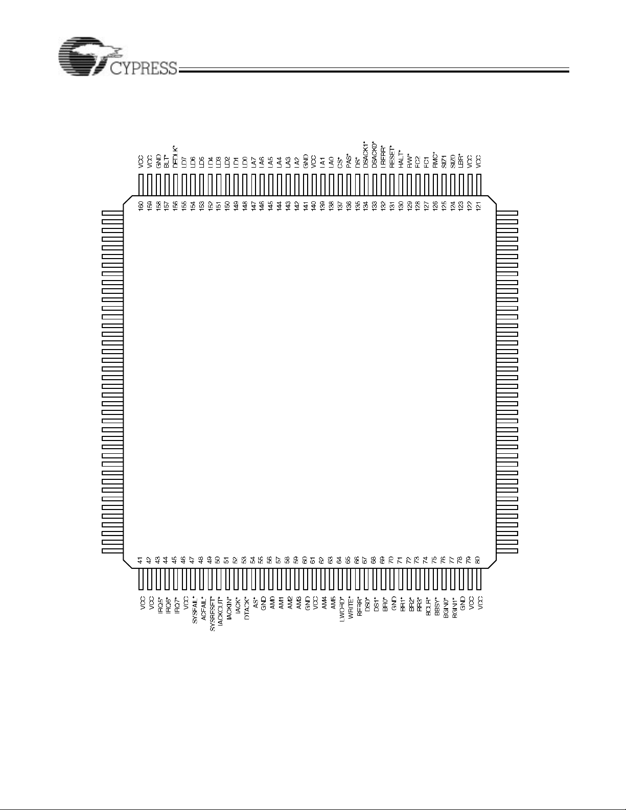
1GND 120 GND
2GND 119 GND
3IPL0* 118 LBG*
4IPL1* 117 IRESET*
5IPL2* 116 SCON*
6VCC 115 CLK64M
7LAEN 114 ABEN*
8LIAKO* 113 LADO
9LIRQ1* 112 LADI
10LIRQ2* 111 LEDI
11LIRQ3* 110 VCC
12LIRQ4* 109 LEDO
13LIRQ5* 108 DDIR
14LIRQ6* 107 UWDENIN*
15LIRQ7* 106 GND
16ASIZ1* 105 LWDENIN*
17ASIZ0* 104 DENO*
18ICFSEL* 103 SWDEN*
19SLSEL1* 102 ISOBE*
20GND 101 VCC
21SLSEL0* 100 GND
22WORD* 99 D07
23FCIACK* 98 D06
24MWB* 97 D05
25A1 96 D04
26GND 95 VCC
27A2 94 D03
28A3 93 D02
29A4 92 D01
30VCC 91 D00
31A5 90 BGOUT3*
32A6 89 GND
33A7 88 BGOUT2*
34VSS 87 BGOUT1*
35IRQ1* 86 BGOUT0*
36IRQ2* 85 SYSCLK
37IRQ3* 84 BGIN3*
38IRQ4* 83 BGIN2*
39GND 82 GND
40GND 81 GND
VIC068A
160-Pin QuadFlatpack (QFP)
Top View
VIC068A–2
3
Page 4
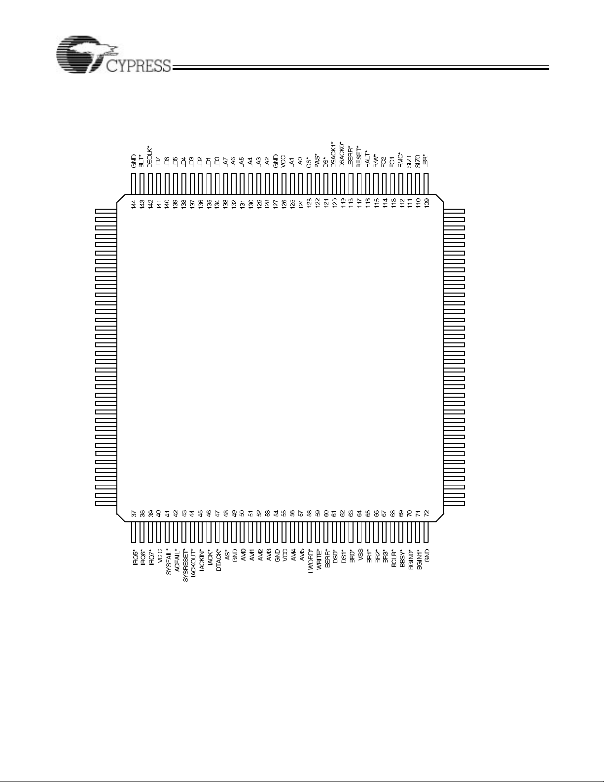
Pin Configurations (continued)
VIC068A
144-Pin Thin Quad Flatpack (TQFP)
TopView
IPL1* IRESET*
IPL2* SCON*
VCC CLK64M
LAEN ABEN*
LIAKO* LADO
LIRQ1* LADI
LIRQ2* LEDI
LIRQ3* VCC
LIRQ4* LEDO
LIRQ5*
LIRQ6*
LIRQ7*
ASIZ1*
ASIZ0*
ICFSEL*
SLSEL1*
GND
SLSEL0*
WORD*
FCIACK*
MWB*
A1
GND
A2
A3
A4
VCC
A5
A6
A7
GND
IRQ1*
IRQ2*
IRQ3*
IRQ4*
1
2
3
4
5
6
7
8
9
10
11
12
13
14
15
16
17
18
19
20
21
22
23
24
25
26
27
28
29
30
31
32
33
34
35
36
108
107
106
105
104
103
102
101
100
99
98
97
96
95
94
93
92
91
90
89
88
87
86
85
84
83
82
81
80
79
78
77
76
75
74
73
LBG*IPL0*
DDIR
UWDENIN*
GND
LWDENIN*
DENO*
SWDEN*
ISOBE*
VCC
GND
D07
D06
D05
D04
VCC
D03
D02
D01
D00
BGOUT3*
GND
BGOUT2*
BGOUT1*
BGOUT0*
SYSCLK
BGIN3*
BGIN2*
VIC068A–3
4
Page 5

VIC068A on 68030 Board
512/256K X 36 DRAM 512/256K X 36 DRAM
VIC068A
68030
32
Latching Transceivers
LD0 –LD31
LA0 –LA31
Map Decoder
DRAM I/O
FCT
245
Address
Mux
EPROM
VMEbus
MWB*
WORD*
ASIZ1
ASIZ0
32
Latching Transceivers
4 JEDEC EPROMs
FCT
543
FCT
543
FCT
245
Parity Check
Logic
D24–D31
D16–D23
FCT
245
FCT
245
FCT
543
A31–A24 A23–16 A15–A08
FCT
543
FCT
543
ISOBE*
W1
Slave
Select
Decode
LD0 –LD7
LA0 –LA7
SCON*
SLSEL0*
SLSEL1*
ICFSEL
VIC068A
LIRQ1* - LIRQ7*LIACKO*
FCT
543
D08–D16
A1 – A 7
SYSCLK
D00 –D07
AM0 – AM5
AS*, DS0*, DS1*, DTACK*,
WRITE*, LWORD*, BERR*
BGiIN*, BGiOUT*, BRi*, BBSY*
IACK*, IACKIN*, IACKOUT*
IRQ1*, IRQ7*, ACFAIL*,
SYSFAIL*
STSRESET*
VIC068A–4
5
Page 6

VIC068A
Theory of Operation
The VIC068A is an interface between a local CPU bus and the
VMEbus. The local bus interface of the VIC068A emulates Motorola’s family of 32-bit CISC processor interfaces. Other processors can easily be adapted to interface to the VIC068A
using the appropriate logic.
Resetting the VIC068A
The VIC068A can be reset by any of three distinct reset conditions:
Internal Reset. This re set is the most common m eans of r esetting the VIC068A. It resets select register v alues and all
logic within the device.
System Reset. This reset provides a means of resetting the
VIC068A through the VMEbus backplane. The VIC068A may
also signal a SYSRESET* by writing a configuration register.
Global Reset. This provides a complete reset of the VIC068A.
This reset resets all of t h e VIC068A’s c onfigurati o n r e gisters.
This reset should be used with caution since SYSCLK is not
driven while a global reset is in progress.
All three reset options are implemented in a di fferent manner
and have different effects on the VIC068A configuration registers.
VIC068A VMEbus System Controller
The VIC068A is capable of operating as the VMEbus system
controller. It provides VMEbus arbitration functions, including:
• Priority, round-robin, and single-level arbitrati on schemes
• Driving IACK* Daisy-Chain
• Driving BGiOUT* Daisy-Chain (All four levels)
• Driving SYSCLK output
• VMEbus arbitration timeout timer
The System controller functions are enabled by the SCON* pin
of the VIC068A. When strapped LOW, the VIC068A functions
as the VMEbus system controller.
VIC068A VMEbus Master Cycles
The VIC068A is capable of becoming the VMEbus master in
response to a request from local resources. In this situation,
the local resource requests that a VMEbus transfer is desired.
The VIC068A makes a request for the VMEbus. When the
VMEbus is g ranted to the VIC068A, i t then performs the transfer and acknowledges the local resource and the cycle is complete. The VIC068A is cap able o f al l four VMEbus re quest levels. The following release modes are supported:
• Release on request (ROR)
• Release when done (RWD)
• Release on clear (ROC)
• Release under RMC* control
• Bus capture and hold (BCAP)
The VIC068A supports A32, A24, and A16, as well as user-defined address spaces.
Master Write-Posting
The VIC068A is capable of performing master write-posting
(bus decoupling). In this situation, the VIC068A acknowledges
the local resource
VIC068A is made, thus freeing the local bus. The VIC068A
immediately
after the request to the
latches the local data to be written and performs the VMEbus
transfer without the local resource having to wait for VMEbus
arbitration.
Indivisible Cycles
Read-modify-write cycles and indivisible multiple- address cycles (EMACS) are easily performed using t he VIC068A. Significant control is allowed to:
• Requesting the VMEbus on the assertion of RMC* independent of MWB* (this prevents any slave access from interrupting local indivisible cycles)
• Stretching the VMEbus AS*
• Making the above behavi ors depe ndent on t he local SIZi si gnals
Deadlock Condition
If a master operation is attempted when a slave operation to
the same module is in progress, a deadlock condition has occurred. The VIC068A will signal a deadlock condition by asserting the DEDLK* signal. This should be used by the local
resource requesting the VMEbus to try the transfer after the
slave access has completed.
Self-Access Condition
If the VIC068A, while it is VMEbus master, has a slave select
signaled, a self access i s said to h ave o ccurred. The VIC068A
will issue a BERR*, which in turn will cause a LBERR* to be
asserted.
VIC068A VMEbus Slave Cycles
The VIC068A is capable of operating as a VMEbus slave co ntroller. The VIC068A contains a h ighly programmable environment to allow for a wide variety of sl ave configurations. The
VIC068A allows for:
• D32, D16, or D8 configuration
• A32, A 24, A16, or user-defined address spaces
• Pr ogrammable block transfer support including:
— DMA-type blo ck tra ns fer (PAS* and DSACK i* held
assert ed )
— non-DMA-t ype bl o ck t ran sf er (to gg le PAS* and DSAC Ki* )
— No support for block transfer
• Pr ogrammable data acquisition delays
• Pr ogrammable PAS* and DS* timing
• Restricted slave accesses (supervisory accesses only)
When a s lav e access is required, the VIC068A will request the
local bus. When local bus mastership is obtained, the
VIC068A will read or write the data to/from the lo cal resource
and assert the DTACK* signal to complete the transfer.
Slave Write-Posting
The VIC068A is capable of performing a slave write-post operation (bus decoupling). When enab led, the VIC068A latches
the data to be written and acknowledge the VMEbus (asserts
DTACK*) immediately th ereafter. This prevents the VMEbus
from having to wait for local bus access.
Address Modifier (AM) Codes
The VIC068A encodes and decodes the VMEbus address
modifier codes. For VMEbus master accesses, the VIC068A
encodes the appropriate AM codes through the VIC068A FCi
and ASIZi signals, as well as the block transfer status. For
6
Page 7

VIC068A
slave accesses, the VIC068A decodes the AM codes and
checks the slave select control registers t o see if the slave
request is to be supported with regard to address spaces, supervisory accesses, and block transfers. The VIC068A also
supports user-defined AM codes; that is, the VIC068A can be
made to assert and respond to user-defined AM codes.
VIC068A VMEbus Block Transfers
The VIC068A is capable of bo th master an d slave block transfers. The master VIC068A performs a block transfer in one of
two modes:
• MOVEM-type Block Transfer
• Master Block Transfer with Local DMA
In addition to these VMEbus block transfers, the VIC068A is
also capable of performing block transfers from one local resource to another in a DMA-like fashion. This is referred to as
a Module-based DMA transfer.
The VMEbus s pecification restricts block t ransfers f rom crossing 256-byte boundaries without toggling the address strobe,
in addition to restricting the maximum length of the transfer to
256 bytes. The VIC068A allows for easy implementation of
block transfers that exceed the 256-byte restriction by releasing the VMEbus at the appropriate time and rearbit rating for
the bus at a programmed time later (this i n-between time is
referred to as the interleave period), while at the same time
holding both the local and VMEbus addresses with internal
latches. All of this is performed without processor/software intervention until the transfer is complete.
The VIC068A contains two separate address counters for the
VMEbus and the local address buses. In addition, a separate
address is counter-provided for slave block transfers. The
VIC068A address counters are 8-bit up-counter s that provide
for transfers up to 256 bytes. For transfers that exceed the
256-byte limit, the Cypress CY7C964 or externa l counters and
latches are required.
The VIC068A allows slave accesses to occur during the interleave period. Master accesses are also allowed during interleave with programming and external logic. This is referred to
as the “dual path” option.
MOVEM Master Block Transfer
This mode of block transfer provides the simplest implementation of VMEbus block transfers. For this mode, the local resource simply configures the VIC068A for a MOVEM block
transfer and proceeds with the consecutive-address cycles
(such as a 680X0 MOVEM instruction). The local resource
continues as the local bus master in this mode.
Master Block Transfers with Local DMA
In this mode, the VIC068A becomes the local bus master and
reads or writes the local data in a DMA-like fashion. This provides a much faster interface than the MOVEM block transfer,
but with less control and fault tolerance.
VIC068A Slave Block Transfer
The process of receiving a block transfer is referre d to as a
slave block transfer. The VIC068A is capable of decoding the
address modifier codes to determine th at a slave block transfer is desired. In this mode, the VIC068A captures the VMEbus
address, and latches them into internal counters. For subsequent cycles, the VIC068A simply increments this counter for
each transfer. The local protocol for slave block transfers can
be configured in a full handshake mode by toggling both P AS*
and DS* and expecting DSACKi* to toggle, or in an accelerated mode in which only DS* toggles and PAS* is asserted
throughout the cycle.
Module-Based DMA Transfers
The VIC068A is capable of acting as a DMA controller between two local resources. This mode is similar to that of master block transfers with local DMA, with the exception that the
VMEbus is not the second source or destination.
VIC068A Interrupt Generation and Handling F acilities
The VIC068A is capable of generating and handling a seven-level prioritized interrupt scheme similar to that used by the
Motorola CISC processors. Th ese in terru pts include the seven
VMEbus interrupts, seven local interrupts, five VIC068A error/status interrupts, and eight interprocessor communication
interrupt s.
The VIC068A can be configured to act as handler for any of
the seven VMEbus interrupts. The VIC068A can generate the
seven VMEbus interrupts as well as supplying a user- defined
status/ID vector. The local p riority level (IPL) for VMEbus interrupts is programmable. When configured as the system controller, the VIC068 will drive the IACK daisy-chain.
The local interrupts can be configured with the following:
• User-defined local interrupt priority level ( IPL)
• Option for VIC068A to provide the status/ID vector
• Edge or level sensitivity
• Polar ity (risi ng/fall ing edge, active HIGH/LOW)
The VIC068A is also capable of generating local interrupts on
certain error or status conditions. These include:
• A C FAIL* asserte d
• SYSFAIL* asserted
• Fail ed master write-post (BERR* asserted)
• Local DMA completion for block transfers
• Arbitration timeout
• VMEbus interrupter interrupt
The VIC068A can also interrupt on the setting of a module or
global switch in the interprocessor communication facilities.
Interprocessor Communication Facilities
The VIC068A includes interprocessor registers and switches
that can be written and read through VMEbus accesses.
These are the only such registers that are directly ac cessible
from the VMEbus. Included in the interprocessor communication facilities are:
• Four general purpose 8-bit registers
• Four mo dule switches
• Four glo bal switches
• VI C0 68A version/revision register (read-only)
• VI C0 68A Reset/Halt condition (read-only)
• VI C0 68A interprocessor communication register semaphores
When set through a VMEbus access, these switches can interrupt a local resource. The VIC068A includes module switches that are intended for a single module, and global switches
which are intended to be used as a broadcast.
7
Page 8

VIC068A
Buffer Control Signal for Shared Memory Implementation
'245
B
A
EN
D32 CPU
D32 SHARED
MEMORY
D16
SHARED
MEMORY
DDIR
1=A to B
0=B to A
AB
'245
EN
SWDEN*
LD0 –LD15
ISOBE*
[1]
LEDI
LAEN
LA8– LA31
LWDENIN*
LADI
UWDENIN*
LD16 –LD31
LD6 –D15
CEBA*
LEBA*
OEBA*
A
CEBA*
LEBA*
OEBA*
A
CEBA*
LEBA*
OEBA*
A
'543
LE
Q
D
VMEbusA8 –A31
D
LE
B
Q
OEAB*
LEAB*
CEAB*
ABEN*
LADO
'543
LE
Q
D
VMEbusD16 –D31
D
LE
B
Q
OEAB*
LEAB*
CEAB*
'543
LE
Q
D
D
LE
B
Q
OEAB*
LEAB*
CEAB*
VMEbus
D8 –D15
DENO*
LEDO
LD0 –LD7
LA0–LA7
DSACK1*
DSACK0*
S1Z1
S1Z0
WORD*
VIC
LWORD*
VMEbusD00 –D07
VMEbusA01 –A07
DS0*
DS1*
Note:
1. This configuration can support Slave Block Transfers and Master and Slave Write-Post Operation. This buffer configuration cannot support block transfers with DMA.
Operating Range
Ambient
Range
Temperature
V
CC
Commercial 0°C to +70°C 5V ± 5%
Industrial –40°C to +85°C 5V ± 10%
Military –55°C to +125°C 5V ± 10%
Related Documents
VIC068A/VAC068A User’s Guide
VIC64/CY7C964 Design Notes
8
Page 9

Ordering Info rma tio n
VIC068A
Ordering Code
VIC068A-AC A144 144-Pin Thin Quad Flatpack Commercial
VIC068A-BC B144 145-Pin Plastic Pin Grid Array
VIC068A-GC G145 145-Pin Ceramic Pin Grid Array
VIC068A-NC N160 160-Lead Plastic Quad Flatpack
VIC068A-GI G145 145-Pin Ceramic Pin Grid Array Industrial
VIC068A-GMB G145 145-Pin Ceramic Pin Grid Array MIL-STD-883
VIC068A-UM U162 160-Lead Ceramic Quad Flatpack Military Temp. Commercial
VIC068A-UMB U162 160-Lead Ceramic Quad Flatpack MIL-STD-883
Document #: 38-00167-C
Package
Name Package Type
Operating
Range
9
Page 10

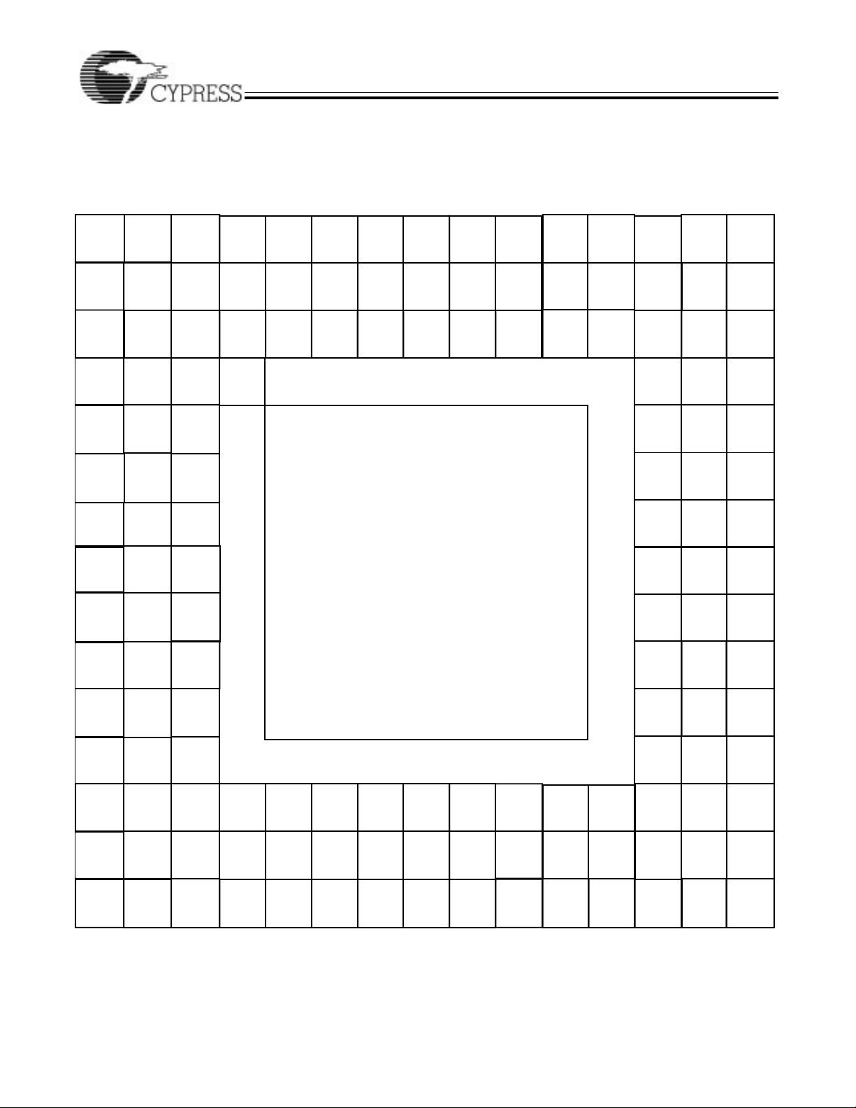
Package Diagrams
VIC068A
144-Pin ThinQuad Flat Pack A144
10
Page 11

Package Diagrams (continued)
VIC068A
145-Pin Plastic Grid Array(Cavity Up)
B144
11
Page 12

Package Diagrams (continued)
145-Pin Grid Array (Cavity Up) G145
VIC068A
12
Page 13

Package Diagrams (continued)
VIC068A
160-Lead Plastic Qu ad Flatpack
N160
13
Page 14

Package Diagrams (continued)
VIC068A
160-Lead C eramic QuadFlatpack
U162
© Cypress Semiconductor Corporation, 1995. The information contained herein is subject to change without notice. Cypress Semiconductor Corporation assumes no responsibility for the use
of any circ uitry other than circui try embodi ed in a Cypress Semi conductor p roduct. Nor does it convey or imply any li cense under patent or other rights . Cypress Semi conductor does not authori ze
its products for use as critical components in life-support systems where a malfunction or failure may reasonably be expected to result in significant injury to the user. The inclusion of Cypress
Semiconductor products in life-support systems application implies that the manufacturer assumes all risk of such use and in doing so indemnifies Cypress Semiconductor against all charges.
 Loading...