

Datasheet VG4616322BQ-7R, VG4616322BQ-7, VG4616322BQ-6, VG4616322BQ-6R, VG4616322BQ-5R Datasheet (VIS)
...Page 1

VG4616321B/VG4616322B
0.3V
±
±
262,144x32x2-Bit
VIS
Overview
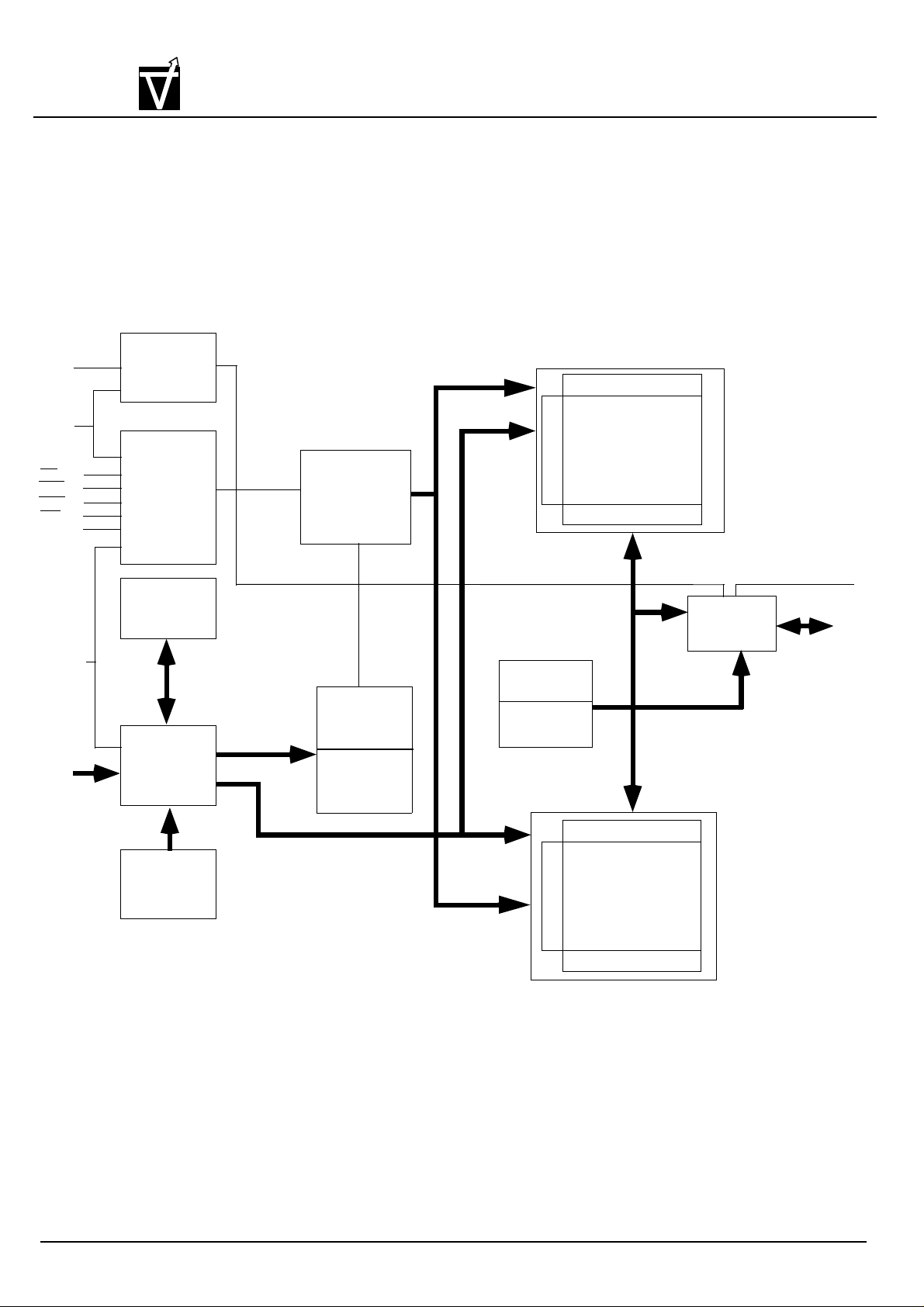
The VG4616321(2) SGRAM is a high-speed CMOS synchronous graphics RAM containing 16M bits. It
is internally configured as a dual 256K x 32 DRAM with a synchronous interface (all signals are registered on
the positive edge of the clock signal, CLK). Each of the 256K x 32 bit banks is organized as 1024 rows by
256 columns by 32 bits. Read and write accesses to the SGRAM are burst oriented; accesses start at a
selected location and continue for a programmed number of locations in a programmed sequence. Accesses
begin with the registration of a BankActivate command which is then followed by a Read or Write command.
The VG4616321(2) provides for programmable Read or Write burst lengths of 1, 2, 4, 8, or full page,
with burst termination option. An Auto Precharge function may be enabled to provide a self-timed row precharge that is initiated at the end of the burst sequence. The refresh functions, either Auto or Self Refresh
are easy to use. In addition, it features the write per bit and the masked block write functions.
By having a programmable Mode register and special mode register, the system can choose the best
suitable modes to maximize its performance. These devices are well suited for applications requiring high
memory bandwidth, and when combined with special graphics functions result in a device particularly well
suited to high performance graphics applications.
Preliminary CMOS Synchronous Graphic RAM
Features
• Fast access time from clock: 4.5/5/5.5ns
• Fast clock rate: 200/166/143 MHz
• Fully synchronous operation
• Internal pipelined architecture
• Dual internal banks(256K x 32-bit x 2-bank)
• Programmable Mode and Special Mode registers
- CAS Latency: 1, 2, or 3
- Burst Length: 1, 2, 4, 8, or full page
- Burst Type: interleaved or linear burst
- Burst Read Single Write
- Load Color or Mask register
• Burst stop function
• Individual byte controlled by DQM0-3
• Block write and write-per-bit capability
• Auto Refresh and Self Refresh
• 2048 refresh cycles/32ms
• Single + 3.3V power supply
• Input Reference Voltage : Vref = 1.5V 0.2V
• Interface: LVTTL and SSTL_3
• JEDEC 100-pin Plastic QFP package
Document:1G5-0145 Rev.1 Page 1
Page 2
VIS
VG4616321B/VG4616322B
262,144x32x2-Bit
Preliminary CMOS Synchronous Graphic RAM
DQ29
DQ30
DQ31
V
V
SSQ
SS
83
84
85
82
81
80
DQ28
V
79
DDQ
78
DQ27
77
DQ26
76
V
SSQ
75
74
DQ24
73
V
DDQ
72
DQ15
71
DQ14
70
V
SSQ
69
DQ13
68
DQ12
67
V
DDQ
66
V
SS
65
V
DD
64
DQ11
63
DQ10
62
V
SSQ
61
DQ9
60
DQ8
59
V
DDQ
58
NC/Vref
57
DQM3
56
DQM1
55
CLK
54
CKE
53
DSF
52
48
47
46
45
NC
50
49
51
A9
A7A6A5A4VSSNC
DQ3
V
DDQ
DQ4
DQ5
V
SSQ
DQ6
DQ7
V
DDQ
DQ16
DQ17
V
SSQ
DQ18
DQ19
V
DDQ
V
DD
V
SS
DQ20
DQ21
V
SSQ
DQ22
DQ23
V
DDQ
DQM0
DQM2
WE
CAS
RAS
CS
BS
A8
1
2
3
4
5
6
7
8
9
10
11
12
13
14
15
16
17
18
19
20
21
22
23
24
25
26
27
28
29
30
V
DQ0
DQ1
DQ2
V
SSQ
100
31
A0
NC
DD
9596979899
3635343332
NC
A3
A2
V
A1
DD
NCNCNCNCNC
91
929394
40
393837
NC
NC
NC
NC
NC
90
88
89
86
87
41
43
42
44
NC
NCNCNCNCNC
NC
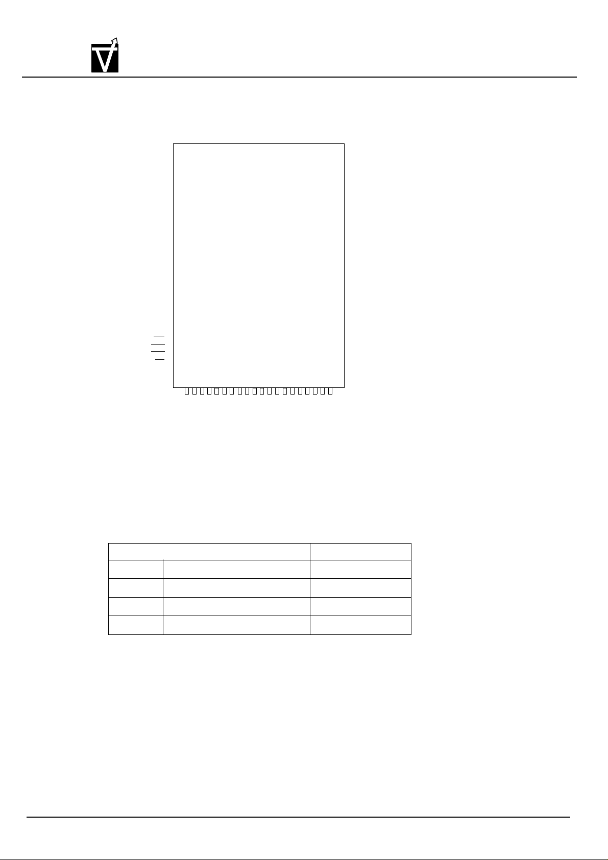
Key Specifications
VG4616321/VG4616322 -5/6/7
t
CK
t
RAS
t
AC
t
RC
Clock Cycle time(min.) 5/6/7 ns
Row Active time(min.) 30/36/40 ns
Access time from CLK(max.) 4.5/5/5.5 ns
Row Cycle time(min.) 45/54/62 ns
Document:1G5-0145 Rev.1 Page 2
Page 3
VIS
Block Diagram
VG4616321B/VG4616322B
262,144x32x2-Bit
Preliminary CMOS Synchronous Graphic RAM
CLK
CKE
CS
RAS
CAS
WE
DSF
A0
A8
BS
~
A9
CLOCK
BUFFER
COMMAND
DECODER
COLUMN
COUNTER
ADDRESS
BUFFER
CONTROL
SIGNAL
GENERATOR
MODE
REGISTER
SPECIAL
MODE
REGISTER
Column Decoder
Row Decoder
COLOR
REGISTER
MASK
REGISTER
Sense Amplifier
1024 X 256 X 32
CELL ARRAY
(BANK #0)
Sense Amplifier
DQs
BUFFER
DQM0~3
DQ0
|
DQ31
REFRESH
COUNTER
Document:1G5-0145 Rev.1 Page 3
1024 X 256 X 32
CELL ARRAY
(BANK #1)
Row Decoder
Column Decoder
Page 4
VG4616321B/VG4616322B
262,144x32x2-Bit
VIS
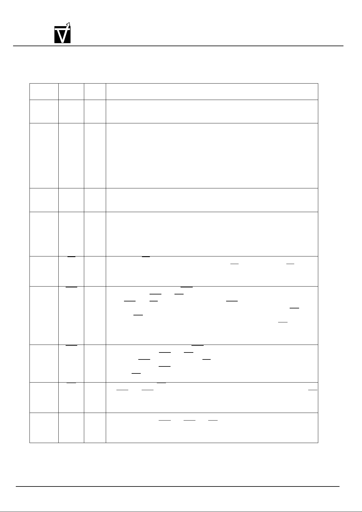
Table 1 shows the details for pin number, symbol, type, and description.
Preliminary CMOS Synchronous Graphic RAM
Table 1. Pin Description of VG4616321
Pin Num-
ber
55 CLK Input Clock: CLK is driven by the system clock. All SGRAM input signals are sampled on
54 CKE Input Clock Enable: CKE activates(HIGH) and deactivates(LOW) the CLK signal. If CKE
29 BS Input Bank Select: BS defines to which bank the BankActivate, Read, Write, or Bank-
30-34,
47-51
28 CS Input Chip Select: CS enables (sampled LOW) and disables (sampled HIGH) the com-
27 RAS Input Row Address Strobe: The RAS signal defines the operation commands in con-
26 CAS Input Column Address Strobe: The CAS signal defines the operation commands in
25 WE Input Write Enable: The WE signal defines the operation commands in conjunction with
53 DSF Input Define Special Function: The DSF signal defines the operation commands in
Symbol Type Description
the positive edge of CLK. CLK also increments the internal burst counter and control the output registers.
goes low synchronously with clock (set-up and hold time same as other inputs), the
internal clock is suspended from the next clock cycle and the state of output and
burst address is frozen as long as the CKE remains low. When both banks are in
the idle state, deactivating the clock controls the entry to the Power Down and Self
Refresh modes. CKE is synchronous except after the device enters Power Down
and Self Refresh modes, where CKE becomes asynchronous until after exiting the
same mode. The input buffers, including CLK, are disabled during Power Down
and Self Refresh modes providing low standby power.
Precharge command is being applied. BS is also used to program the 10th bit of
the Mode and Special Mode registers.
A0-A9 Input Address Inputs: A0-A9 are sampled during the BankActivate command (row
address A0-A9) and Read/Write command (column address A0-A7 with A9 defining Auto Precharge) to select one location out of the 256K available in the respective bank. During a Precharge command, A9 is sampled to determine if both banks
are to be precharged (A9 = HIGH). The address inputs also provide the op-code
during a Mode Register Set or Special Mode Register Set command.
mand decoder. All commands are masked when CS is sampled HIGH. CS provides
for external bank selection on systems with multiple banks. It is considered part of
the command code.
junction with the CAS and WE signals, and is latched at the positive edges of CLK.
When RAS and CS are asserted “LOW” and CAS is asserted “HIGH”, either the
BankActivate command or the Precharge command is selected by the WE signal.
When the WE is asserted “HIGH” the BankActivate command is selected and the
bank designated by BS is turned on to the active state. When the WE is asserted
"LOW", the Precharge command is selected and the bank designated by BS is
switched to the idle state after precharge operation.
conjunction with the RAS and WE signals, and it is latched at the positive edges of
CLK. When RAS is held “HIGH” and CS is asserted “LOW”, the column access is
started by asserting CAS “LOW”. Then, the Read or Write command is selected by
asserting WE “LOW” or “HIGH”.
the RAS and CAS signals, and it is latched at the positive edges of CLK. The WE
input is used to select the BankActivate or Precharge command and Read or Write
command.
conjunction with the RAS and CAS and WE signals, and it is latched at the positive
edges of CLK. The DSF input is used to select the masked write disable/enable
command and block write command, and the Special Mode Register Set cycle.
Document:1G5-0145 Rev.1 Page 4
Page 5

VIS
0.3V
±
VG4616321B/VG4616322B
262,144x32x2-Bit
Preliminary CMOS Synchronous Graphic RAM
23,56,24,57DQM0-
DQM3
97,98,100,
1,3,4,6,7,
60,61,63,
64,68,69,
71,72,9,
10,12,13,
17,18,20,
21,74,75,
77, 78,80,
81, 83, 84
30,36-45,
52,86-95
58 NC/Vref -/Input No connect/Input Voltage Reference : It must be unconnected when the LVTTL
2,8,14,22,
59,67,73,
79
5,11,19,
62,70,76,
82,99
15,35,65,96V
DQ0-
DQ31
NC - No Connect: These pins should be left unconnected.
V
DDQ
V
SSQ
DD
Input Data Input/Output Mask: DQM0-DQM3 are byte specific, nonpersistent I/O buffer
controls. The I/O buffers are placed in a high-z state when DQM is sampled HIGH.
Input data is masked when DQM is sampled HIGH during a write cycle. Output data
is masked (two-clock latency) when DQM is sampled HIGH during a read cycle.
DQM3 masks DQ31-DQ24, DQM2 masks DQ23-DQ16, DQM1 masks DQ15-DQ8,
and DQM0 masks DQ7-DQ0.
Input/
Output
Supply DQ Power: Provide isolated power to DQs for improved noise immunity.
Supply DQ Ground: Provide isolated ground to DQs for improved noise immunity.
Supply
Data I/O: The DQ0-31 input and output data are synchronized with the positive
edges of CLK. The I/Os are byte-maskable during Reads and Writes. The DQs also
serve as column/byte mask inputs during Block Writes.
interface is used in the SGRAM. It must be applied to Vref (1.5V) when the SSTL-3
interface is used in the SGRAM.
Power Supply: +3.3V
16,46,66,85V
Supply Ground
SS
Document:1G5-0145 Rev.1 Page 5
Page 6
VG4616321B/VG4616322B
262,144x32x2-Bit
VIS
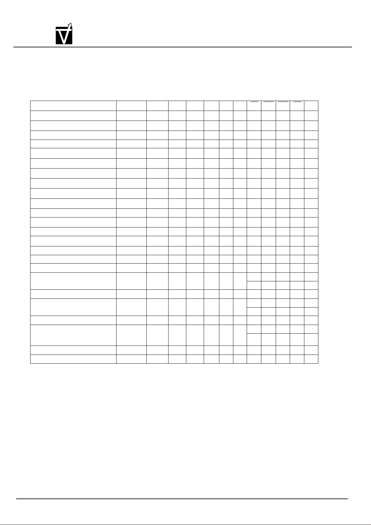
Operation Mode
Fully synchronous operations are performed to latch the commands at the positive edges of CLK. Table 2
shows the truth table for the operation commands.
BankActivate & Masked Write Disable
BankActivate & Masked Write Enable
BankPrecharge Any H X X V L X L L H L L
PrechargeAll Any H X X X H X L L H L L
Write
Block Write Command
Write and AutoPrecharge
Block Write and AutoPrecharge
Read
Read and AutoPrecharge
Mode Register Set Idle H X X V L V L L L L L
Special Mode Register Set
No-Operation Any H X X X X X L H H H X
Burst Stop
Device Deselect Any H X X X X X H X X X X
AutoRefresh Idle H H X X X X L L L H L
SelfRefresh Entry Idle H L X X X X L L L H L
SelfRefresh Exit Idle
Clock Suspend Mode Entry Active H L X X X X X X X X X
Power Down Mode Entry
Clock Suspend Mode Exit Active L H X X X X X X X X X
Power Down Mode Exit Any
Data Write/Output Enable Active H X L X X X X X X X X
Data Write/Output Disable Active H X H X X X X X X X X
Note: 1. V = Valid X = Don’t Care L = Low level H = High level
2. CKEn signal is input level when commands are provided.
CKEn-1 signal is input level one clock cycle before the commands are provided.
3. These are states of bank designated by BS signal.
4. Device state is 1, 2, 4, 8, and full page burst operation.
5. The Special Mode Register Set is also available in Row Active State.
6. Power Down Mode can not entry in the burst operation.
When this command assert in the burst cycle, device state is clock suspend mode.
7. DQM0-3
Preliminary CMOS Synchronous Graphic RAM
Table 2. Truth Table (Note(1), (2))
Command State CKEn-1 CKEn
(3)
Idle
(3)
Idle
(3)
Active
(3)
Active
(3)
Active
(3)
Active
(3)
Active
(3)
Active
(5)
Idle
(4)
Active
(SelfRefresh)
(6)
Any
(Power-
Down)
H X X V V V L L H H L
H X X V V V L L H H H
H X X V L V L H L L L
H X X V L V L H L L H
H X X V H V L H L L L
H X X V H V L H L L H
H X X V L V L H L H L
H X X V H V L H L H L
H X X X X V L L L L H
H X X X X X L H H L L
L H X X X X H X X X X
H L X X X X H X X X X
L H X X X X H X X X X
DQM
(7)
BS A9 A0-8 CS RAS CAS WE DSF
L H H H X
L H H H L
L H H H L
Document:1G5-0145 Rev.1 Page 6
Page 7

VG4616321B/VG4616322B
262,144x32x2-Bit
VIS
Commands
1 BankActivate & Masked Write Disable command
(RAS = ”L”, CAS = ”H”, WE = ”H”, DSF = ”L”, BS = Bank, A0-A9 = Row Address)
The BankActivate command activates the idle bank designated by the BS (Bank Select) signal. By
latching the row address on A0 to A9 at the time of this command, the selected row access is initiated.
The read or write operation in the same bank can occur after a time delay of t
bank activation. A subsequent BankActivate command to a different row in the same bank can only be
issued after the previous active row has been precharged (refer to the following figure). The minimum
time interval between successive BankActivate commands to the same bank is defined by tRC(min.).
The SGRAM has two internal banks on the same chip and shares part of the internal circuitry to reduce
chip area, therefore it restricts the back-to-back activation of both banks. t
mum time required between activating different banks. After this command is used, the Write command
and the Block Write command perform the no mask write operation.
CLK
Preliminary CMOS Synchronous Graphic RAM
T0 T1 T2 T3 Tn+3 Tn+4 Tn+5 Tn+6
(min.) from the time of
RCD
(min.) specifies the mini-
RRD
ADDRESS
COMMAND
: “H” or “L”
Bank A
Row Addr.
Bank A
Activate
RAS-CAS delay (t
NOP
RCD
)
NOP
Bank A
Col Addr.
R/W A with
AutoPrecharge
RAS Cycle time (tRC)
Bank A
Row Addr.
Bank B
Activate
AutoPrecharge
Begin
RAS-RAS delay time (t
NOP
RRD
)
NOP
BankActivate Command Cycle (Burst Length = n, CAS Latency = 3)
2 BankActivate & Masked Write Enable command (refer to the above figure)
(RAS = ”L”, CAS = ”H”, WE = ”H”, DSF = ”H”, BS = Bank, A0-A9 = Row Address)
The BankActivate command activates the idle bank designated by BS signal. After this command is
performed, the Write command and the Block Write command perform the masked write operation. In
the masked write and the masked block write functions, the I/O mask data that was stored in the write
mask register is used.
3 BankPrecharge command
(RAS = ”L”, CAS = ”H”, WE = ”L”, DSF = ”L”, BS = Bank, A9 = ”L”, A0-A8 = Don’t care)
The BankPrecharge command precharges the bank designated by BS signal. The precharged
bank is switched from the active state to the idle state. This command can be asserted anytime after
t
(min.) is satisfied from the BankActivate command in the desired bank. The maximum time any
RAS
bank can be active is specified by t
any active bank within t
(max.). At the end of precharge, the precharged bank is still the idle state and
RAS
(max.). Therefore, the precharge function must be performed in
RAS
ready to be activated again.
Bank A
Row Addr.
Bank A
Activate
4 PrechargeAll command
(RAS = ”L”, CAS = ”H”, WE = ”L”, DSF = ”L”, BS = Don’t care, A9 = ”H”, A0-A8 = Don’t care)
The PrechargeAll command precharges both banks simultaneously. Even if both banks are not in
the active state, the PrechargeAll command can be issued. Both banks are then switched to the idle
state.
5 Read command
(RAS = ”H”, CAS = ”L”, WE = ”H”, DSF = ”L”, BS = Bank, A9 = ”L”, A0-A7 = Column Address, A8 = Don’t care)
Document:1G5-0145 Rev.1 Page 7
Page 8
VIS
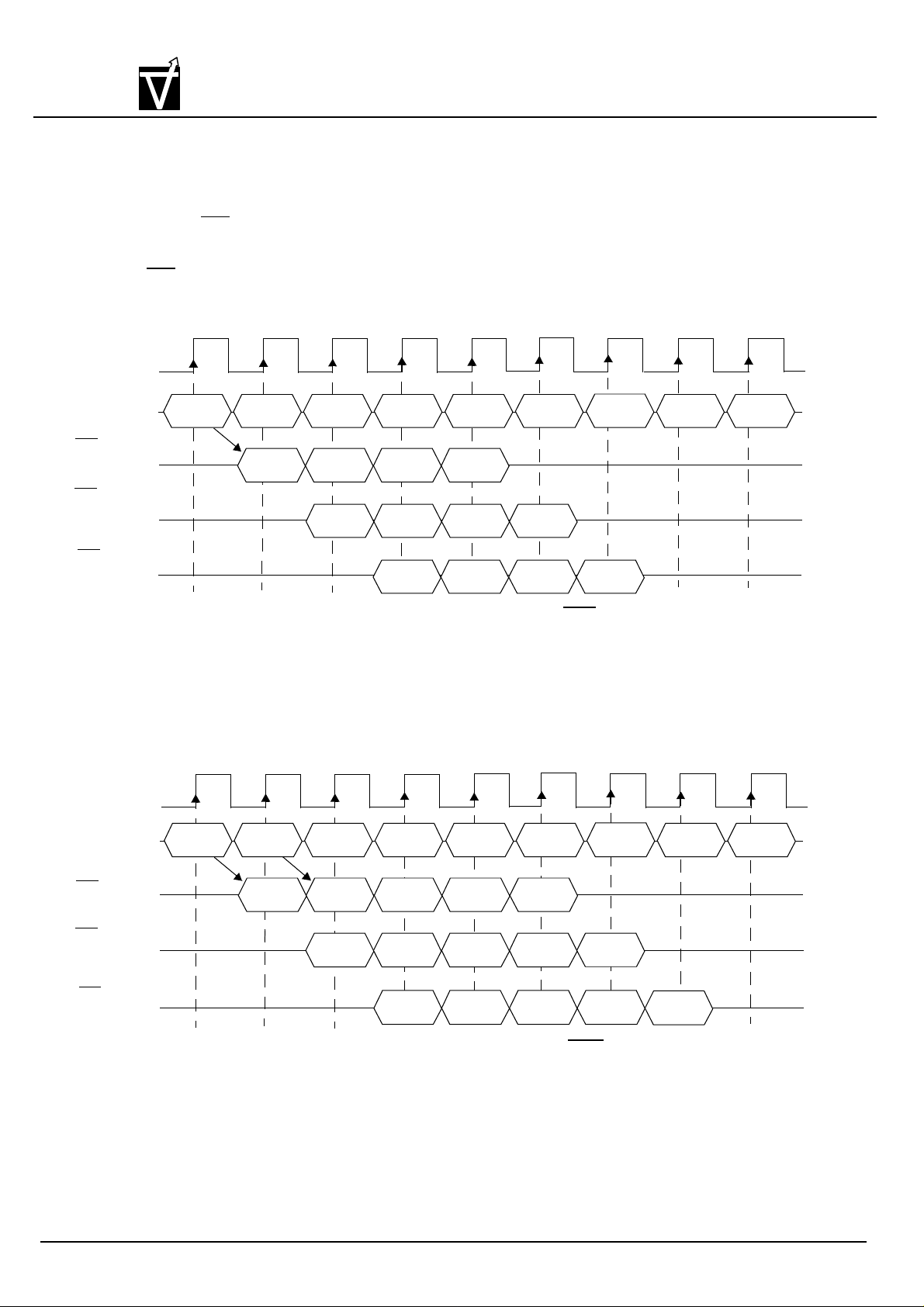
in an active bank. The bank must be active for at least t
During read bursts, the valid data-out element from the starting column address will be available
following the CAS latency after the issue of Read command. Each subsequent data-out element will
be valid by the next positive clock edge (refer to the following figure). The DQs goes into high-impedance at the end of the burst, unless other command was initiated. The burst length, burst sequence,
and CAS latency are determined by the mode register which is already prgrammed.A full-page burst
will continue until terminated (at the end of the page it will wrap to column 0 and continue).
VG4616321B/VG4616322B
262,144x32x2-Bit
Preliminary CMOS Synchronous Graphic RAM
The Read command is used to read burst of data on consecutive clock cycles from an active row
(min.) before Read command is issued.
RCD
T6
NOP
3
DOUT A
2
3
CLK
COMMAND
CAS Iatency = 1
t
,DQ’s
CK1
CAS Iatency = 2
t
,DQ’s
CK2
CAS Iatency = 3
t
,DQ’s
CK3
T0
READ A
T1
NOP
DOUT A
T2
NOP
DOUT A
0
DOUT A
T3
NOP
DOUT A
1
DOUT A
0
DOUT A
T4
NOP
DOUT A
2
DOUT A
1
DOUT A
0
T5
NOP
3
DOUT A
2
DOUT A
1
Burst Read Operation (Burst Length = 4, CAS Latency = 1, 2, 3)
The read data appears on the DQs subjects to the values on the DQM inputs two clocks early (i.e.
DQM latency is two clocks for output buffers). A read burst without auto precharge function may be
interrupted by a subsequent Read or Write/Block Write command to the same bank or the other
active bank before the end of burst length. It may be interrupted by a BankPrecharge/PrechargeAll
command to the same bank too. The interrupt comes from Read command can occur on any clock
cycle following a previous Read command (refer to the following figure).
T0
T1
T2
T3
T4
T5
T6
T7 T8
NOP
T7 T8
NOP
CLK
COMMAND
CAS Iatency = 1
t
,DQ’s
CK1
CAS Iatency = 2
t
,DQ’s
CK2
CAS Iatency = 3
t
,DQ’s
CK3
READ A
READ B
DOUT A
NOP
DOUT B
0
DOUT A
NOP
DOUT B
0
DOUT B
0
DOUT A
NOP
DOUT B
1
DOUT B
0
DOUT B
0
NOP
DOUT B
2
DOUT B
1
DOUT B
0
NOP
3
DOUT B
DOUT B
3
2
2
1
Read Interrupted by a Read (Burst Length = 4, CAS Latency = 1, 2, 3)
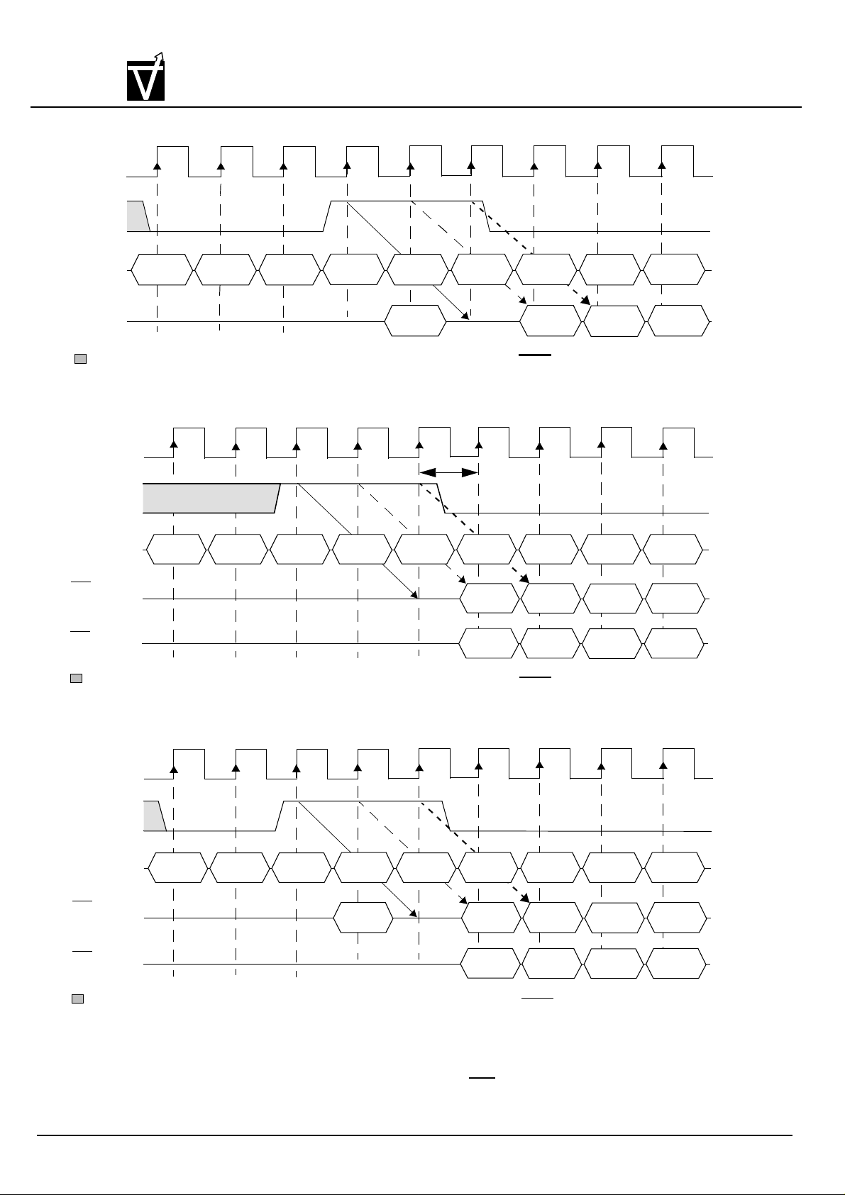
The DQM inputs are used to avoid I/O contention on DQ pins when the interrupt comes from
Write/Block Write command. The DQMs must be asserted (High) at least two clocks prior to the
Write/Block Write command to suppress data-out on DQ pins. To guarantee DQ pins against the I/O
contention, a single cycle with high-impedance on DQ pins must occur between the last read data
and the Write/Block Write command (refer to the following three figures). If the data output of burst
read occurs at the second clock of burst write, the DQMs must be asserted (High) at least one clock
prior to the Write/Block Write command to avoid internal bus contention.
NOP
DOUT B
NOP
3
Document:1G5-0145 Rev.1 Page 8
Page 9
VIS
VG4616321B/VG4616322B
262,144x32x2-Bit
Preliminary CMOS Synchronous Graphic RAM
CLK
DQM
COMMAND
DQ’s
: “H” or “L”
CLK
DQM
COMMAND
T0
NOP
T0
NOP
T1
READ A
T2
NOP
T3
NOP
T4
NOP
DOUT A
0
Must be Hi-Z before
the Write Command
Read to Write interval (Burst Length
T1
NOP
T2
BANK A
ACTIVATE
T3
NOP
T4
1 Clk Interval
READ A
T5
NOP
°Ÿ
T5
WRITE A
T6
WRITE B
DINB
0
4, CAS Latency = 3)
T6
NOP
T7 T8
NOP
DINB
1
T7
NOP NOP
DINB
T8
NOP
2
CAS Iatency = 1
t
,DQ’s
CK1
CAS Iatency = 2
t
,DQ’s
CK2
: “H” or “L”
CLK
DQM
COMMAND
CAS Iatency = 1
t
,DQ’s
CK1
CAS Iatency = 2
t
,DQ’s
CK2
: “H” or “L”
T0
NOP
Must be Hi-Z before
the Write Command
Read to Write interval (Burst Length
T1
NOP
T2
READ A
T3
NOP
DOUT A
T4
NOP
0
Must be Hi-Z before
the Write Command
Read to Write interval (Burst Length
DIN A
DIN A
°Ÿ
T5
WRITE B
DIN B
DIN B
°Ÿ
0
0
0
DIN A
1
DIN A
1
4, CAS Latency = 1, 2)
T6
NOP
DIN B
DIN B
1
1
0
4, CAS Latency = 1, 2)
DIN A
DIN A
T7
DINB
DIN B
NOP
DIN A
2
2
2
2
DIN A
T8
NOP
DIN B
DIN B
3
3
3
3
A read burst without auto precharge function may be interrupted by a BankPrecharge/
PrechargeAll command to the same bank. The following figure shows the optimum time that
BankPrecharge/PrechargeAll command is issued in different CAS latency.
Document:1G5-0145 Rev.1 Page 9
Page 10
VIS
VG4616321B/VG4616322B
262,144x32x2-Bit
Preliminary CMOS Synchronous Graphic RAM
T6
t
RP
NOP
3
DOUT A
2
T7
Bank
Row
Activate
3
T8
NOP
CLK
ADDRESS
COMMAND
CAS Iatency = 1
t
,DQ’s
CK1
CAS Iatency = 2
t
,DQ’s
CK2
CAS Iatency = 3
t
,DQ’s
CK3
T0
Bank
Col A
READ A
T1
NOP
DOUT A
T2
NOP
DOUT A
0
DOUT A
T3
NOP
DOUT A
1
DOUT A
0
DOUT A
T4
Bank(s)
Precharge
DOUT A
2
DOUT A
1
DOUT A1DOUT A
0
T5
NOP
3
DOUT A
2
Read to Precharge (CAS Latency = 1, 2, 3)
6 Read and AutoPrecharge command
(RAS = ”H”, CAS = ”L”, WE = ”H”, DSF = ”L”, BS = Bank, A9 = ”H”, A0-A7 = Column Address, A8 = Don’t care)
The Read and AutoPrecharge command automatically performs the precharge operation after the read
operation. Once this command is given, any subsequent command can not occur within a time delay of
{tRP(min.) + burst length}. At full-page burst, only read operation is performed in this command and the auto pre-
charge function is ignored.
7 Write command
(RAS = ”H”, CAS = ”L”, WE = ”L”, DSF = “L”, BS = Bank, A9 = ”L”, A0-A7 = Column Address, A8 = Don’t care)
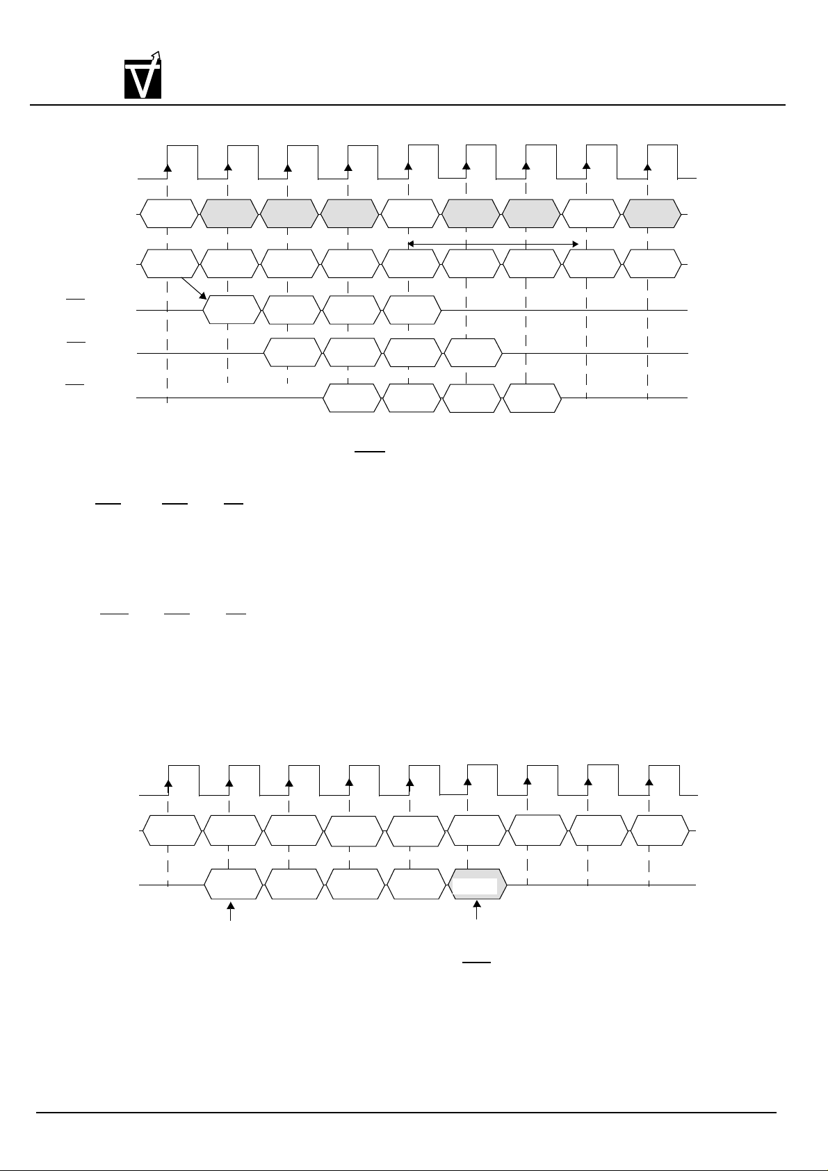
The Write command is used to write burst of data on consecutive clock cycles from an active row in an
active bank. The bank must be active for at least t
(min.) before Write command is issued. During write
RCD
bursts, the first valid data-in element will be registered coincident with the Write command. Subsequent data elements will be registered on each successive positive clock edge (refer to the following figure). The DQs remains
high-impedance at the end of the burst, unless other command was initiated. The burst length and burst
sequence are determined by the mode register which is already programmed. A full-page burst will continue
until terminated (at the end of the page it will wrap to column 0 and continue).
T6
NOP
T7
NOP
T8
NOP
CLK
COMMAND
DQ0 - DQ3
T0
NOP
The first data element and the write
are registered on the same clock edge.
T1
WRITE A
DIN A
T2
NOP
DIN A
0
T3
NOP
DIN A
1
T4
NOP
DIN A
2
T5
NOP
don’t care
3
Extra data is masked.
Burst Write Operation (Burst Length = 4, CAS Latency = 1, 2, 3)
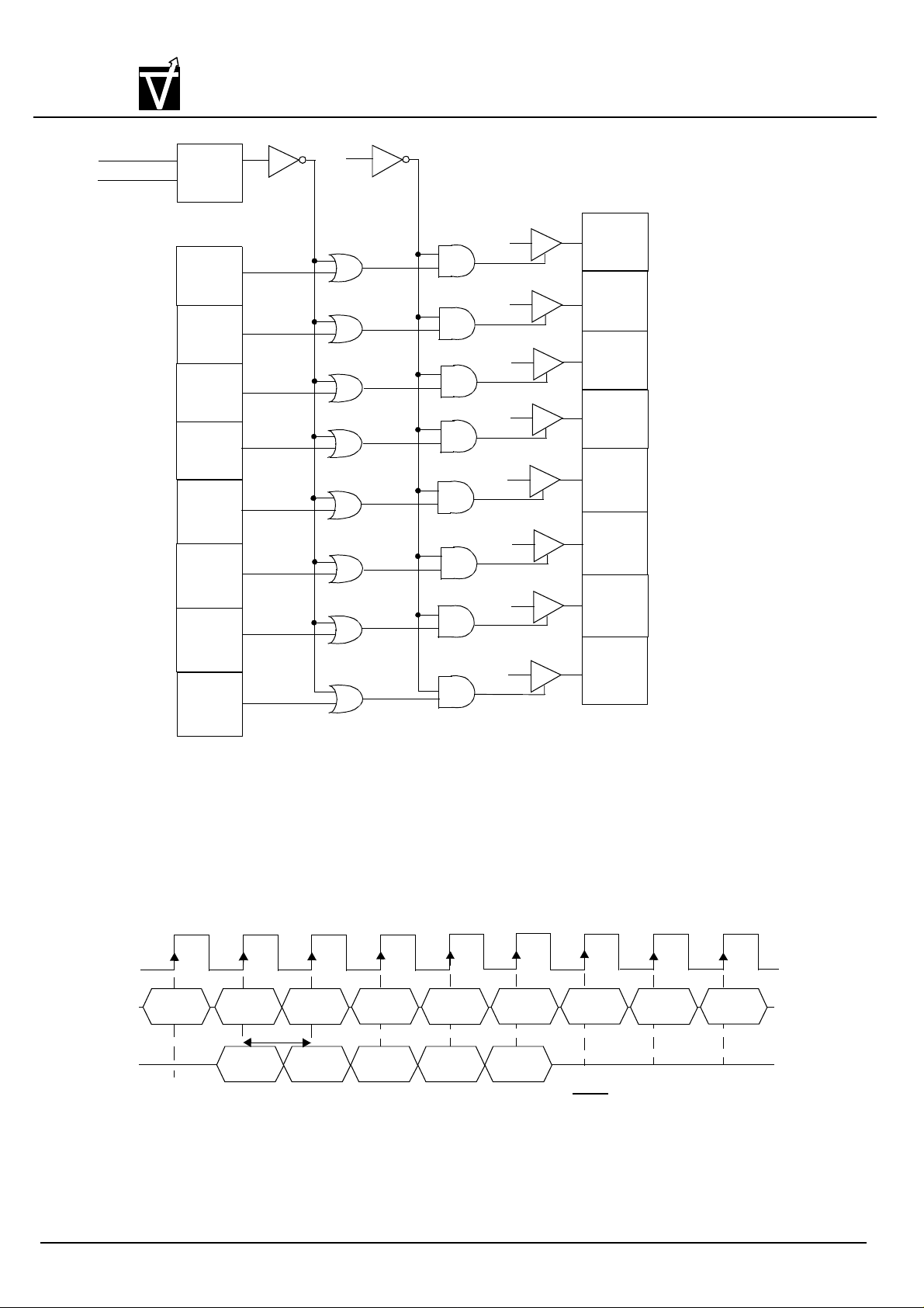
Any Write performed to a row that was opened via an BankAcitvate & Masked Write Enable command is a
masked write (Write-Per-Bit). Data is written to the 32 cells (bits) at the selected column location subject to the
data stored in the Mask register. The overall mask consists of the DQM inputs, which mask on a per-byte
basis, and the Mask register, which masks on a per-bit basis. This is shown in the following block diagram.
Document:1G5-0145 Rev.1 Page 10
Page 11
VIS
VG4616321B/VG4616322B
262,144x32x2-Bit
Preliminary CMOS Synchronous Graphic RAM
DSF
BankActivate
command
D
CK
MR7
MR6
MR5
MR4
MR3
MR2
Q
DQM0
DRAM
CELL
DQ7
DQ6
DQ5
DQ4
DQ3
DQ2
DQ1
MR1
DQ0
MR0
0 = Masked
1 = Not Masked
Note: Only lower byte is shown. The operation is identical for other bytes.
Write Per Bit (I/O Mask) Block Diagram
A write burst without auto precharge function may be interrupted by a subsequent Write/Block
Write, BankPrecharge/PrechargeAll, or Read command before the end of burst length. The interrupt
comes from Write/Block Write command can occur on any clock cycle following the previous Write
command ( refer to the following figure).
T6
NOP
T7 T8
NOP
CLK
COMMAND
T0
NOP WRITE A
T1
1 Clk Interval
T2
WRITE B
T3
NOP
T4
NOP
T5
NOP
NOP
DQ’s
DIN A
DIN B
0
DIN B
0
DIN B
1
DIN B
2
3
Write Interrupted by a Write (Burst Length = 4, CAS Latency = 1, 2, 3)
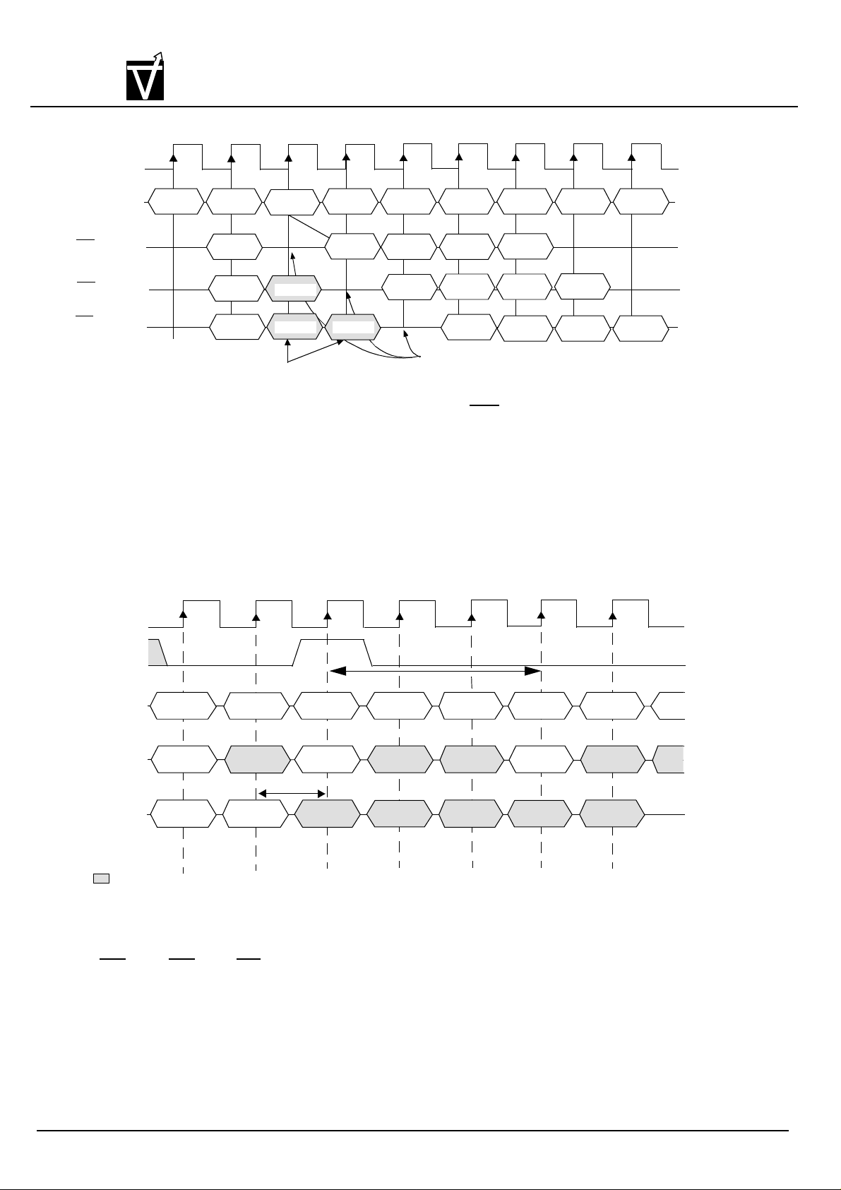
The Read command that interrupts a write burst without auto precharge function should
be issued one cycle after the clock edge at which the last data-in element is registered. In
order to avoid data contention, input data must be removed from the DQs at least one clock
cycle before the first read data appears on the outputs (refer to the following figure). Once the
Read command is registered, the data inputs will be ignored, and writes will not be executed.
Document:1G5-0145 Rev.1 Page 11
Page 12
VIS
VG4616321B/VG4616322B
262,144x32x2-Bit
Preliminary CMOS Synchronous Graphic RAM
T6
NOP
DOUT B
2
DOUT B
1
0
DOUT B
T7 T8
3
DOUT B
2
DOUT B
1
NOP
CLK
COMMAND
CAS latency = 1
t
,DQ’s
CK1
CAS latency = 2
t
,DQ’s
CK2
CAS latency = 3
t
,DQ’s
CK3
T0
NOP
T1
WRITE A
DIN A
DIN A
DIN A
Input data for the write is masked
T2
READ B NOP
0
0
don’t care
don’t care
0
T3
NOP
DOUT B
don’t care
T4
DOUT B
0
DOUT B
T5
NOP
DOUT B
1
DOUT B
0
DOUT B
Input data must be removed from DQ’
cycle before the Read data appears on the outputs to avoid
data contention
Write Interrupted by a Read (Burst Length = 4, CAS Latency = 1, 2, 3)
The BankPrecharge/PrechargeAll command that interrupts a write burst without auto precharge function should be issued m cycles after the clock edge at which the last data-in element
is registered, where m equals tWR/tCK rounded up to the next whole number. In addition, the
DQM signals must be used to mask input data, starting with the clock edge following the last
data-in element and ending with the clock edge on which the BankPrecharge/PrechargeAll command is entered (refer to the following figure).
NOP
3
DOUT B
2
s at least one clock
3
T0 T1 T2 T3 T4 T5 T6
CLK
DQM
t
RP
COMMAND
ADDRESS
DQ
:don’t care
WRITE NOP
BANK
COLn
DIN
n
NOP
DIN
n+1
t
WR
Precharge
BANK (S)
Write to Precharge
NOP
Activate
ROW
NOP
When Burst-Read and Single-Write mode is selected , the write burst length is 1 regardless of the
read burst length (refer to Figures 21 and 22 in Timing Waveforms).
8 Block Write command
(RAS = “H” , CAS = “L” , WE = “L”, DSF = “H” , BS =Bank , A9 = “L” , A3-A7 = Column Address, DQ0-DQ31
= Column Mask)
The block writes are non-burst accesses that write to eight column locations simultaneously. A single
data value, which was previously loaded in the Color register, is written to the block of eight consecutive column locations addressed by inputs A3-A7. The information on the DQs which is registered coincident with
the Block Write command is used to mask specific column/byte combinations within the block . The mapping
of the DQ inputs to the column/byte combinations is shown in following table.
Document:1G5-0145 Rev.1 Page 12
Page 13

VIS
DQ
inputs
DQ0 0 0 0 0~7 DQ16 0 0 0 16~23
DQ1 0 0 1 0~7 DQ17 0 0 1 16~23
DQ2 0 1 0 0~7 DQ18 0 1 0 16~23
DQ3 0 1 1 0~7 DQ19 0 1 1 16~23
DQ4 1 0 0 0~7 DQ20 1 0 0 16~23
DQ5 1 0 1 0~7 DQ21 1 0 1 16~23
DQ6 1 1 0 0~7 DQ22 1 1 0 16~23
DQ7 1 1 1 0~7 DQ23 1 1 1 16~23
DQ8 0 0 0 8~15 DQ24 0 0 0 24~31
DQ9 0 0 1 8~15 DQ25 0 0 1 24~31
DQ10 0 1 0 8~15 DQ26 0 1 0 24~31
DQ11 0 1 1 8~15 DQ27 0 1 1 24~31
DQ12 1 0 0 8~15 DQ28 1 0 0 24~31
DQ13 1 0 1 8~15 DQ29 1 0 1 24~31
DQ14 1 1 0 8~15 DQ30 1 1 0 24~31
DQ15 1 1 1 8~15 DQ31 1 1 1 24~31
VG4616321B/VG4616322B
262,144x32x2-Bit
Preliminary CMOS Synchronous Graphic RAM
Column Address DQ Planes
A2 A1 A0 A2 A1 A0
Controlled
DQ
Inputs
Column Address DQ Planes
Controlled
The overall Block Write mask consists of a combination of the DQM inputs, the Mask register,
and the column/byte mask information, as shown in the following diagram. The DQM and Mask register masking operates as for normal Write command, with the exception that the mask information
is applied simultaneously to all eight columns. Therefore, in a Block Write, a given bit is written only if
a ”0” was registered for the corresponding DQM input, a ”1” was registered for the corresponding DQ
signal, and the corresponding bit in the Mask register is ”1”.
A block write access requires a time period of t
m NOP cycles, m equals (t
command. However, BankActivate or BankPrecharge commands to the other bank are allowed.
When following a Block Write with a BankPrecharge or PrechargeAll command to the same bank, t
must be met.
BWC-tCK
) /tCK rounded up to the next whole number, after the Block Write
to execute, so in general, there should be
BWC
BPL
Document:1G5-0145 Rev.1 Page 13
Page 14

VIS
VG4616321B/VG4616322B
262,144x32x2-Bit
Preliminary CMOS Synchronous Graphic RAM
Block of Columns
(selected by A3-A7 registered
coincident with Block Write command)
Row in Bank
(selected by A0-A9,
and BS registered
coincident with BankActivate
Command)
Column Mask
on the DQ
inputs
(registered
coincident
with Block
Write Command
BankActivate
command
Mask Register
(previously loaded
from corresponding
DQ inputs
Note: Only lower byte is shown. The operation is identical for other bytes.
DSF
D Q
CK
MR0
MR1
MR2
MR3
MR4
MR5
MR6
MR7
DQ0
DQ1
DQ2
DQ3
DQ4
DQ5
DQ6
DQ7
DQMO
CR0
CR1
CR2
CR3
CR4
CR5
CR6
CR7
Block-Write Masking Block Diagram
Document:1G5-0145 Rev.1 Page 14
Page 15
VIS
9 Write and AutoPrecharge command (refer to the following figure)
CLK
VG4616321B/VG4616322B
262,144x32x2-Bit
Preliminary CMOS Synchronous Graphic RAM
(RAS = “H” , CAS = “L” , WE = “L” , DSF=”L” , BS = Bank, A9 = ”H”, A0-A7 = Column Address, A8 =
Don’t care)
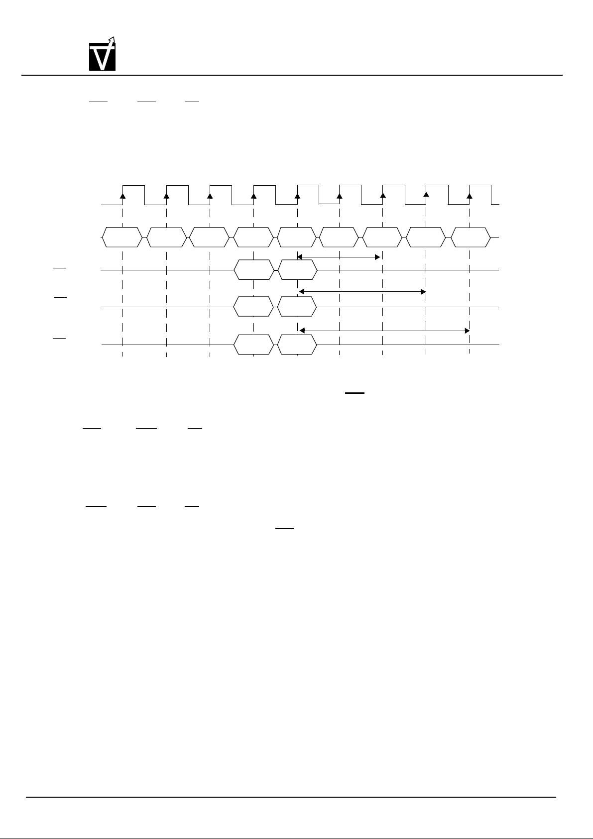
The Write and AutoPrecharge command performs the precharge operation automatically after
the write operation. Once this command is given, any subsequent command can not occur within a
time delay of {burst length + tWR + tRP(min.)}. At full-page burst, only write operation is performed in
this command and the auto precharge function is ignored.
T0
T1
T2
T3
T4
T5
T6
T7
T8
COMMAND
CAS latency = 1
t
,DQ’s
ck1
CAS latency = 2
t
,DQ’s
ck2
CAS latency = 3
t
,DQ’s
ck3
Bank A
Activate
t
DAL
NOP
= t
+ t
WR
RP
NOP
Write A
Auto Precharge
DIN A
DIN A
DIN A
NOP
DIN A
0
DIN A
0
DIN A
0
NOP
t
DAL
1
*
*
1
1
*
Begin AutoPrecharge
*
Bank can be reactivated at completion of t
NOP
t
DAL
NOP
t
DAL
Burst Write with Auto-Precharge (Burst Length = 2, CAS Latency = 1, 2, 3)
10 Block Write and AutoPrecharge command
(RAS = “H” , CAS = “L” , WE = “H”, DSF = “H” , BS = Bank , A9 = “H” , A3-A7 = Column Address, A8
= Don’t care DQ0-DQ31 = Column Mask)
The Block Write and AutoPrecharge command performs the precharge operation automatically after
the block write operation. Once this command is given, any subsequent command can not occur within a
time delay of {t
11 Mode Register Set command
(RAS = “L” , CAS = ”L”, WE = “L” , DSF = “L” , BS , A0-A9 = Register Data)
The mode register stores the data for controlling the various operating modes of SGRAM. The Mode
Register Set command programs the values of CAS latency. Addressing Mode and Burst Length in the
Mode register to make SGRAM useful for variety of different applications. The default values of the Mode
Register after power-up are undefined, therefore this command must be issued at the power-up
sequence. The state of pins A0-A9 and BS in the same cycle is the data written in the mode register. One
clock cycle is required to complete the write in the mode register (refer to the following figure ). The mode
register contents can be changed using the same command and the clock cycle requirements during
operation as long as both banks are in the idle state.
+ tRP (min.)}.
BPL
NOP
DAL
Document:1G5-0145 Rev.1 Page 15
Page 16

VIS
VG4616321B/VG4616322B
262,144x32x2-Bit
Preliminary CMOS Synchronous Graphic RAM
CLK
CKE
RAS
CAS
WE
DSF
T7
T8
T10T9
tCK2
T1
T2 T3 T4
Clock min
T0
CS
BS
T5 T6
A9
Address key
A0-A8
DQM
t
DQ
Hi-Z
PrechargeAll
Mode Register Set Cycle (
RP
Mode Register
Set Command
Any
Command
CAS
Latency = 1, 2, 3)
The mode register is divided into various fields depending on functionality.
• Burst Length Field (A2~A0)
This field specifies the data length of column access using the A2~A0 pins and selects the
Burst Length to be 1, 2, 4, 8, or full page.
A2 A1 A0 Burst Length
0 0 0 1
0 0 1 2
0 1 0 4
0 1 1 8
1 0 0 Reserved
1 0 1 Reserved
1 1 0 Reserved
1 1 1 Full Page
Document:1G5-0145 Rev.1 Page 16
Page 17
VG4616321B/VG4616322B
≤
262,144x32x2-Bit
VIS
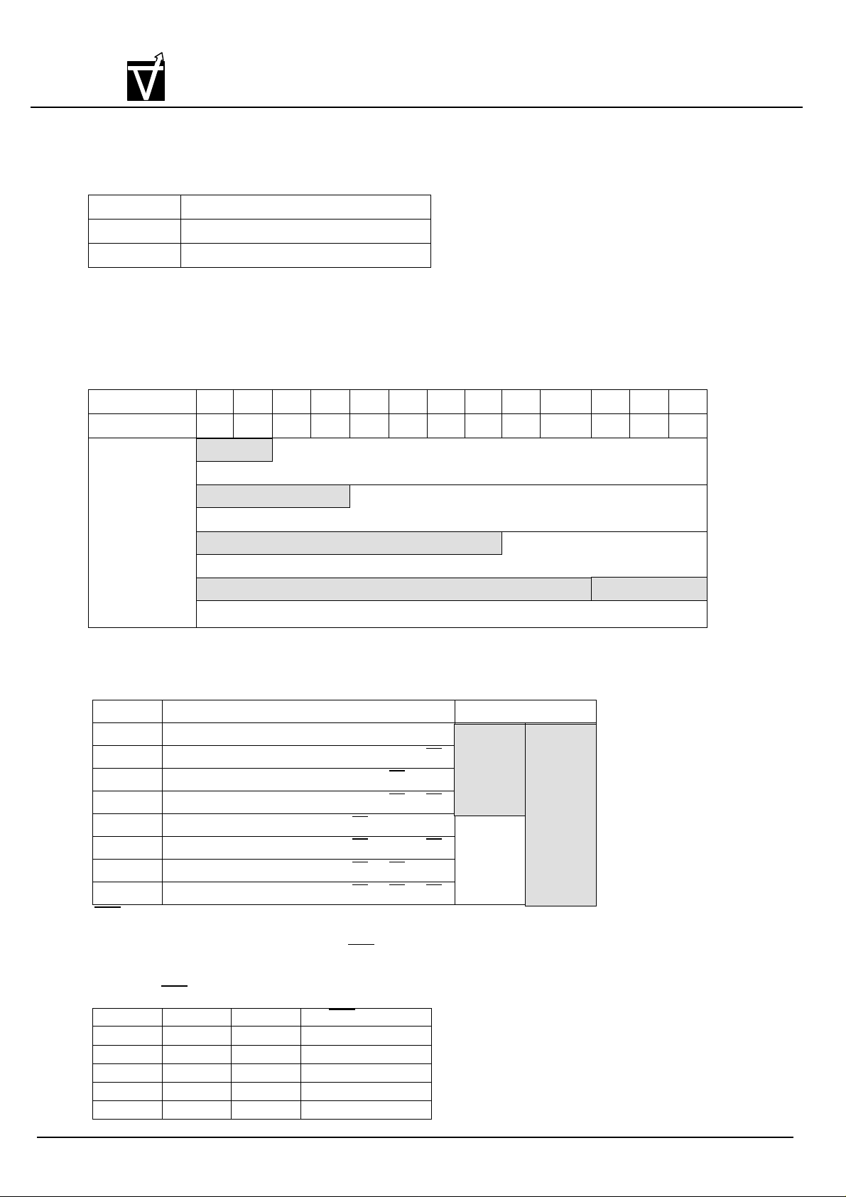
• Addressing Mode Select Field (A3)
The Addressing Mode can be one of two modes, Interleave Mode or Sequential Mode.
Sequential Mode supports burst length of 1, 2, 4, 8, or full page. But, lnterleave Mode only supports
burst length of 4 and 8.
A3 Addressing Mode
--- Addressing Sequence of Sequential Mode
An internal column address is performed by increasing the address from the column
address which is input to the device. The internal column address is varied by the Burst
Length as shown in the following table. When the value of column address, (n+m), in the
table is larger than 255, only the least significant 8 bits are effective.
Data n 0 1 2 3 4 5 6 7 - 255 256 257 -
Column Address n n+1 n+2 n+3 n+4 n+5 n+6 n+7 - n+255 n n+1 -
Preliminary CMOS Synchronous Graphic RAM
0 Sequential
1 Interleave
2 words:
Burst Length
--- Addressing Sequence of Interleave Mode
A column access is started in the input column address and is performed by inverting the
address bits in the sequence shown in following table.
Data n Column Address Burst Length
Data 0 A7 A6 A5 A4 A3 A2 A1 A0
Data 1 A7 A6 A5 A4 A3 A2 A1 A0
Data 2 A7 A6 A5 A4 A3 A2 A1 A0
Data 3 A7 A6 A5 A4 A3 A2 A1 A0
Data 4 A7 A6 A5 A4 A3 A2 A1 A0
Data 5 A7 A6 A5 A4 A3 A2 A1 A0
Data 6 A7 A6 A5 A4 A3 A2 A1 A0
Data 7 A7 A6 A5 A4 A3 A2 A1 A0
• CAS Latency Field (A6 ~ A4)
This field specifies the number of clock cycles from the assertion of the Read command
to the first read data. The minimum value of CAS Latency depends on the frequency of
CLK. And this value satisfying the following formula must be programmed into this field.
t
CAC (min)
CAS Latency x t
A6 A5 A4 CAS Latency
0 0 0 Reserved
0 0 1 1 clock
0 1 0 2 clocks
0 1 1 3 clocks
1 X X Reserved
4 words:
8 words:
Full Page: Column address is repeated until terminated.
4 Words
CK
8 Words
Document:1G5-0145 Rev.1 Page 17
Page 18
VIS
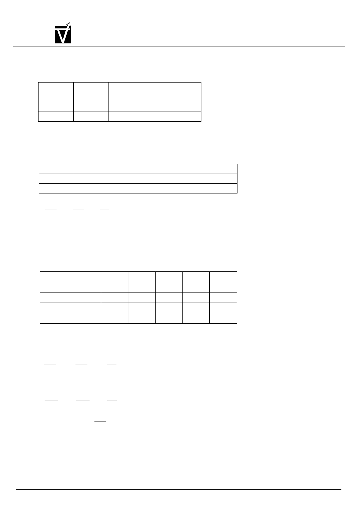
• Mode field (A8~A7)
A7 and A8 must be programmed to “00” in normal operation.
A8 A7 Test Mode
0 0 normal mode
0 1 Vendor Use Only
1 x Vendor Use Only
• Single Write Mode (A9)
This bit is used to select the write mode. When the A9 bit is “0”, Burst Read and Burst Write mode is
selected. When the A9 bit is ”1”, Burst Read and Single Write mode is Selected.
A9 Single Write Mode
0 Burst Read and Burst Write
1 Burst Read and Single Write
VG4616321B/VG4616322B
262,144x32x2-Bit
Preliminary CMOS Synchronous Graphic RAM
12 Special Mode Register Set command
(RAS = ”L”, CAS = ”L”, WE = ”L”, DSF = ”H”, BS, A0-A9 = Register Data)
The special mode register is used to load the Color and Mask registers, which are used in Block
Write and masked Write cycles. The control information being written to the Special Mode register is
applied to the address inputs and the data to be written to either the Color register or the Mask register is
applied to the DQs. When A6 is “high” during a Special Mode Register Set cycle, the Color register will be
loaded with the data on the DQs. Similarly, when A5 is “high” during a Special Mode Register Set cycle,
the Mask register will be loaded with the data on the DQs. A6 = A5 = 1 in the Special Mode Register Set
cycle is illegal.
Functions BS A9~A7 A6 A5 A4~A0
Leave Unchanged X X 0 0 X
Load Mask Register X X 0 1 X
Load Color Register X X 1 0 X
Illegal X X 1 1 X
One clock cycle is required to complete the write in the Special Mode register. This command can
be issued at the active state. As in write operation, this command accepts the data needed through DQ
pins. Therefore it should be attended not to induce bus contention.
13 No-Operation command
(RAS = ”H”, CAS = ”H”, WE = ”H”)
The No-Operation command is used to perform a NOP to SGRAM which is selected (CS is Low).
This prevents unwanted commands from being registered during idle or wait states.
14 Burst Stop command
(RAS = ”H”, CAS = ”H”, WE = ”L’, DSF = ”L”)
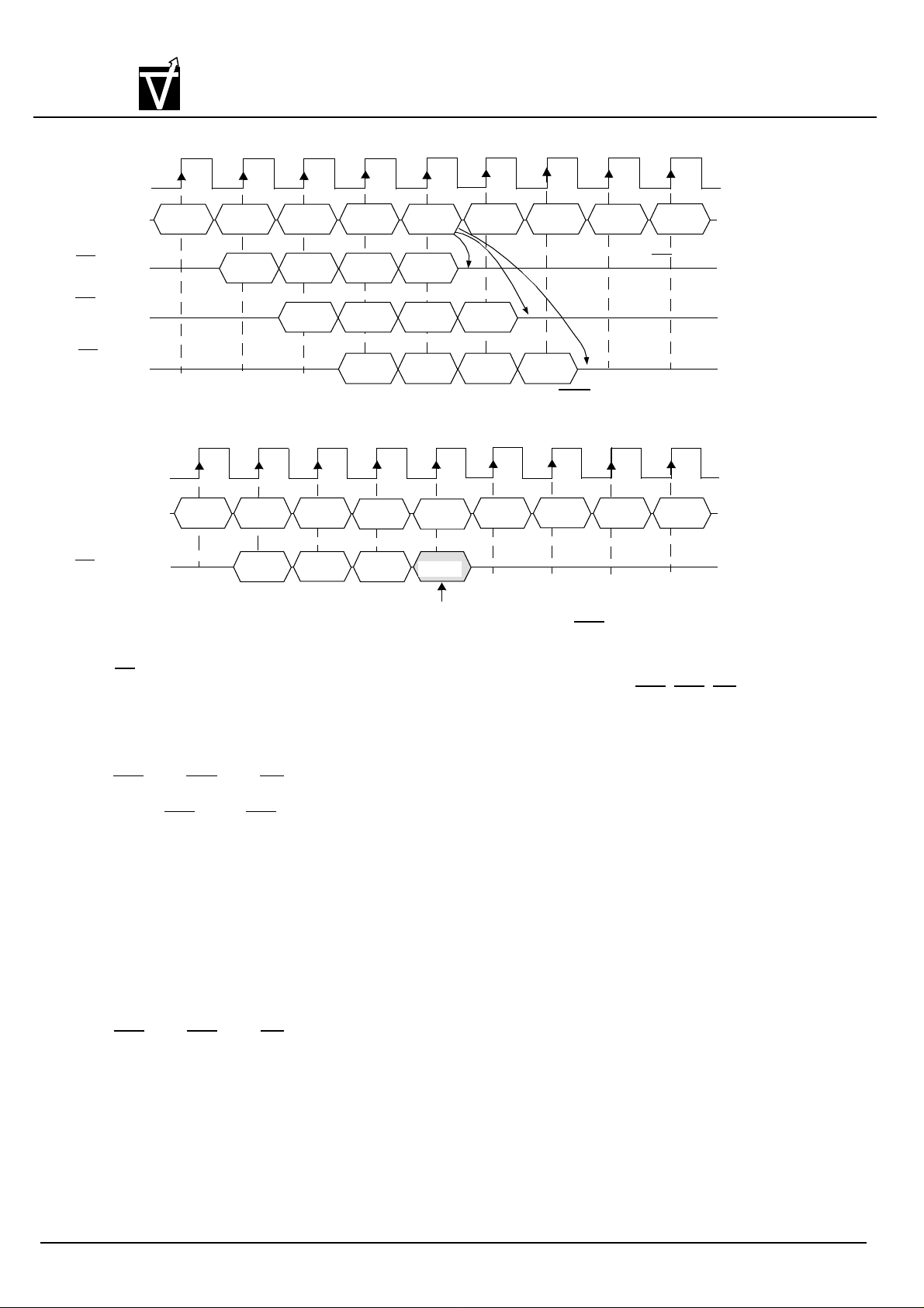
Burst Stop command is used to terminate either fixed-length or full-page bursts. This command is
only effective in a read/write burst without auto precharge function. The terminated read burst ends after
a delay equal to the CAS latency (refer to the following figure). The termination of a write burst is shown
in the following figure.
Document:1G5-0145 Rev.1 Page 18
Page 19
VIS
VG4616321B/VG4616322B
262,144x32x2-Bit
Preliminary CMOS Synchronous Graphic RAM
CLK
COMMAND
CAS Iatency = 1
t
,DQ’s
CK1
CAS Iatency = 2
t
,DQ’s
CK2
CAS Iatency = 3
t
,DQ’s
CK3
Termination of a Burst Write Operation (Burst Length > 4, CAS Latency = 1, 2, 3)
CLK
COMMAND
CAS latency = 1, 2, 3
DQ’s
NOP
T6
NOP
3
DOUT A
2
T6
NOP
3
T7 T8
NOP
T7 T8
NOP
NOP
NOP
T0
READ A
T0
NOP
T1
NOP
DOUT A
WRITE A
DIN A
T2
NOP
DOUT A
0
DOUT A
T1
T2
NOP
DIN A
0
T3
NOP
DOUT A
1
DOUT A
0
DOUT A
T3
NOP
DIN A
1
T4
Burst Stop
DOUT A
2
DOUT A
1
DOUT A
0
T4
Burst Stop
don’t care
2
Input data for the Write is masked.
T5
NOP
The burst ends after a delay equal to the CAS latency.
3
DOUT A
2
DOUT A
1
T5
Termination of a Burst Write Operation (Burst Length = X, CAS Latency = 1, 2, 3)
15 Device Deselect command
(CS = ”H”)
The Device Deselect command disables the command decoder so that the RAS, CAS, WE
and Address inputs are ignored, regardless of whether the CLK is enabled. This command is similar to the No Operation command.
16 AutoRefresh command (refer to Figures 3 & 4 in Timing Waveforms)
(RAS = ”L”, CAS = ”L”, WE = ”H”, DSF = ”L”, CKE = ”H”, BS, A0-A9 = Don’t care)
The AutoRefresh command is used during normal operation of the SGRAM and is anala-
gous to CAS-before-RAS(CBR) Refresh in conventional DRAMs. This command is non-persistent, so it must be issued each time a refresh is required. The addressing is generated by the
internal refresh controller. This makes the address bits a “don’t care” during an AutoRefresh
command. The internal refresh counter increments automatically on every auto refresh cycle to
all of the rows. The refresh operation must be performed 2048 times within 32ms. The time
required to complete the auto refresh operation is specified by tRP(min.). To provide the AutoRe-
fresh command, both banks need to be in the idle state and the device is not in power down
mode (CKE is high in the previous cycle). This command must be followed by NOPs until the
auto refresh operations is completed. The precharge time requirement, tRP(min.). must be met
befor successive auto refresh operations are performed.
17 SelfRefresh Entry command (refer to Figure 5 in Timing Waveforms)
(RAS = ”L”, CAS = ”L”, WE = ”H”, DSF = ”L”, CKE = ”L”, BS, A0-A9 = Don’t care)
The SelfRefresh is another refresh mode available in the SGRAM. It is the preferred refresh
mode for data retention and low power operation. Once the SelfRefresh command is registered,
all the inputs to the SGRAM becomes “don’t care” with the exception of CKE, which must remain
LOW. The refresh addressing and timing is internally generated to reduce power comsumption.
The SGRAM may remain in SelfRefresh mode for an indefinite period. Once the SGRAM enters
the SelfRefresh mode , t
(min.) is required before exit from SelfRefresh mode. The SelfRe-
RAS
fresh mode is exited by restarting the external clock and then asserting high on CKE(SelfRefresh
Exit command).
Document:1G5-0145 Rev.1 Page 19
Page 20

VG4616321B/VG4616322B
262,144x32x2-Bit
VIS
18 SelfRefresh Exit command (refer to Figure 5 in Timing Waveforms)
(CKE = ”H”, CS = ”H” or CKE = ”H”, RAS = ”H”, CAS = ”H”, WE = ”H”)
NOP or Device Deselect commands must be issued for tRC(min), because time is required for the
completion of any bank currently being internally refreshed. If auto refresh cycles in bursts are performed during normal operation, a burst of 1024 auto refresh cycles should be completed just prior to
entering, and just after exiting the SelfRefresh mode.
19 Clock Suspend Mode Entry/PowerDown Mode Entry command (refer to Figures 6, 7, and 8 in Timing
Waveforms)
(CKE = ”L”)
sequent cycle by issuing this command (asserting CKE ”low”). The device operation is held intact
while CLK is suspended. On the other hand, when both banks are in the idle state, this command performs entry into the PowerDown mode. All input and output buffers (except the CKE buffer) are turned
off in the PowerDown mode. The device may not remain in the Clock Suspend or PowerDown state
longer than the refresh period (16ms) since the command does not perform any refresh operations.
20 Clock Suspend Mode Exit/PowerDown Mode Exit command (refer to Figures 6, 7, and 8 in Timing
Waveforms)
(CKE = ”H”)
the subsequent cycle by providing this command (asserting CKE “high”). When the device is in the
PowerDown mode, the device exits this mode and all disabled buffers are turned on to the active
state. t
mands can be issued after one clock cycle from the end of this command.
Preliminary CMOS Synchronous Graphic RAM
The command is used to exit from the SelfRefresh mode. Once this command is registered,
When SGRAM operating the burst cycle, the internal CLK is suspended (masked) from the sub-
When the internal CLK has been suspended, the operation of the internal CLK is resumed from
(min.) is required when the device exit from the PowerDown mode. Any subsequent com-
PDE
21 Data Write/Output Enable, Data Mask/Output Disable command
(DQM = ”L”, ”H”)
During a write cycle, the DQM signal functions as Data Mask and can control every word of the
input data. During a read cycle, the DQM functions as the control of output buffers. DQM is also used
for device selection, byte selection and bus control in a memory system. DQM0 controls DQ0 to DQ7,
DQM1 controls DQ8 to DQ15, DQM2 controls DQ16 to DQ23, DQM3 controls DQ24 to DQ31, DQM
masks the DQ’s by a byte regardless that the corresponding DQ’s are in a state of write-per-bit masking or pixel masking. the byte control. The each DQM0-3 corresponds to DQ0-7, DQ8-15, DQ16-23,
DQ24-31.
Document:1G5-0145 Rev.1 Page 20
Page 21
VG4616321B/VG4616322B
262,144x32x2-Bit
VIS
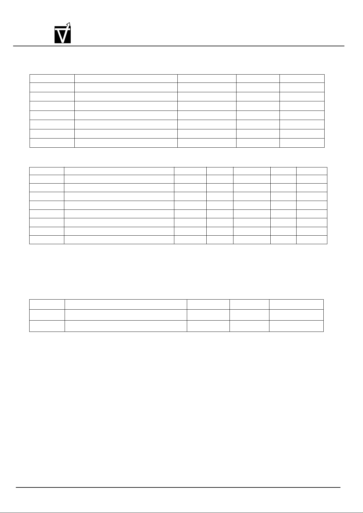
Absolute Maximum Rating
Symbol Item Rating Unit Note
VIN, V
OUT
VDD, V
T
OPR
T
STG
T
SOLDER
P
D
I
OUT
Recommended D.C. Operating Conditions (Ta = 0~70°C)
Symbol Parameter Min. Typ. Max. Unit Note
V
DD
V
DDQ
V
IH
V
IL
V
ref
V
IH
V
IL
V
TT
Preliminary CMOS Synchronous Graphic RAM
Input, Output Voltage -0.3~VDD + 0.3 V 1
DDQ
Power Supply Voltage (for I/O Buffer) 3.0 3.3 3.6 V 2
Power Supply Voltage -0.3~4.6 V 1
Operating Temperature 0~70 °C 1
Storage Temperature -55~150 °C 1
Soldering Temperature(10s) 260 °C 1
Power Dissipation 1 W 1
Short Circuit Output Current 50 mA 1
Power Supply Voltage 3.0 3.3 3.6 V 2
LVTTL Input High Voltage 2.0 - VDD+ 0.3 V 2
LVTTL Input LOW Voltage -0.3 - 0.8 V 2
Input Reference Voltage 1.25 1.5 1.75 V 2
SSTL Input High voltage V
SSTL Input Low Voltage -0.3 - V
SSTK Teruination Voltage V
+0.2 - V
REF
-0.1 V V
REF
+0.3 V 2
DDQ
+0.2 V 2
REF
+0.1 V 2
REF
Note : the peak to peak AC noise on Vref may not exceed 2%. V
must track V
the transmitting device and V
of receiving device. Typically the value of V
REF
track Variations in V
REF
DDQ
(DC). Vtt of transmitting device
REF
must be about 0.45 * V
REF
.
DDQ
of
Capacitance (VDD = 3.3V, f = 1MHz, Ta = 25°C)
Symbol Parameter Min. Max. Unit
C
I
C
I/O
Note: These parameters are periodically sampled and are not 100% tested.
Input Capacitance - 5 pF
Input/Output Capacitance - 7 pF
Document:1G5-0145 Rev.1 Page 21
Page 22
VIS
VG4616321B/VG4616322B
262,144x32x2-Bit
Preliminary CMOS Synchronous Graphic RAM
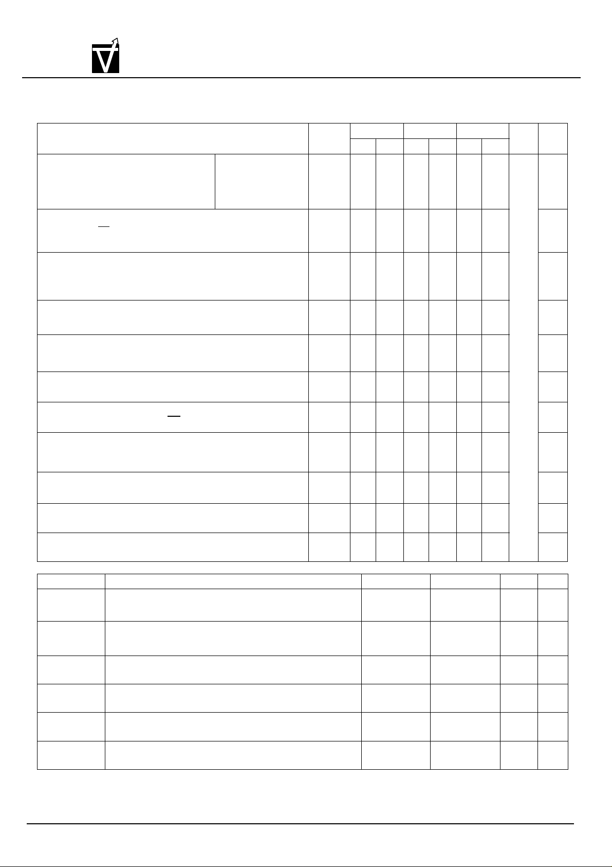
Recommended D.C. Operating Conditions (VDD = 3.3V 0.3V, Ta = 0 ~ 70¢J)
±
-5 -6 -7 Unit Note
Description/test condition Symbol
Operating Current
t
t
≥
, Outputs Open
RC
RCmin
()
Address changed once during t
CK(min)
.
1 bank
operation
I
DD1
Min.Max.Min.Max.Min.Max.
190 170 150
Burst Length = 1
Precharge Standby Current in non-power down mode
t
CK
= t
CK(min)
CSV
,
≥ CKEV
(min)
IH
,
≥
IH
(min)
I
DD2N
35 35 35 3
Input signals are changed once during 30ns.
Precharge Standby Current in non-power down mode
∞ CKEV
= ,
t
CK
≥ CLKV
,
(min)
IH
≤
(max)
IL
I
DD2NS
15 15 15
Input signals are stable
Precharge Standby Current in power down mode
t
= tCK(min),
CK
CKEVIL≤
(max)
Precharge Standby Current in power down mode
∞CKEV
= ,
t
CK
≤ CLKV
IL
(max)
,
≤
(max)
IL
Active Standby Current in non power down mode
, t
CKEV
≥
(min)
IH
CK
= t
CK(min)
Active Standby Current in power down mode
CKEV
≤ ≥
IL
(max)
, t
CK = tCK(min)
, CS V
IH(min)
Operating Current (Page Burst, and All Bank activated)
t
CCD
= t
CCD(min)
, Outputs Open, Multi-bank interleave, gapless
I
DD2P
I
DD2PS
I
DD3P
I
DD3N
I
DD4
2.0 2.0 2.0 3
2.0 2.0 2.0
4 4 4 3
30 30 30
220 200 170 4,5
data
Refresh Current
t
≥
RCtRC
(min)
Self Refresh Current I
≤
CKE0.2V
Operating Current (Block Write)
t
CK
= t
, Outputs Open, t
CK(min)
BWC
= t
BWC(min)
I
DD5
DD6
I
DD7
190 170 140 3
1 1 1
250 230 190
3,4
mA
Parameter Description Min. Max. Unit Note
I
IL
I
OL
(All other pins not under test = OV)
0VVINV
≤≤
Output disable, ()
V
OH
V
OL
V
OH
V
OL
Input Leakage Current
DD
Output Leakage Current
0VV
≤≤
OUTVDDQ
LVTTL Output ”H” Level Voltage
(l
= -2mA)
OUT
LVTTL Output ”L” Level Voltage
(l
= 2mA)
OUT
SSTL Output ”H” Level Voltage
(l
= -16mA)
OUT
SSTL Output ”L” Level Voltage
(l
= 16mA)
OUT
-5 5 A
-5 5 A
2.4 - V
- 0.4 V
+0.8 - V
V
TT
- V
+0.8 V
TT
Document:1G5-0145 Rev.1 Page 22
µ
µ
Page 23

VG4616321B/VG4616322B
±
262,144x32x2-Bit
VIS
Electrical Characteristics and Recommended A.C. Operating Conditions
(VDD = 3.3V0.3V, Ta = 0~70°C) (Note: 6, 7, 8, 9, 10) *** CL is CAS Latency.
symbol A.C. Parameter -5 -6 -7
t
RC
t
RCD
t
RP
t
RRD
t
RAS
t
WR
t
CK1
t
CK2
t
CK3
t
CH
t
CL
t
AC1
t
AC2
t
AC3
t
T
t
CCD
t
OH
t
LZ
t
HZ1
t
HZ2
t
HZ3
t
IS
t
IH
t
SRX
t
PDE
t
RSC
t
BWC
t
DAL2
t
DAL3
t
BPL
t
REF
Row cycle time 45 54 62
RAS to CAS delay 15 18 20
Precharge to refresh/row activate com-
mand
Row activate to row activate delay 10 12 14
Row activate to precharge time 30 100,000 36 100,000 40 100,000
Write recovery time 1 1 1 CLK
Clock cycle time
Clock high time 1.5 2 2.5
Clock low time 1.5 2 2.5
Access time from CLK
(positive edge)
Transition time of CLK (Rise and Fall) 0.5 10 0.5 10 0.5 10
CAS to CAS Delay time 1 1 1 CLK
Data output hold time 2 2.5 2.5
Data output low impedance 2 2 2
Data output high impedance
Data/Address/Control Input setup time 1 1 1.5
Data/Address/Control Input hold time 1 1 1
Minimum CKE ”High”for Self-Refresh exit 1 1 1 CLK
Power Down Exit set-up time 3 4 5 ns
(Special) Mode Register Set Cycle time 2 2 2 CLK
Block Write Cycle time 1 1 1 CLK
Data-in to ACT Command
Block Write to Precharge command 1 1 1 CLK
Refresh time 32 32 32 ms
Preliminary CMOS Synchronous Graphic RAM
Min. Max. Min. Max. Min. Max.
15 18 20
CL* = 1 14 16 18
7 8 9
5 6 7
CL* = 1 11 13 15
CL* = 2 5 5 6
CL* = 3 4.5 5 5.5
CL = 1 3 5 3 5 3 6
CL = 2 3 5 3 5 3 6
CL = 3 3 5 3 5 3 5
(CL = 2)
(CL = 3)
1clk
+t
1clk
+t
RP
RP
1clk+
t
RP
1clk+
t
RP
1clk
+t
1clk
+t
unit
ns
ns
ns
RP
RP
Document:1G5-0145 Rev.1 Page 23
Page 24

VG4616321B/VG4616322B
262,144x32x2-Bit
VIS
Note:
1. Stresses greater than those listed under “Absolute Maximum Ratings” may cause permanent damage to the
device.
2. All voltages are referenced to VSS.
3. These parameters depend on the cycle rate and these values are measured by the cycle rate under the minimum
value of tCK and tRC. Input signals are changed one time during tCK. Assume that there are only one read/write
cycle during tRC (min).
4. These parameters depend on the output loading. Specified values are obtained with the output open.
5. Assume minimum column address update cycle t
6. Power-up sequence is described in Note 11.
7. A.C. Test Conditions
Reference Level of Output Signals 1.4V / 1.4V
Preliminary CMOS Synchronous Graphic RAM
(min).
CCD
Output Load Reference to the Under Output Load (B)
Input Signal Levels 3.0V / 0.0V
Transition Time (Rise and Fall) of Input Signals 1ns
Reference Level of Input Signals 1.4V
3.3V
1.2K
Ω
ZO=50
Output
30pF
LVTTL D.C. Test Load (A)
870
Output
Ω
LVTTL A.C. Test Load (B)
Ω
1.4V
50
30pF
Ω
Document:1G5-0145 Rev.1 Page 24
Page 25
VG4616321B/VG4616322B
262,144x32x2-Bit
VIS
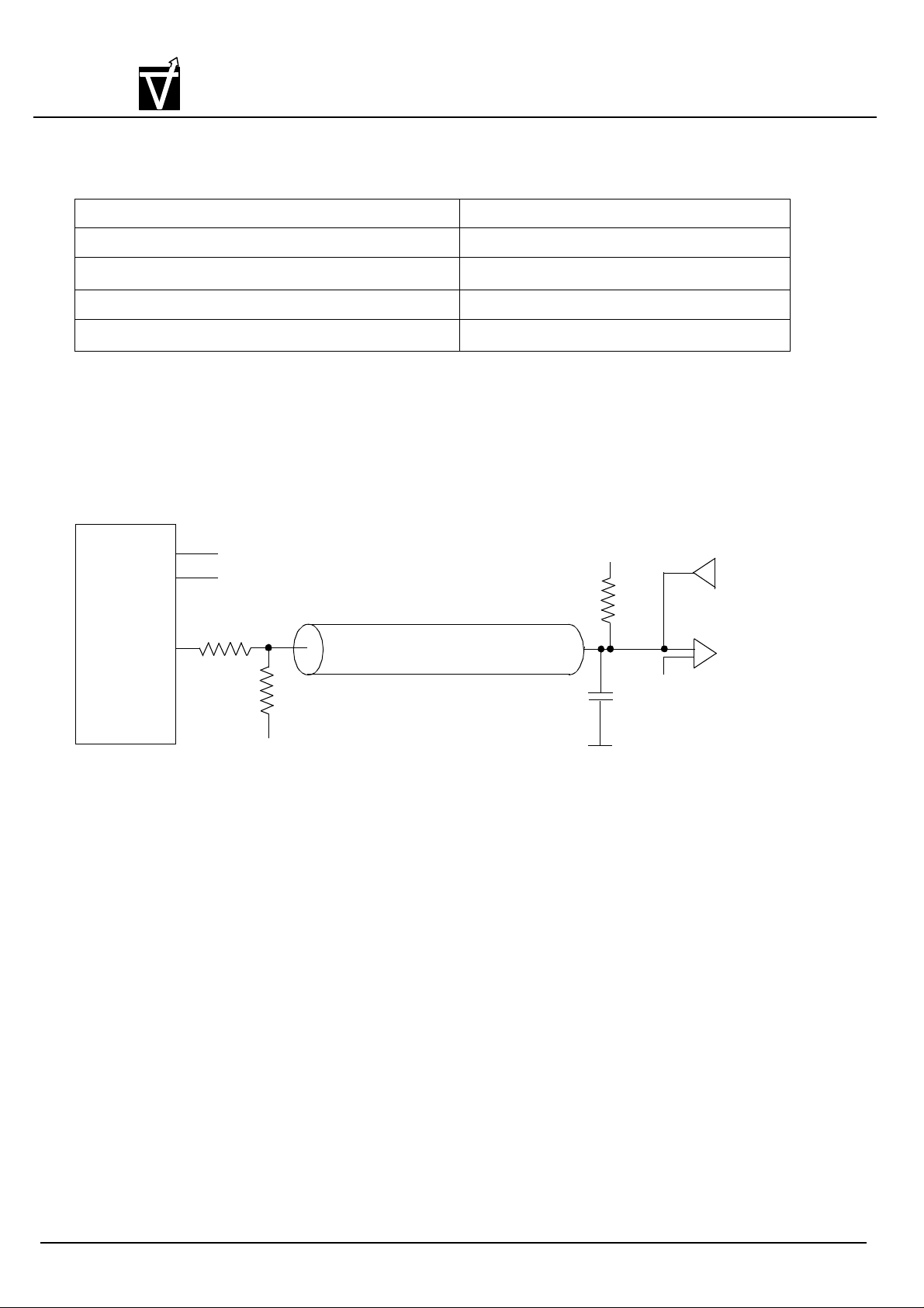
SSTL_3 Interface
Reference Level of Output Signals (VREF) 0.45*VDDQ
Output Load Reference to the Under Output Load
Preliminary CMOS Synchronous Graphic RAM
Input Signal Levels V
Transition Time (Rise and Fall) of Input Signals 1ns
Reference Level of Input Signals(V
) 0.45*V
REF
AC Test Load Circuits (for SSTL - 3 interface) :
Device
Under
Test
V
V
V
DDQ
REF
OUT
V
DDQ
0.45 * V
RS = 25 Ohms
VTT = 0.45 * V
DDQ
Z = 50 Ohms
RT1 = 50 Ohms
DDQ
+ 0.4/V
REF
RT2 = 50 Ohms
C
LOAD
REF
DDQ
VTT = 0.45 * V
= 30 pF
-0.4
DDQ
V
IN
V
= 0.45 * V
REF
V
SS
DD
SSTL-3 A.C. Test Load
8. Transition times are measured between VIH and VIL. Transition (rise and fall) of input signals are fixed slope (1 ns).
9. t
defines the time at which the outputs achieve the open circuit condition and are not reference levels.
OHZ
10. These parameters account for the number of clock cycle and depend on the operating frequency of the clock, as
follows:
the number of clock cycles = specified value of timing/Clock cycle time (count fractions as a whole number)
Document:1G5-0145 Rev.1 Page 25
Page 26

VG4616321B/VG4616322B
262,144x32x2-Bit
VIS
Latency relationship to frequency (Unit : clock cycles)
-5 Version (Calculation with t
Clock period
(tCK)
30ns 2 1 1 1 1 1
20ns 3 1 1 2 1 1
15ns 3 1 1 2 1 1
10ns 5 2 1 3 1 2
5ns 9 3 2 6 2 3
Preliminary CMOS Synchronous Graphic RAM
= 5ns ~ 30ns)
CK
t
RC
45 15 10 30 10 15
t
RP
t
RRD
t
RAS
t
RSC
t
RCD
-6 Version (Calculation with t
Clock period
(tCK)
30ns 2 1 1 2 1 1
20ns 3 1 1 2 1 1
15ns 4 2 1 3 1 2
10ns 6 2 2 4 2 2
6ns 9 3 2 6 2 3
-7 Version (Calculation with t
Clock period
(tCK)
30ns 3 1 1 2 1 1
20ns 4 1 1 2 1 1
15ns 5 2 1 3 1 2
10ns 7 2 2 4 2 2
7ns 9 3 2 6 2 3
11. Power up Sequence
Power up must be performed in the following sequence.
1) Power must be applied to VDD and V
state and CKE = ”H”, DQM = ”H”. The CLK signals must be started at the same time.
2) After power-up, a pause of 200u secouds minimum is required. Then, it is recommended that
DQM is held “high” (VDD levels) to ensure DQ output to be in the high impedance.
= 6ns ~ 30ns)
CK
t
RC
54 18 12 36 12 18
= 7ns ~ 30ns)
CK
t
RC
62 20 12 36 14 20
t
RP
t
RP
DDQ
t
RRD
t
RRD
(simultaneously) when all input signals are held “NOP”
t
t
RAS
RAS
t
RSC
t
RSC
t
RCD
t
RCD
3) Both banks must be precharged.
4) Mode Register Set command must be asserted to initialize the Mode register.
5) A minimum of 8 Auto-Refresh dummy cycles must be required to stabilize the internal circuitry of
the device. Sequence of 4 and 5 may be changed.
Document:1G5-0145 Rev.1 Page 26
Page 27
VG4616321B/VG4616322B
262,144x32x2-Bit
VIS
Timing Waveforms
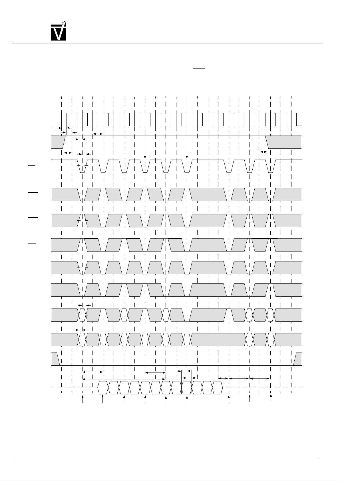
Figure 1. AC Parameters for Write Timing (Burst Length = 4, CAS Latency = 2)
Preliminary CMOS Synchronous Graphic RAM
T0 T1 T2 T3 T4 T5 T6 T7 T8 T9 T10 T11 T12 T13 T14 T15 T16 T17 T18 T19 T20 T21 T22
CLK
CKE
CS
RAS
CAS
WE
DSF
BS
t
CH
t
CL
t
IS
t
CK2
t
IS
t
IH
Begin Auto Precharge
Bank A
Begin Auto Precharge
Bank B
t
IS
t
IH
A9
A0 ~ A8
DQM
DQ
Hi-Z
RAx
t
IS
RBx
Activate
Command
Bank A
CAx
t
RCD
t
RC
Ax0 Ax1
Write with
Auto Precharge
Command
Bank A
RBx
RBx CBx
Ax2 Ax3 Bx0 Bx1
Activate
Command
Bank B
Write with
Auto Precharge
Command
Bank B
RAy RAz
CAy RAz
t
IS
Ay0 Ay1
Write
Command
Bank A
t
IH
Ay2
Ay3
t
WR
Command
Precharge
Bank A
t
DAL
RAy
Bx2 Bx3
Activate
Command
Bank A
t
RP
Activate
Command
Bank A
t
RRD
RBy
RBy
Activate
Command
Bank B
Document:1G5-0145 Rev.1 Page 27
Page 28
VG4616321B/VG4616322B
262,144x32x2-Bit
VIS
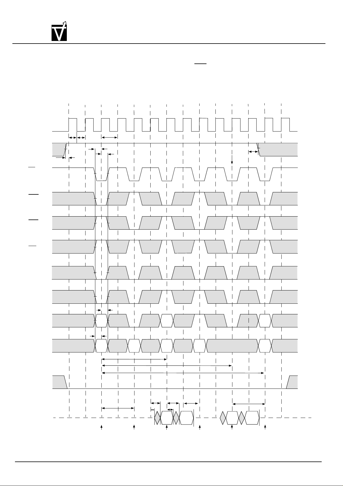
Figure 2. AC Parameters for Read Timing (Burst Length = 2, CAS Latency = 2)
Preliminary CMOS Synchronous Graphic RAM
T0 T1 T2 T3 T4 T5 T6 T7 T8 T9 T10 T11 T12 T13
CLK
CKE
CS
RAS
CAS
WE
DSF
BS
tCHt
CL
t
IS
t
CK2
t
IS
t
IH
Begin Auto Precharge
Bank B
t
IH
t
IH
A9
A0 ~ A8
RAx
t
IS
t
RRD
CAx
RAx
RBx RAy
RBx
t
RAS
t
RC
RAyCBx
DQM
t
DQ
Hi-Z
Activate
Command
Bank A
t
RCD
Read
Command
Bank A
t
AC2
t
LZ
AC2
t
OH
Ax0
Activate
Command
Bank B
t
HZ
Ax1
Read with
Auto Precharge
Command
Bank B
Bx0
Precharge
Command
Bank A
t
RP
Bx1
Activate
Command
Bank A
Document:1G5-0145 Rev.1 Page 28
Page 29

VG4616321B/VG4616322B
262,144x32x2-Bit
VIS
Figure 3. Auto Refresh (CBR) (Burst Length = 4, CAS Latency = 2)
Preliminary CMOS Synchronous Graphic RAM
T0 T1 T2 T3 T4 T5 T6 T7 T8 T9 T10 T11 T12 T13 T14 T15 T16 T17 T18 T19 T20 T21 T22
CLK
CKE
CS
RAS
CAS
WE
DSF
t
CK2
BS
A9
A0 ~ A8
t
RP
t
RC
t
RC
RAx
RAx
CAx
DQM
DQ
Hi-Z
Precharge All
Command
Auto Refresh
Command
Auto Refresh
Command
Activate
Command
Bank A
Read
Command
Bank A
Ax0
Ax1 Ax2 Ax3
Document:1G5-0145 Rev.1 Page 29
Page 30

VG4616321B/VG4616322B
262,144x32x2-Bit
VIS
Figure 4. Power on Sequence and Auto Refresh (CBR)
Preliminary CMOS Synchronous Graphic RAM
T0 T1 T2 T3 T4 T5 T6 T7 T8 T9 T10 T11 T12 T13 T14 T15 T16 T17 T18 T19 T20 T21 T22
CLK
CKE
CS
RAS
CAS
WE
DSF
BS
t
CK2
High level
is required
Minimum of 8 Refresh cycles are required
2 Clock min.
A9
Address Key
A0 ~ A8
DQM
t
RC
Mode Register
Set Command
Any
Command
DQ
Hi-Z
Precharge All
Command
Inputs must be
stable for 200 us
t
RP
1st Auto Refresh
Command
2nd Auto Refresh
Command
Document:1G5-0145 Rev.1 Page 30
Page 31
VG4616321B/VG4616322B
262,144x32x2-Bit
VIS
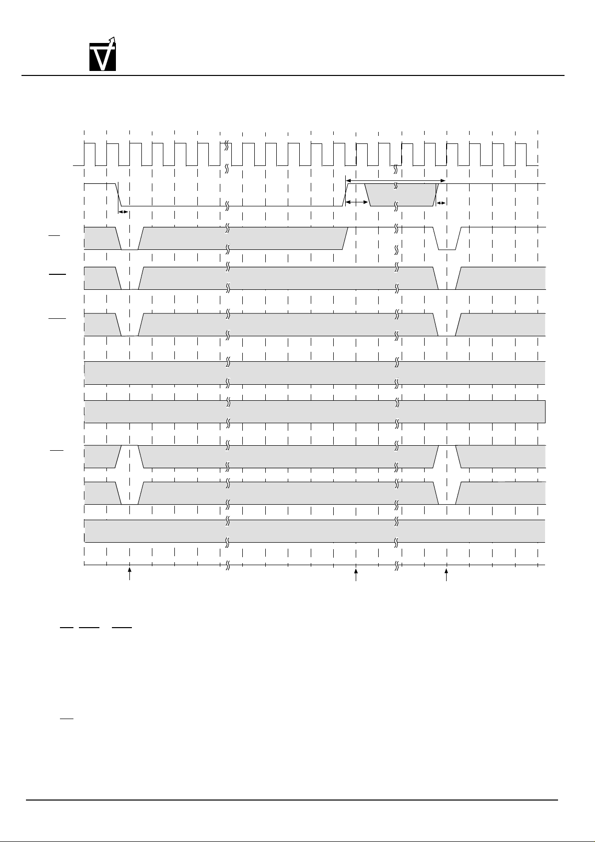
Figure 5. Self Refresh Entry & Exit Cycle
Preliminary CMOS Synchronous Graphic RAM
T0 T1 T2 T3 T4 T5 T6 T7 T8 T9 T10 T11 T12 T13 T14 T15 T16 T17 T18 T19
CLK
CKE
CS
RAS
CAS
BS
A0 ~ A9
* Note 1
* Note 8
* Note 2
* Note 3
t
IS
* Note 4
t
SRX
* Note 5
* Note 6
t
RC(min)
* Note 7
t
PDE
* Note 8
WE
DSF
DQM
DQ
Hi-Z
Self Refresh Enter
Hi-Z
Self Refresh Exit
Auto Refresh
Note: To Enter SelfRefresh Mode
1. CS, RAS & CAS with CKE should be low at the same clock cycle.
2. After 1 clock cycle, all the inputs including the system clock can be don’t care except for CKE.
3. The device remains in SelfRefresh mode as long as CKE stays “low”.
Once the device enters SelfRefresh mode, Minimum t
is required before exit from SelfRefresh.
RAS
Note: To Exit SelfRefresh Mode
4. System clock restart and be stable before returning CKE high.
5. Enable CKE and CKE should be set high for minimum time of t
SRX
.
6 .CS starts from high.
7. Minimum tRC is required after CKE going high to complete SelfRefresh exit.
8. 1024 cycles of burst AutoRefresh is required before SelfRefresh entry and after SelfRefresh exit if the
system uses burst refresh.
Document:1G5-0145 Rev.1 Page 31
Page 32
VG4616321B/VG4616322B
262,144x32x2-Bit
VIS
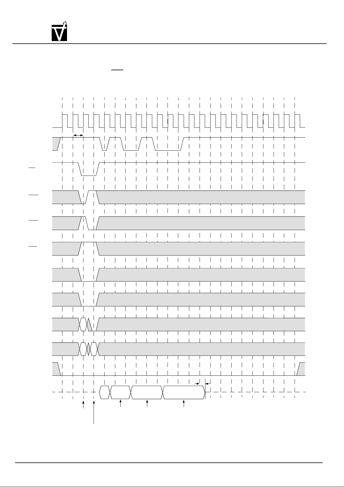
Figure 6.1 Clock Suspension During Burst Read (Using CKE)
(Burst Length = 4, CAS Latency = 1)
Preliminary CMOS Synchronous Graphic RAM
T0 T1 T2 T3 T4 T5 T6 T7 T8 T9 T10 T11 T12 T13 T14 T15 T16 T17 T18 T19 T20 T21 T22
CLK
CKE
CS
RAS
CAS
WE
BS
t
CK1
BS
A9
A0 ~ A8
DQM
DQ
Note: CKE to CLK disable/enable = 1 clock
Hi-Z
RAx
RAx CAx
Activate
Command
Bank A
Command
Bank A
Read
Ax0
Ax1
Clock Suspend
1 Cycle
Ax2
Clock Suspend
2 Cycles
t
HZ
Ax3
Clock Suspend
3 Cycles
Document:1G5-0145 Rev.1 Page 32
Page 33

VG4616321B/VG4616322B
262,144x32x2-Bit
VIS
Figure 6.2 Clock Suspension During Burst Read (Using CKE)
(Burst Length = 4, CAS Latency = 2)
Preliminary CMOS Synchronous Graphic RAM
T0 T1 T2 T3 T4 T5 T6 T7 T8 T9 T10 T11 T12 T13 T14 T15 T16 T17 T18 T19 T20 T21 T22
CLK
CKE
CS
RAS
CAS
WE
DSF
t
CK2
BS
Hi-Z
RAx
RAx CAx
Activate
Command
Bank A
Read
Command
Bank A
Ax0
Ax1
Clock Suspend
1 Cycle
Ax2
Clock Suspend
2 Cycles
t
HZ
Ax3
Clock Suspend
3 Cycles
A9
A0 ~ A8
DQM
DQ
Note: CKE to CLK disable/enables = 1 clock
Document:1G5-0145 Rev.1 Page 33
Page 34
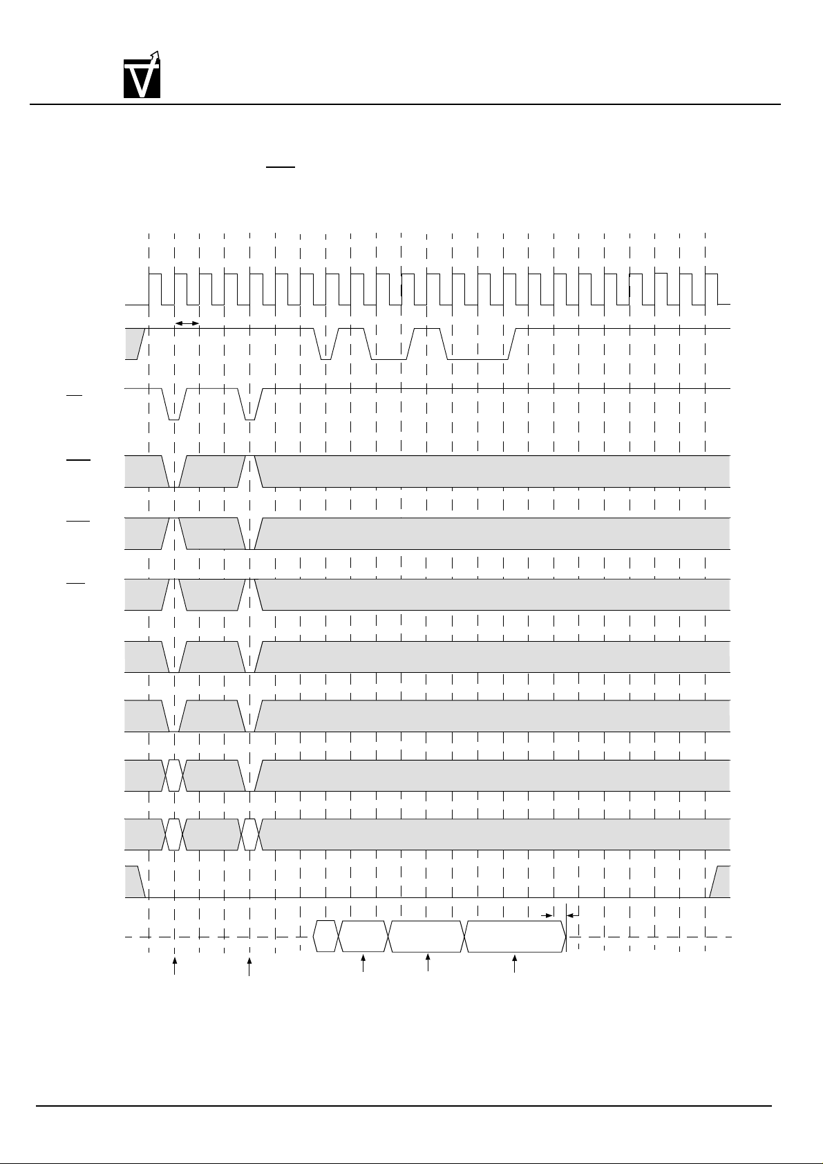
VG4616321B/VG4616322B
262,144x32x2-Bit
VIS
Figure 6.3 Clock Suspension During Burst Read (Using CKE)
(Burst Length = 4, CAS Latency = 3)
Preliminary CMOS Synchronous Graphic RAM
T0 T1 T2 T3 T4 T5 T6 T7 T8 T9 T10 T11 T12 T13 T14 T15 T16 T17 T18 T19 T20 T21 T22
CLK
CKE
CS
RAS
CAS
WE
DSF
t
CK3
BS
A9
A0 ~ A8
RAx
RAx CAx
DQM
DQ
Note: CKE to CLK disable/enable = 1 clock
Hi-Z
Activate
Command
Bank A
Read
Command
Bank A
Ax0
Ax1
Clock Suspend
1 Cycle
Ax2
Clock Suspend
2 Cycles
t
HZ
Ax3
Clock Suspend
3 Cycles
Document:1G5-0145 Rev.1 Page 34
Page 35
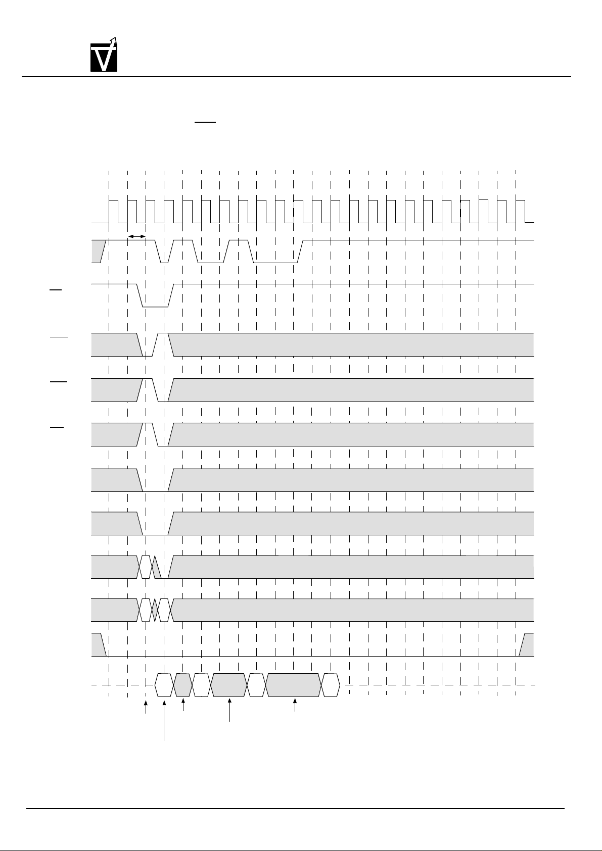
VG4616321B/VG4616322B
262,144x32x2-Bit
VIS
Figure 7.1 Clock Suspension During Burst Write (Using CKE)
(Burst Length = 4, CAS Latency = 1)
Preliminary CMOS Synchronous Graphic RAM
T0 T1 T2 T3 T4 T5 T6 T7 T8 T9 T10 T11 T12 T13 T14 T15 T16 T17 T18 T19 T20 T21 T22
CLK
CKE
CS
RAS
CAS
WE
DSF
t
CK1
BS
A9
A0 ~ A8
RAx
RAx CAx
DQM
DQ
Note: CKE to CLK disable/enable = 1 clock
Hi-Z
Activate
Command
Bank A
Command
Bank A
DAx0
Clock Suspend
1 Cycle
Write
DAx1 DAx2 DAx3
Clock Suspend
Clock Suspend
2 Cycles
3 Cycles
Document:1G5-0145 Rev.1 Page 35
Page 36

VG4616321B/VG4616322B
262,144x32x2-Bit
VIS
Figure 7.2 Clock Suspension During Burst Write (Using CKE)
(Burst Length = 4, CAS Latency = 2)
Preliminary CMOS Synchronous Graphic RAM
T0 T1 T2 T3 T4 T5 T6 T7 T8 T9 T10 T11 T12 T13 T14 T15 T16 T17 T18 T19 T20 T21 T22
CLK
CKE
CS
RAS
CAS
WE
DSF
t
CK2
BS
A9
A0 ~ A8
RAx
RAx CAx
DQM
DQ
Note: CKE to CLK disable/enable = 1 clock
Hi-Z
Activate
Command
Bank A
Command
Bank A
DAx0
Clock Suspend
1 Cycle
Write
DAx1 DAx2 DAx3
Clock Suspend
Clock Suspend
2 Cycles
3 Cycles
Document:1G5-0145 Rev.1 Page 36
Page 37
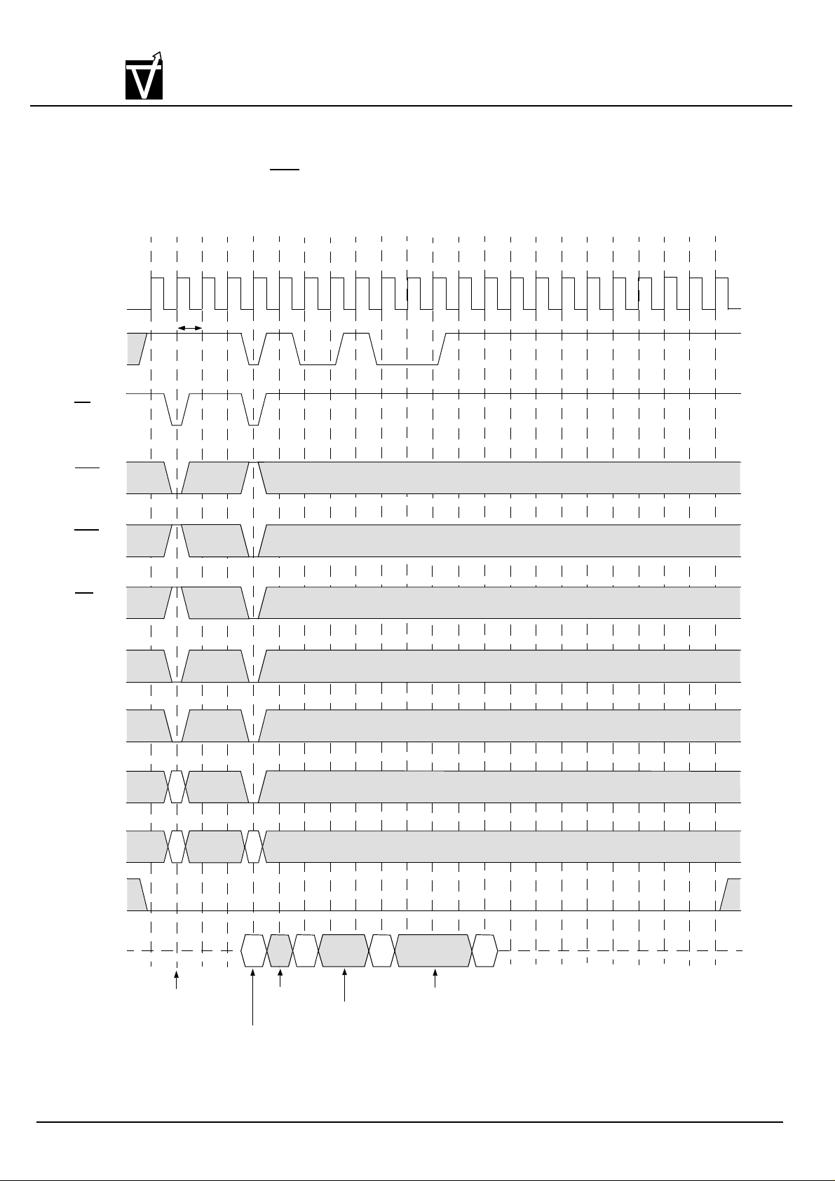
VG4616321B/VG4616322B
262,144x32x2-Bit
VIS
Figure 7.3 Clock Suspension During Burst Write (Using CKE)
(Burst Length = 4, CAS Latency = 3)
Preliminary CMOS Synchronous Graphic RAM
T0 T1 T2 T3 T4 T5 T6 T7 T8 T9 T10 T11 T12 T13 T14 T15 T16 T17 T18 T19 T20 T21 T22
CLK
CKE
CS
RAS
CAS
WE
DSF
t
CK3
BS
A9
A0 ~ A8
RAx
RAx CAx
DQM
DQ
Note: CKE to CLK disable/enable = 1 clock
Hi-Z
Activate
Command
Bank A
DAx0
Clock Suspend
1 Cycle
Write
Command
Bank A
DAx1 DAx2 DAx3
Clock Suspend
Clock Suspend
2 Cycles
3 Cycles
Document:1G5-0145 Rev.1 Page 37
Page 38
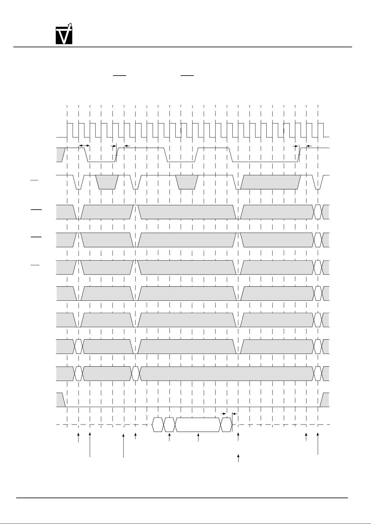
VG4616321B/VG4616322B
262,144x32x2-Bit
VIS
Figure 8. Power Down Mode and Clock Mask
(Burst Length = 4, CAS Burst Length = 4, CAS Latency = 2)
Preliminary CMOS Synchronous Graphic RAM
T0 T1 T2 T3 T4 T5 T6 T7 T8 T9 T10 T11 T12 T13 T14 T15 T16 T17 T18 T19 T20 T21 T22
CLK
CKE
CS
RAS
CAS
WE
DSF
t
CK2
t
IS
Valid
t
PDE
BS
A9
A0 ~ A8
RAx
RAx CAx
DQM
tHZ
DQ
Hi-Z
Activate
Command
Bank A
Power Down
Mode Entry
ACTIVE
STANDBY
Read
Command
Bank A
Power Down
Mode Exit
Ax0
Ax1
Clock Mask
Start
Ax2
Clock Mask
End
Ax3
Precharge
Command
Bank A
Power Down
Mode Entry
PRECHARGE
STANDBY
Power Down
Mode Exit
Command
Document:1G5-0145 Rev.1 Page 38
Any
Page 39
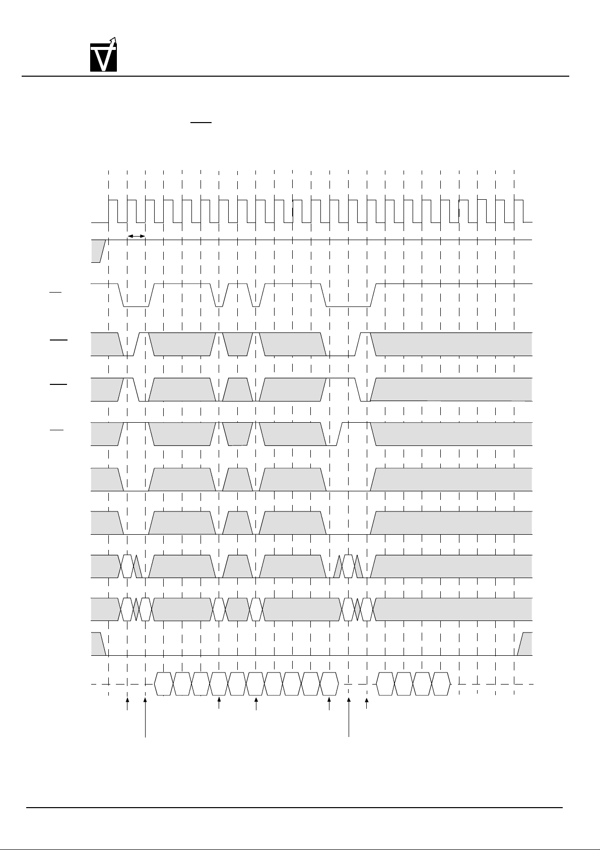
VG4616321B/VG4616322B
262,144x32x2-Bit
VIS
Figure 9.1 Random Column Read (Page within same Bank)
(Burst Length = 4, CAS Latency = 1)
Preliminary CMOS Synchronous Graphic RAM
T0 T1 T2 T3 T4 T5 T6 T7 T8 T9 T10 T11 T12 T13 T14 T15 T16 T17 T18 T19 T20 T21 T22
CLK
CKE
CS
RAS
CAS
WE
DSF
t
CK1
BS
A9
A0 ~ A8
RAw
RAw
CAw
CAx CAy
RAz
RAz
CAz
DQM
DQ
Hi-Z
Activate
Command
Bank A
Command
Bank A
Read
Aw1
Aw2
Aw3 Ax0 Ax1 Ay0
Read
Command
Bank A
Read
Command
Bank A
Ay1
Ay2
Precharge
Command
Bank A
Ay3
Activate
Command
Bank A
Read
Command
Bank A
Az0 Az1
Az2
Az3Aw0
Document:1G5-0145 Rev.1 Page 39
Page 40

VG4616321B/VG4616322B
262,144x32x2-Bit
VIS
Figure 9.2 Random Column Read (Page within same Bank)
(Burst Length = 4, CAS Latency = 2)
Preliminary CMOS Synchronous Graphic RAM
T0 T1 T2 T3 T4 T5 T6 T7 T8 T9 T10 T11 T12 T13 T14 T15 T16 T17 T18 T19 T20 T21 T22
CLK
CKE
CS
RAS
CAS
WE
DSF
t
CK2
BS
A9
A0 ~ A8
RAw
RAw
CAW
CAx CAy
RAz
RAz
CAz
DQM
DQ
Hi-Z
Activate
Command
Bank A
Read
Command
Bank A
Aw0
Aw3
Read
Command
Bank A
Ax0 Ax1 Ay0
Read
Command
Bank A
Ay1
Ay2 Ay3Aw1 Aw2
Precharge
Command
Bank A
Activate
Command
Bank A
Read
Command
Bank A
Az0
Az1
Az2
Document:1G5-0145 Rev.1 Page 40
Az3
Page 41
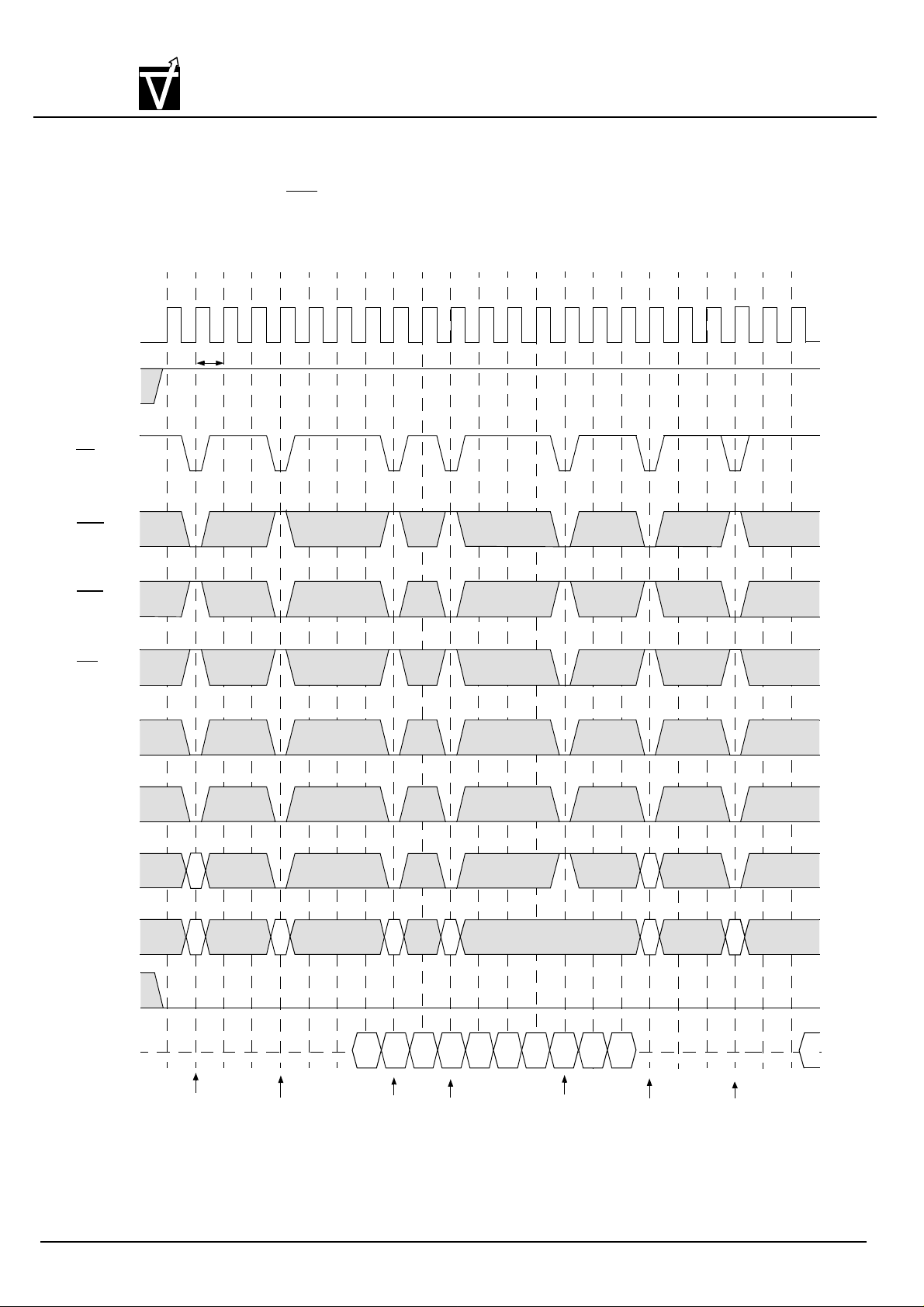
VG4616321B/VG4616322B
262,144x32x2-Bit
VIS
Figure 9.3 Random Column Read (Page within same Bank)
(Burst Length = 4, CAS Latency = 3)
Preliminary CMOS Synchronous Graphic RAM
T0 T1 T2 T3 T4 T5 T6 T7 T8 T9 T10 T11 T12 T13 T14 T15 T16 T17 T18 T19 T20 T21 T22
T0 T1 T2 T3 T4 T5 T6 T7 T8 T9 T10 T11 T12 T13 T14 T15 T16 T17 T18 T19 T20 T21 T22
CLK
CKE
CS
RAS
CAS
WE
DSF
t
CK3
BS
A9
A0 ~ A8
RAw
RAw
CAw
CAx
CAy
RAz
RAz
CAz
DQM
DQ
Note: CKE to CLK disable/enable = 1 clock
Hi-Z
Activate
Command
Bank A
Read
Command
Bank A
Aw1 Aw2 Aw3
Read
Command
Bank A
Read
Command
Bank A
Ax0
Ax1
Ay0 Ay1Aw0
Precharge
Command
Bank A
Ay2
Ay3
Activate
Command
Bank A
Read
Command
Bank A
Document:1G5-0145 Rev.1 Page 41
Az0
Page 42
VIS
VG4616321B/VG4616322B
262,144x32x2-Bit
Preliminary CMOS Synchronous Graphic RAM
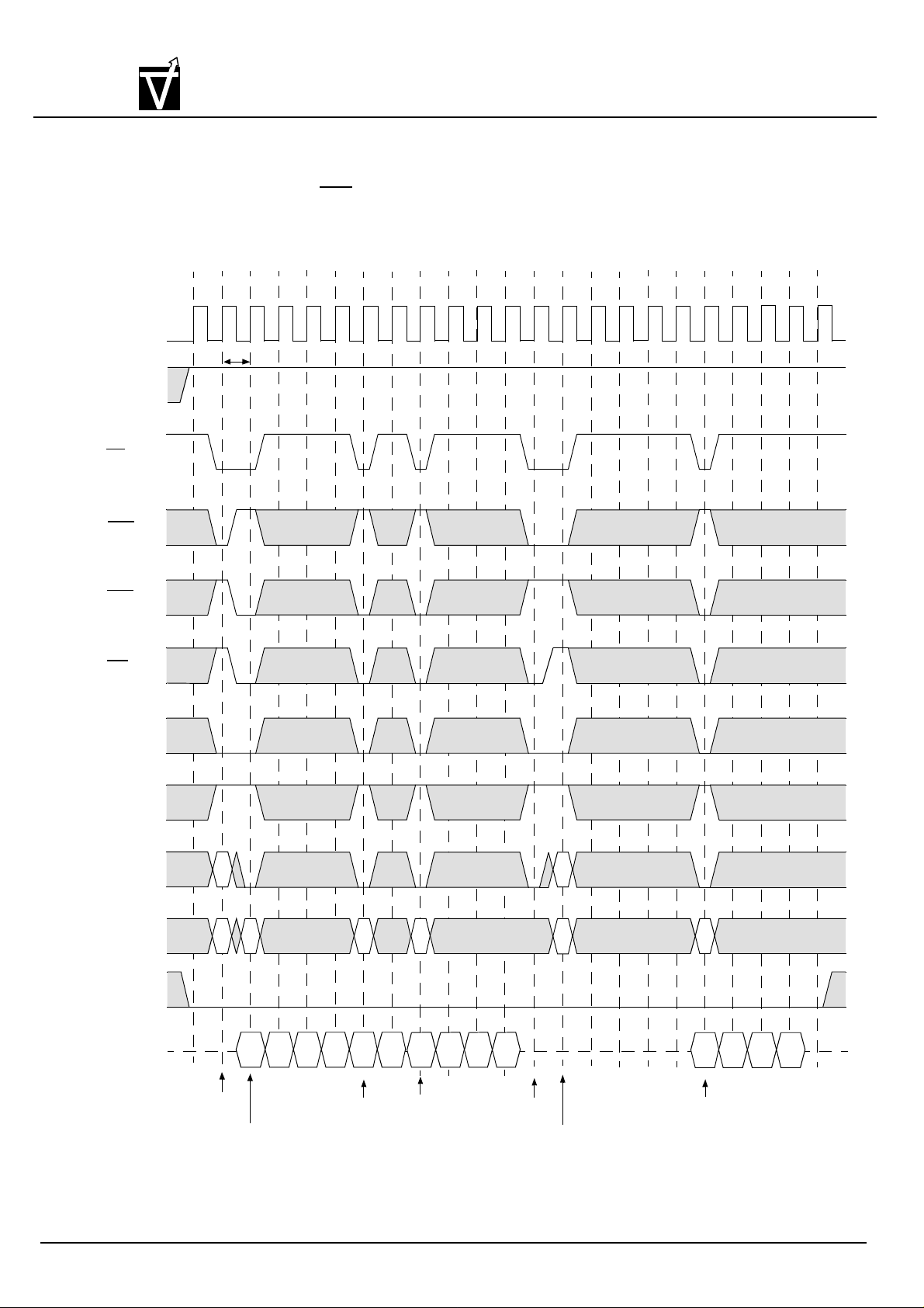
Figure 10.1
Random Column Write (Page within same Bank)
(Burst Length = 4, CAS Latency = 1)
T0 T1 T2 T3 T4 T5 T6 T7 T8 T9 T10 T11 T12 T13 T14 T15 T16 T17 T18 T19 T20 T21 T22
CLK
CKE
CS
RAS
CAS
t
CK1
WE
DSF
BS
A9
A0 ~ A8
DQM
DQ
Hi-Z
RBw
RBw
Activate
Command
Bank B
Command
Bank B
CBw
DBw0
Write
DBw1 DBw2
DBw3
Command
CBx
DBx0
Write
Bank B
CBy
DBx1 DBy0
Write
Command
Bank B
DBy1
RBz
RBz CBz
DBy2
DBy3 DBz0
Precharge
Command
Bank B
Activate
Command
Bank B
Write
Command
Bank B
DBz1
DBz2 DBz3
Document:1G5-0145 Rev.1 Page 42
Page 43
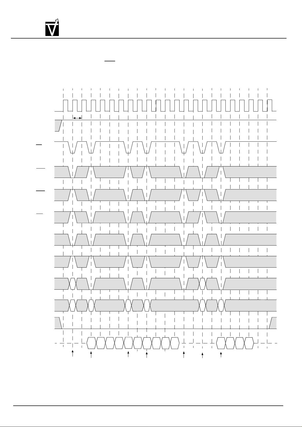
VIS
VG4616321B/VG4616322B
262,144x32x2-Bit
Preliminary CMOS Synchronous Graphic RAM
Figure 10.2
Random Column Write (Page within same Bank)
(Burst Length = 4, CAS Latency = 2)
T0 T1 T2 T3 T4 T5 T6 T7 T8 T9 T10 T11 T12 T13 T14 T15 T16 T17 T18 T19 T20 T21 T22
CLK
CKE
CS
RAS
CAS
t
CK2
WE
DSF
BS
A9
A0 ~ A8
DQM
DQ
RBw
RBw CBy CBx CBy
Hi-Z
Activate
Command
Bank B
DBw1 DBw2
DBw0
Write
Command
Bank B
DBw3
Command
DBx0
Write
Bank B
DBx1 DBy0
Write
Command
Bank B
DBy1
DBy2
DBy3
Precharge
Command
Bank B
RBz
RBz
Activate
Command
Bank B
CBz
DBz0
Write
Command
Bank B
DBz1 DBz2 DBz3
Document:1G5-0145 Rev.1 Page 43
Page 44
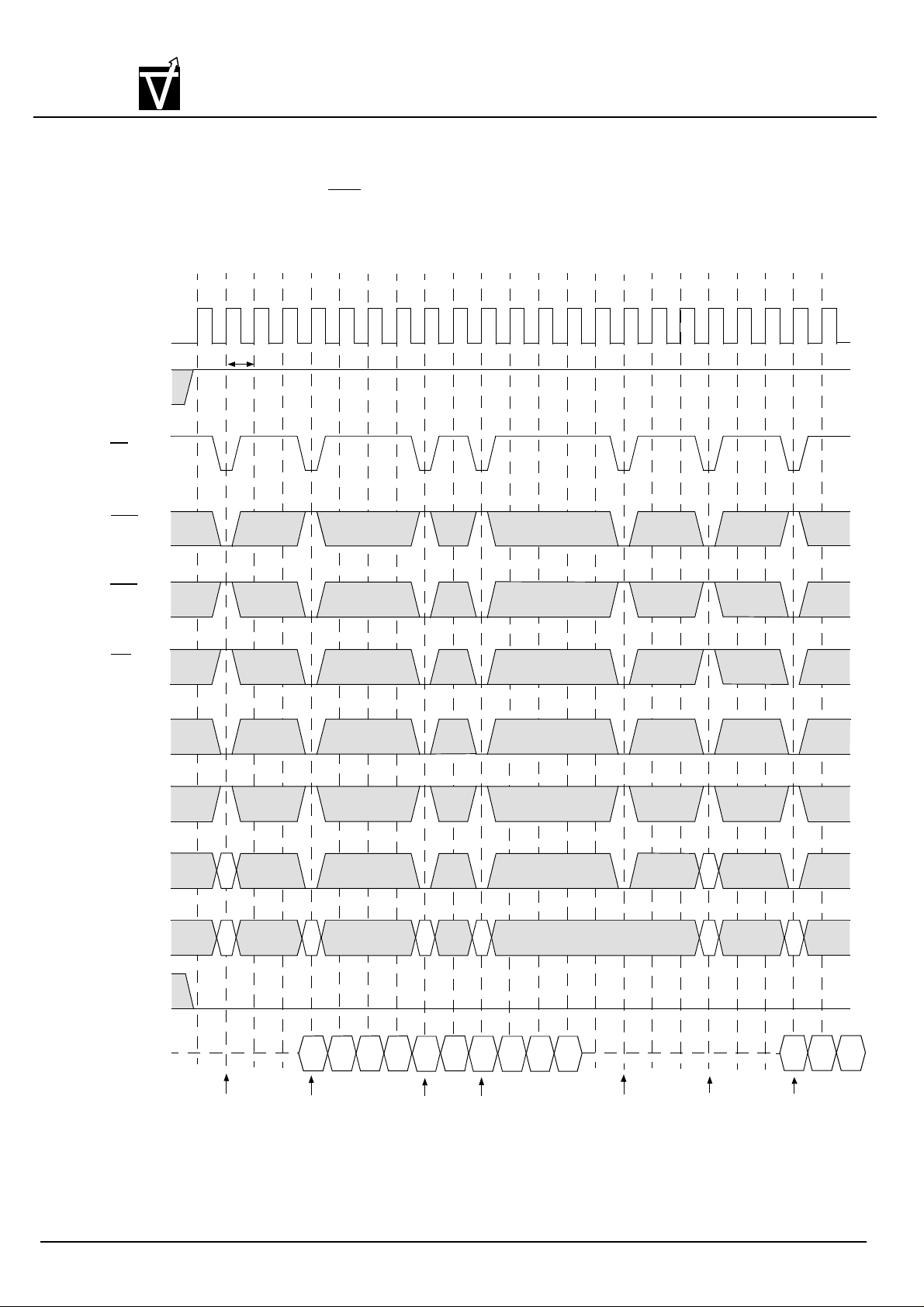
VIS
VG4616321B/VG4616322B
262,144x32x2-Bit
Preliminary CMOS Synchronous Graphic RAM
Figure 10.3
Random Column Write (Page within same Bank)
(Burst Length = 4, CAS Latency = 3)
T0 T1 T2 T3 T4 T5 T6 T7 T8 T9 T10 T11 T12 T13 T14 T15 T16 T17 T18 T19 T20 T21 T22
CLK
CKE
CS
RAS
CAS
t
CK3
WE
DSF
BS
A9
A0 ~ A8
DQM
DQ
Hi-Z
RBw
RBw
Activate
Command
Bank B
CBw
DBw0
Write
Command
Bank B
DBw1 DBw2
DBw3
Command
Bank B
CBx
DBx0
Write
DBx1
Command
Bank B
CBy
DBy0
Write
DBy1
RBz
RBz
DBy2
DBy3 DBz0
Precharge
Command
Bank B
Activate
Command
Bank B
CBz
Write
Command
Bank B
DBz1 DBz2
Document:1G5-0145 Rev.1 Page 44
Page 45
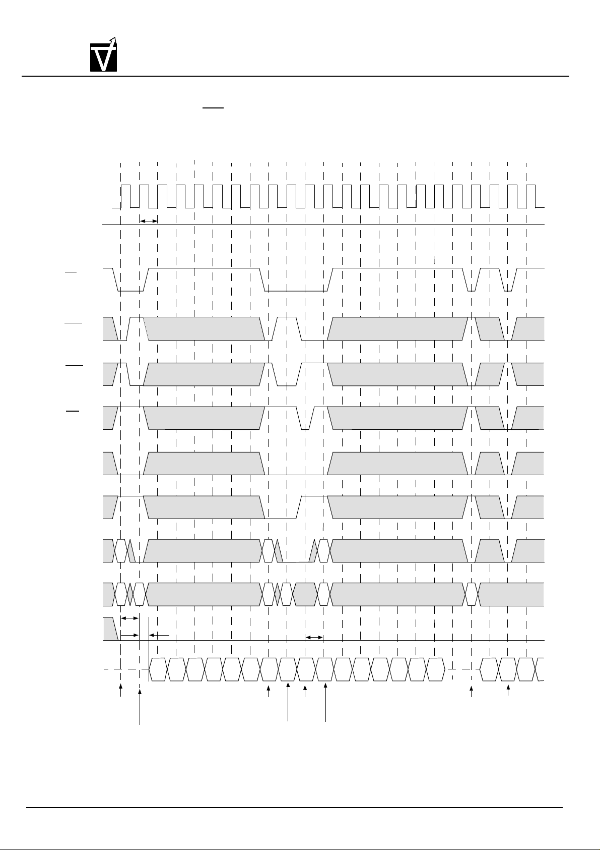
VIS
VG4616321B/VG4616322B
262,144x32x2-Bit
Preliminary CMOS Synchronous Graphic RAM
Figure 11.1
Random Row Read (Interleaving Banks)
(Burst Length = 8, CAS Latency = 2)
T0 T1 T2 T3 T4 T5 T6 T7 T8 T9 T10 T11 T12 T13 T14 T15 T16 T17 T18 T19 T20 T21 T22
CLK
t
CK1
CKE
CS
RAS
CAS
High
WE
DSF
BS
A9
A0 ~ A8
DQM
DQ
RBx
RBx CBx
t
RCD
Hi-Z
Activate
Command
Bank B
Command
Read
Bank B
t
AC1
Bx0
Bx1
Bx2
Bx3
Bx4
Bx5
Activate
Command
Bank A
RBx
RAx
Bx6
CAx
Bx7 Ax0
Precharge
Command
Bank B
Read
Command
Bank A
RBy
RBy
t
RP
Ax1
Activate
Command
Bank B
Ax2
Ax3
Ax4
Ax5 Ax6
Ax7
CBy
By0 By1
Read
Command
Bank B
Precharge
Command
Bank A
By2
Document:1G5-0145 Rev.1 Page 45
Page 46
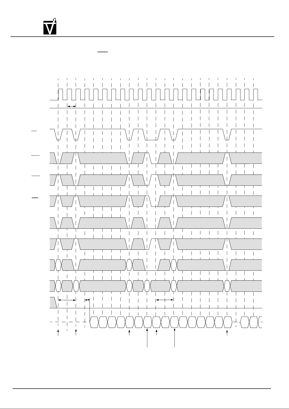
VIS
VG4616321B/VG4616322B
262,144x32x2-Bit
Preliminary CMOS Synchronous Graphic RAM
Figure 11.2
Random Row Read (lnterleaving Banks)
(Burst Length = 8, CAS Latency = 2)
T0 T1 T2 T3 T4 T5 T6 T7 T8 T9 T10 T11 T12 T13 T14 T15 T16 T17 T18 T19 T20 T21 T22
CLK
CKE
CS
RAS
CAS
High
t
CK2
WE
DSF
BS
A9
A0 ~ A8
DQM
DQ
RBx
RBx
Hi-Z
Activate
Command
Bank B
t
RCD
Read
Command
Bank B
CBx
t
AC2
Bx0
Bx1 Bx2
RBx
RAx
Bx3 Bx4
Activate
Command
Bank A
CAx
Bx5 Bx6
Read
Command
Bank A
Bx7
Precharge
Command
Bank B
t
RP
Ax0
Activate
Command
Bank B
RBy
RBy
Ax1
Ax2
Ax3
Ax4
Ax5
Ax6
CBy
Ax7
Read
Command
Bank B
By0
By1
Document:1G5-0145 Rev.1 Page 46
Page 47

VIS
VG4616321B/VG4616322B
262,144x32x2-Bit
Preliminary CMOS Synchronous Graphic RAM
Figure 11.3
Random Row Read (Interleaving Banks)
(Burst Length = 8, CAS Latency = 3)
T0 T1 T2 T3 T4 T5 T6 T7 T8 T9 T10 T11 T12 T13 T14 T15 T16 T17 T18 T19 T20 T21 T22
CLK
CKE
CS
RAS
CAS
High
t
CK3
WE
DSF
BS
A9
A0 ~ A8
DQM
DQ
RBx
RBx
Hi-Z
Activate
Command
Bank B
CBx CAx
t
RCD
Read
Command
Bank B
t
AC3
Bx0
Bx1
Activate
Command
Bank A
Bx2
RAx
RAx
Bx3
Bx4
Read
Command
Bank A
Bx5
Bx6
Precharge
Command
Bank B
Bx7
Ax0
t
RP
Ax1 Ax2
RBy
RBy
Activate
Command
Bank B
Ax3 Ax4
CBy
Ax5
Ax6 By0
Read
Command
Bank B
Ax7
Precharge
Command
Bank A
Document:1G5-0145 Rev.1 Page 47
Page 48

VIS
VG4616321B/VG4616322B
262,144x32x2-Bit
Preliminary CMOS Synchronous Graphic RAM
Figure 12.1
Random Row Read (Interleaving Banks)
(Burst Length = 8, CAS Latency = 1)
T0 T1 T2 T3 T4 T5 T6 T7 T8 T9 T10 T11 T12 T13 T14 T15 T16 T17 T18 T19 T20 T21 T22
CLK
CKE
CS
RAS
CAS
High
t
CK1
WE
DSF
BS
A9
A0 ~ A8
DQM
DQ
RAx
RAx
t
Hi-Z
Activate
Command
Bank A
CAx
RCD
DAx0
Write
Command
Bank A
DAx1
DAx2
DAx3
DAx4
DAx5DAx6
RBx
RBx
DAx7
Activate
Command
Bank B
Command
CBx
DBx0
Write
Bank B
DBx1
DBx2DBx3
DBx4
Precharge
Command
Bank A
RAy
RAy
t
RP
DBx5
Activate
Command
Bank A
DBx6
DBx7
t
WR
Precharge
Command
Bank B
CAy
DAy0
Write
Command
Bank A
DAy1
DAy2
DAy3
Document:1G5-0145 Rev.1 Page 48
Page 49
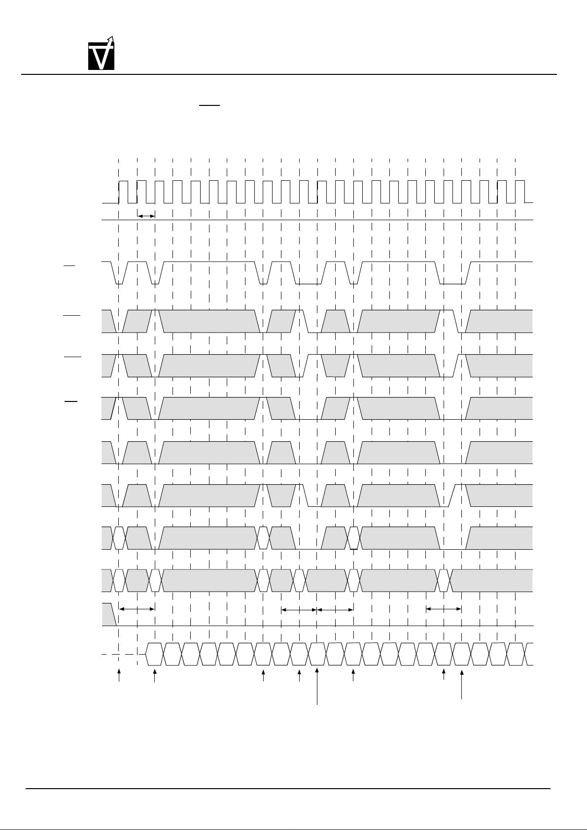
VIS
VG4616321B/VG4616322B
262,144x32x2-Bit
Preliminary CMOS Synchronous Graphic RAM
Figure 12.2
Random Row Write (Interleaving Banks)
(Brust Length = 4, CAS Latency = 2)
T0 T1 T2 T3 T4 T5 T6 T7 T8 T9 T10 T11 T12 T13 T14 T15 T16 T17 T18 T19 T20 T21 T22
CLK
CKE
CS
RAS
CAS
High
t
CK2
WE
DSF
BS
A9
A0 ~ A8
DQM
DQ
* t
Hi-Z
Command
WR > tWR(min.)
RAx
RAx
Activate
Bank A
CAx CBx
t
RCD
DAx0
Write
Command
Bank A
DAx1
DAx2
DAx3
DAx4
DAx5 DAx6
Activate
Command
Bank B
RBx
RBx
DAx7 DBx0 DBx1
Command
t
Write
Bank B
WR*
Precharge
Command
Bank A
t
RP
DBx2
RAy
RAy
DBx3
Activate
Command
Bank A
DBx4
DBx5 DBx6
DBx7
CAy
t
WR*
DAy0
Write
Command
Bank A
Precharge
Command
DAy1
Bank B
DAy2
DAy3
DAy4
Document:1G5-0145 Rev.1 Page 49
Page 50
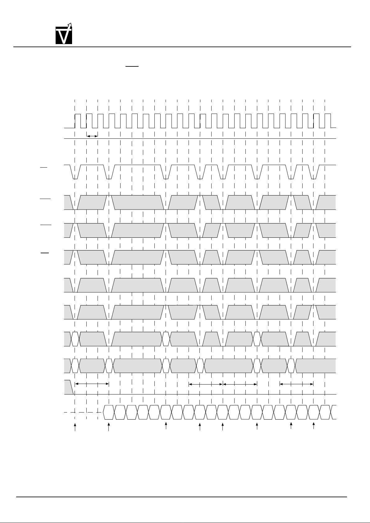
VIS
VG4616321B/VG4616322B
262,144x32x2-Bit
Preliminary CMOS Synchronous Graphic RAM
Figure 12.3
Random Row Write (Interleaving Banks)
(Burst Length = 8, CAS Latency = 3)
T0 T1 T2 T3 T4 T5 T6 T7 T8 T9 T10 T11 T12 T13 T14 T15 T16 T17 T18 T19 T20 T21 T22
CLK
CKE
CS
RAS
CAS
High
t
CK3
WE
BS
BS
A9
A0 ~ A8
DQM
DQ
RBx
RBx
Hi-Z
Activate
Command
Bank A
t
RCD
CAx
DAx0
Write
Command
Bank A
DAx1 DAx2 DAx3
DAx4
RBx
RBx
DAx5
Activate
Command
Bank B
DAx6
DAx7
CBx
tWR*
DBx0
Write
Command
Bank B
DBx1
DBx2
Precharge
Command
Bank A
t
RP
DBx3
DBx4 DBx5 DBx6
RAy
RAy
Activate
Command
Bank A
DBx7
CAy
DAy0
Write
Command
Bank A
R*tW
DAy1 DAy2 DAy3
Precharge
Command
Bank B
*t
> tWR (min)
WR
Document:1G5-0145 Rev.1 Page 50
Page 51

VIS
VG4616321B/VG4616322B
262,144x32x2-Bit
Preliminary CMOS Synchronous Graphic RAM
Figure 13.1
CLK
CKE
CS
RAS
CAS
Read and Write Cycle (Burst Length = 4, CAS Latency = 1)
T0 T1 T2 T3 T4 T5 T6 T7 T8 T9 T10 T11 T12 T13 T14 T15 T16 T17 T18 T19 T20 T21 T22
t
CK1
WE
DSF
BS
A9
A0 ~ A8
DQM
DQ
Hi-Z
Activate
Command
Bank A
RAx
CAx CAy
RAx
Ax0 Ax1 Ax2 Ax3
Read
Command
Bank A
DAy1 Az0
DAy0
Write
Command
Bank A
The Write Data
is Masked with a
Zero Clock
Latency
DAy3
CAz
Read
Command
Bank A
Az1 Az3
The Read Data
is Masked with a
Two Clock
Latency
Document:1G5-0145 Rev.1 Page 51
Page 52

VIS
VG4616321B/VG4616322B
262,144x32x2-Bit
Preliminary CMOS Synchronous Graphic RAM
Figure 13.2
CLK
CKE
CS
RAS
CAS
Read and Write Cycle (Burst Length = 4, CAS Latency = 2)
T0 T1 T2 T3 T4 T5 T6 T7 T8 T9 T10 T11 T12 T13 T14 T15 T16 T17 T18 T19 T20 T21 T22
t
CK2
WE
DSF
BS
A9
A0 ~ A8
DQM
DQ
Hi-Z
RAx
RAx CAx
Activate
Command
Bank A
Read
Command
Bank A
Ax0
Ax1 Ax2 Ax3
CAy
DAy0
Write
Command
Bank A
DAy1
The Write Data
is Masked with a
Zero Clock
Latency
DAy3
CAz
Read
Command
Bank A
Az0 Az1
Az3
The Read Data
is Masked with a
Two Clock
Latency
Document:1G5-0145 Rev.1 Page 52
Page 53
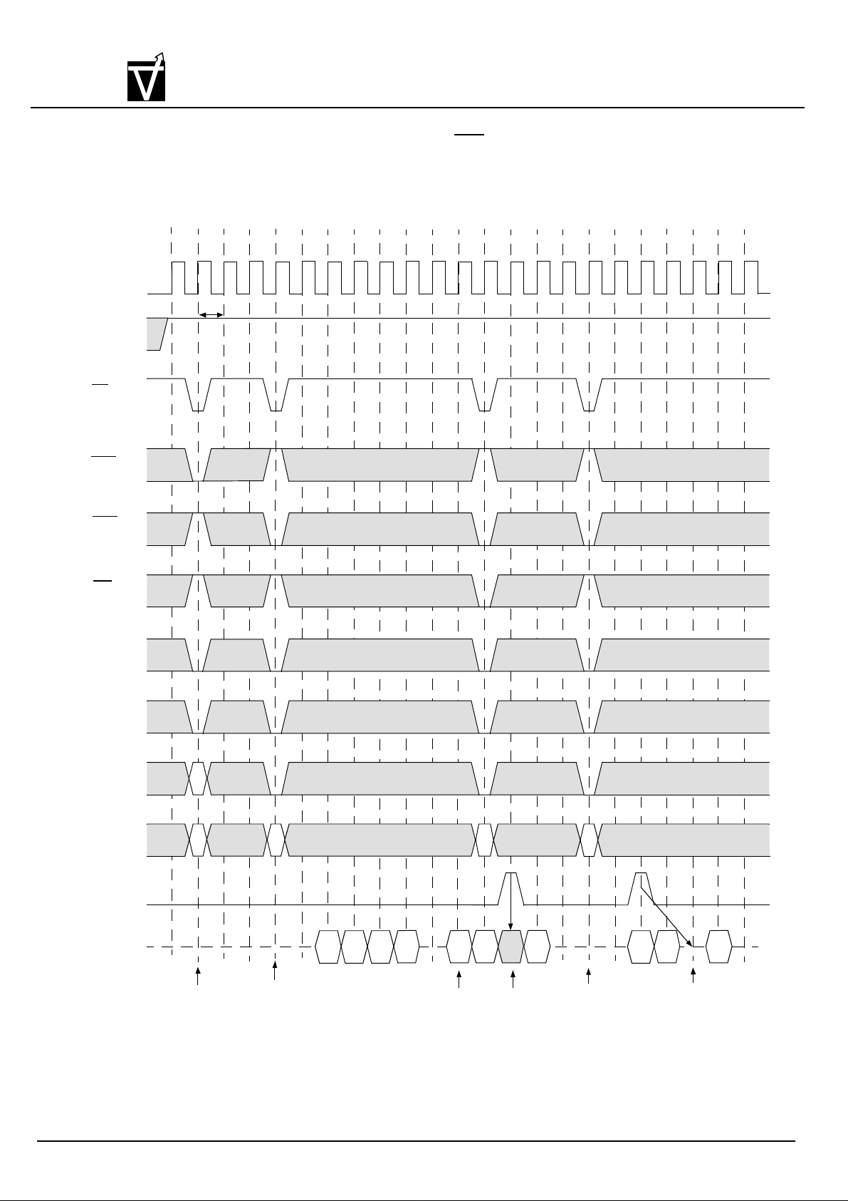
VIS
Figure 13.3 Read and Write Cycle (Burst Length = 4, CAS Latency = 3)
VG4616321B/VG4616322B
262,144x32x2-Bit
Preliminary CMOS Synchronous Graphic RAM
T0 T1 T2 T3 T4 T5 T6 T7 T8 T9 T10 T11 T12 T13 T14 T15 T16 T17 T18 T19 T20 T21 T22
CLK
CKE
CS
RAS
CAS
WE
DSF
t
CK3
BS
A9
A0 ~ A8
DQM
DQ
Hi-Z
RAx
RAx
Activate
Command
Bank A
CAx
Read
Command
Bank A
Ax0
Ax1 Ax2 Ax3
DAy0
Write
Command
Bank A
CAy
DAy1
The Write Data
is Masked with a
Zero Clock
Latency
DAy3
CAz
Read
Command
Bank A
Az0 Az1
Az3
The Read Data
is Masked with a
Two Clock
Latency
Document:1G5-0145 Rev.1 Page 53
Page 54
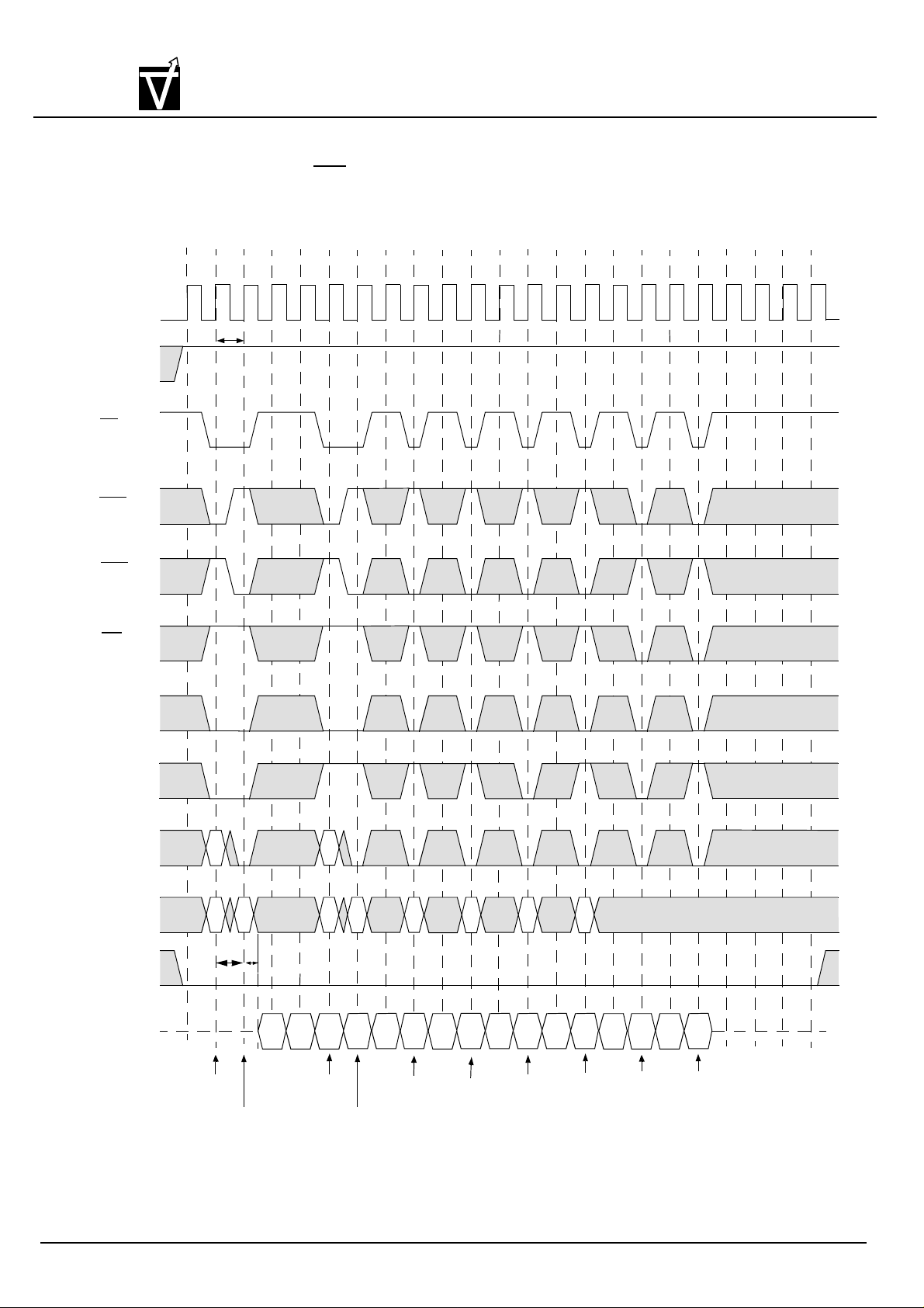
VIS
VG4616321B/VG4616322B
262,144x32x2-Bit
Preliminary CMOS Synchronous Graphic RAM
Figure 14.1
Interleaving Column Read Cycle
(Burst Length = 4, CAS Latency = 1)
T0 T1 T2 T3 T4 T5 T6 T7 T8 T9 T10 T11 T12 T13 T14 T15 T16 T17 T18 T19 T20 T21 T22
CLK
CKE
CS
RAS
CAS
t
CK1
WE
DSF
BS
A9
A0 ~ A8
DQM
DQ
Hi-Z
RAx
RAx CAx
t
RCD
Activate
Command
Bank A
Command
Read
Bank A
t
AC1
Ax0
Ax1 Ax2 Ax3 Bw0
Activate
Command
Bank B
RBw
RBw CBw
Read
Command
Bank B
CBx CBy CBz
Bx0 Bx1
Read
Command
Bank B
Read
Command
Bank B
By0
CAy
By1
Read
Command
Bank A
Ay0
Ay1
Read
Command
Bank B
Bz0
Precharge
Command
Bz1
Bz1Bw1
Bank A
Bz2
Precharge
Command
Bz3
Bank B
Document:1G5-0145 Rev.1 Page 54
Page 55
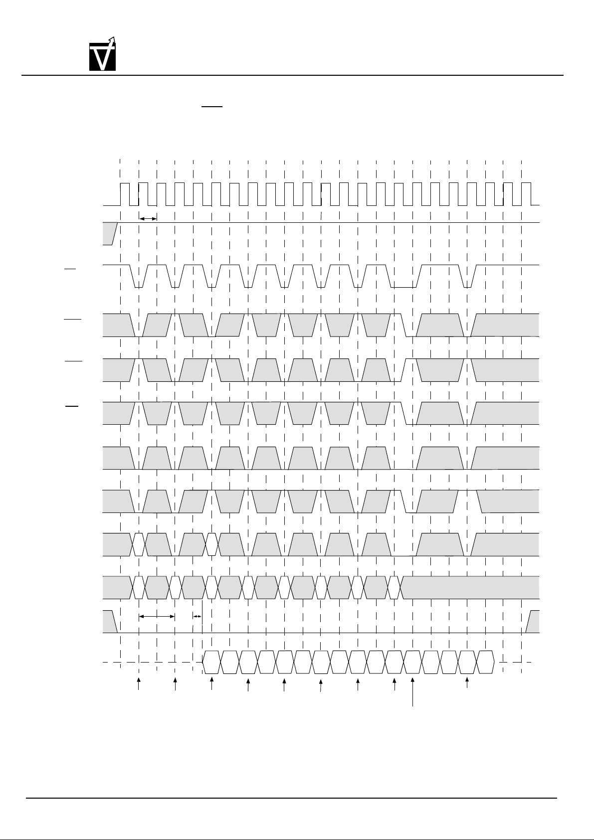
VIS
VG4616321B/VG4616322B
262,144x32x2-Bit
Preliminary CMOS Synchronous Graphic RAM
Figure 14.2
Interleaving Column Read Cycle
(Burst Length = 4, CAS Latency = 2)
T0 T1 T2 T3 T4 T5 T6 T7 T8 T9 T10 T11 T12 T13 T14 T15 T16 T17 T18 T19 T20 T21 T22
CLK
CKE
CS
RAS
CAS
t
CK2
WE
DSF
BS
A9
A0 ~ A8
DQM
DQ
Hi-Z
RAx
RAx
Activate
Command
Bank A
t
RCD
CAx
Read
Command
Bank A
RBw
RBw
t
AC2
Ax0
Activate
Command
Bank B
CBw CBx CAyCBy
Ax1 Ax2 Ax3 Bw0
Read
Command
Bank B
Read
Command
Bank B
Bw1
Command
Bx0 Bx1
Read
Bank B
By0
Read
Command
Bank A
By1
Command
CBz
Ay0
Read
Bank B
Ay1
Precharge
Command
Bank A
Bz0
Bz1
Precharge
Command
Bz2
Bank B
Bz3
Document:1G5-0145 Rev.1 Page 55
Page 56
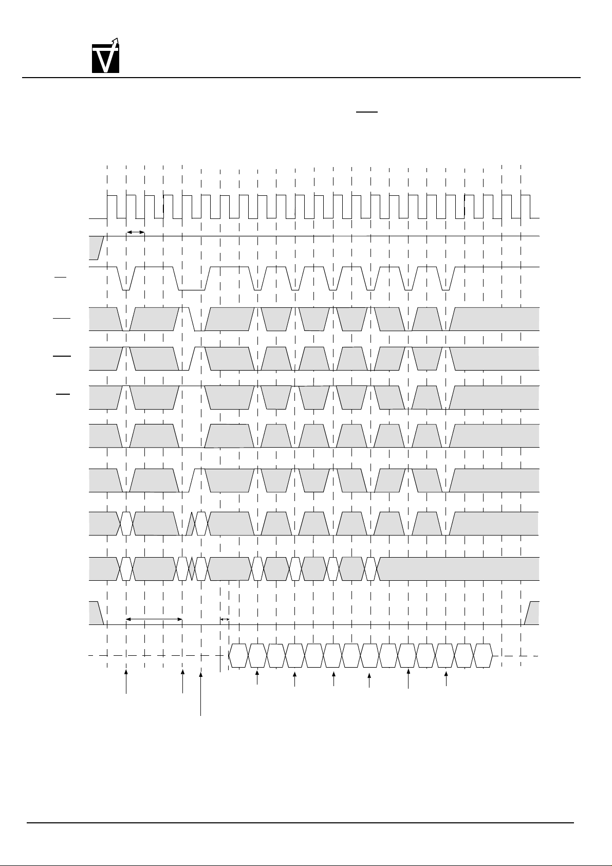
VG4616321B/VG4616322B
262,144x32x2-Bit
VIS
Figure 14.3. Interleaved Column Read Cycle (Burst Length = 4, CAS Latency = 3)
CLK
CKE
CS
RAS
Preliminary CMOS Synchronous Graphic RAM
T0 T1 T2 T3 T4 T5 T6 T7 T8 T9 T10 T11 T12 T13 T14 T15 T16 T17 T18 T19 T20 T21 T22
t
CK3
CAS
WE
DSF
BS
A9
A0 ~ A8
DQM
DQ
Hi-Z
RAx
RAx
t
RCD
RBx
CAx RBx
CBx CBy CBz CAy
t
AC3
Ax0 Ax1 Ax2 Ax3
Bx0 Bx1
By0
Bz0 Bz1 Ay0 Ay1
By1
Ay2
Ay3
Activate
Command
Bank A
Read
Command
Bank A
Command
Activate
Bank B
Read
Command
Bank B
Read
Command
Bank B
Read
Command
Bank B
Command
Bank A
Read
Precharge
Command
Bank B
Precharge
Command
Bank A
Document:1G5-0145 Rev.1 Page 56
Page 57

VIS
Figure 15.1. Interleaved Column Write Cycle (Burst Length = 4, CAS Latency = 1)
CLK
CKE
CS
RAS
VG4616321B/VG4616322B
262,144x32x2-Bit
Preliminary CMOS Synchronous Graphic RAM
T0 T1 T2 T3 T4 T5 T6 T7 T8 T9 T10 T11 T12 T13 T14 T15 T16 T17 T18 T19 T20 T21 T22
t
CK1
CAS
WE
DSF
BS
A9
A0 ~ A8
DQM
DQ
Hi-Z
RAx
RAx
t
RCD
CAx
t
RRD
DAx0
RBw
RBw
DAx1
DAx2
DAx3
CBw
DBw0
DBw1
CBx
DBx0
DBx1
CBy
DBy0
DBy1
CAy
DAy0
DAy1
CBz
t
RP
DBz1
DBz2
DBz0 DBz3
tWRt
RP
Activate
Command
Bank A
Command
Write
Command
Bank A
Activate
Bank B
Write
Command
Bank B
Write
Command
Bank B
Write
Command
Bank B
Write
Command
Bank A
Command
Precharge
Command
Bank A
Write
Bank B
Precharge
Command
Bank B
Document:1G5-0145 Rev.1 Page 57
Page 58
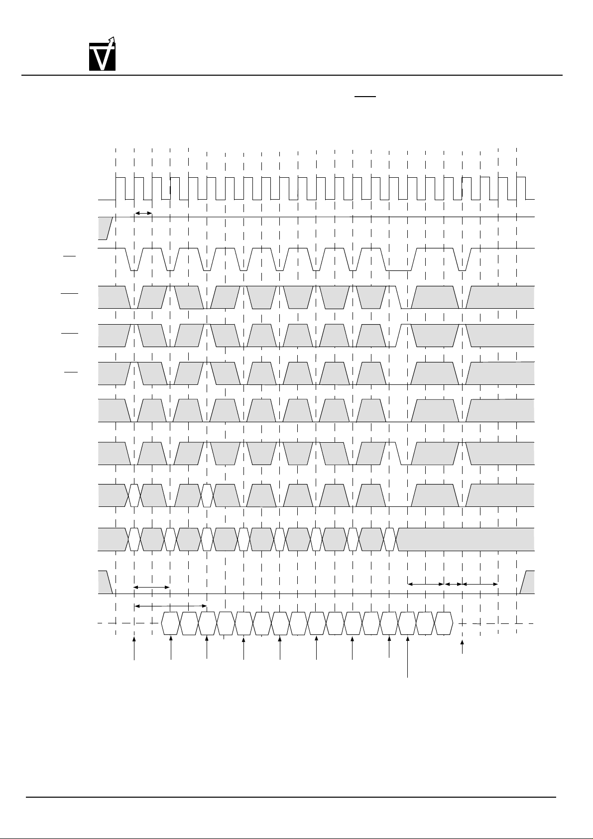
VIS
Figure 15.2. Interleaved Column Write Cycle (Burst Length = 4, CAS Latency = 2)
VG4616321B/VG4616322B
262,144x32x2-Bit
Preliminary CMOS Synchronous Graphic RAM
T0 T1 T2 T3 T4 T5 T6 T7 T8 T9 T10 T11 T12 T13 T14 T15 T16 T17 T18 T19 T20 T21 T22
CLK
CKE
CS
RAS
CAS
WE
DSF
BS
t
CK2
A9
A0 ~ A8
DQM
DQ
Hi-Z
RAx
Activate
Command
Bank A
t
RCD
CAxRAx
t
RRD
DAx0
Write
Command
Bank A
DAx1
Activate
Command
RBw
RBw
DAx2
Bank B
DAx3
Command
DBw0
Write
Bank B
DBw1
Command
DBx0
Write
Bank B
DBx1
Command
CBy
DBy0
Write
Bank B
DBy1
Command
CAyCBxCBw
DAy0
Write
Bank A
CBz
DBz0 DBz3
DAy1
Write
Command
Bank B
Precharge
Command
DBz1
Bank A
t
DBz2
t
t
WR
RP
Command
RP
Precharge
Bank B
Document:1G5-0145 Rev.1 Page 58
Page 59
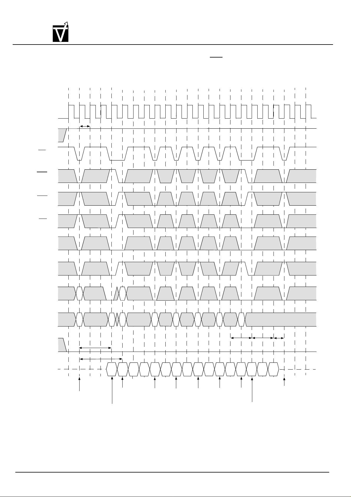
VIS
Figure 15.3. Interleaved Column Write Cycle (Burst Length = 4, CAS Latency = 3)
CLK
CKE
CS
RAS
VG4616321B/VG4616322B
262,144x32x2-Bit
Preliminary CMOS Synchronous Graphic RAM
T0 T1 T2 T3 T4 T5 T6 T7 T8 T9 T10 T11 T12 T13 T14 T15 T16 T17 T18 T19 T20 T21 T22
t
CK3
CAS
WE
DSF
BS
A9
A0 ~ A8
DQM
DQ
Hi-Z
RAx
t
RRD
t
RCD
> t
CAxRAx
RRD(min)
DAx0
RBw
RBw
DAx1
DAx2
DAx3
DBw0
DBw1
DBx0
DBx1
CBy
DBy0
DBy1
CAyCBxCBw
DAy0
CBz
t
WR
DBz0 DBz3
DAy1
DBz1
t
RP
DBz2
t
WR (min)
Activate
Command
Bank A
Command
Write
Command
Bank A
Activate
Bank B
Write
Command
Bank B
Write
Command
Bank B
Write
Command
Bank B
Write
Command
Bank A
Write
Command
Bank B
Precharge
Command
Bank A
Precharge
Command
Bank B
Document:1G5-0145 Rev.1 Page 59
Page 60
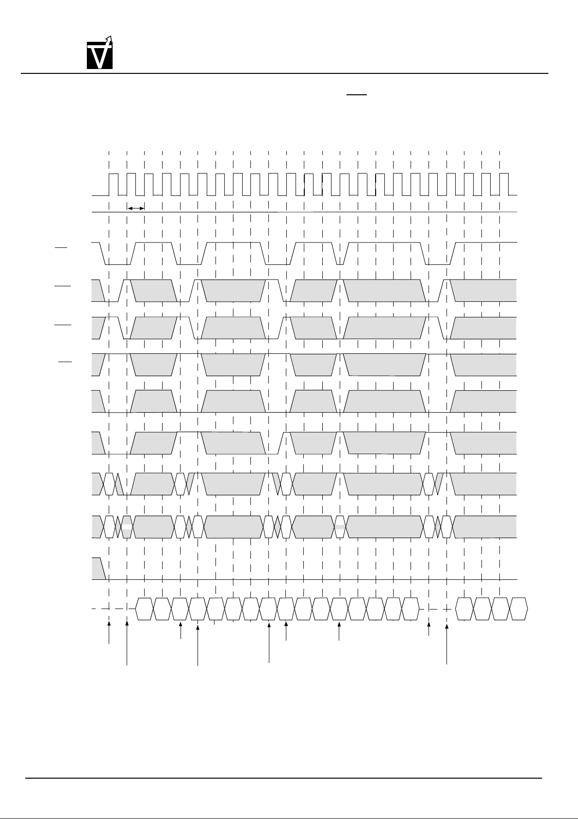
VG4616321B/VG4616322B
262,144x32x2-Bit
VIS
Figure 16.1. Auto Precharge after Read Burst (Burst Length = 4, CAS Latency = 1)
CLK
CKE
CS
RAS
Preliminary CMOS Synchronous Graphic RAM
T0 T1 T2 T3 T4 T5 T6 T7 T8 T9 T10 T11 T12 T13 T14 T15 T16 T17 T18 T19 T20 T21 T22
t
CK1
High
CAS
WE
DSF
BS
A9
A0~A8
DQM
DQ
Hi-Z
RAx
CAx CBy
RBx
CAxRAx RBz
CBx
Ax1 Ax2
Ax3
Bx0
Bx1
Bx2
CAy
Bx3
RBy
RBy
Ay0 Ay1
Ay2
Ay3
By0
RBz
CBz
By2
By1Ax0
By3
Bz0 Bz1
Bz2
Bz3
Activate
Command
Bank A
Command
Read
Bank A
Activate
Command
Bank B
Read with
Auto Precharge
Command
Bank B
Activate
Command
Bank B
Read with
Auto Precharge
Command
Bank A
Read with
Auto Precharge
Command
Bank B
Activate
Command
Bank B
Auto Precharge
Read with
Command
Bank B
Document:1G5-0145 Rev.1 Page 60
Page 61
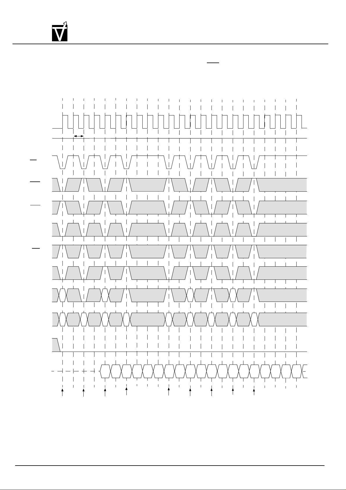
VG4616321B/VG4616322B
262,144x32x2-Bit
VIS
Figure 16.2 Auto Precharge after Read Burst (Burst Length = 4, CAS Latency = 2)
CLK
CKE
CS
RAS
Preliminary CMOS Synchronous Graphic RAM
T0 T1 T2 T3 T4 T5 T6 T7 T8 T9 T10 T11 T12 T13 T14 T15 T16 T17 T18 T19 T20 T21 T22
t
CK2
High
CAS
DSF
WE
BS
A9
A0 ~ A8
DQM
DQ
RAx
RAx RAz
Hi-Z
CAx
RBx
RBx CBx
Ax0
Ax1
Ax2 Ax3
Bx0
Bx1
RAy
Bx2 Bx3
RBy
RBy
Ay0
Ay1
CBy
Ay2
Ay3
RAz
By0
By1
CAz
By2
By3 Az0
Az1
Az2
Activate
Command
Bank A
Read with
Command
Bank A
Activate
Command
Bank B
Read with
Auto Precharge
Command
Bank B
Read with
Auto Precharge
Command
Bank A
Activate
Command
Bank B
Read with
Auto Precharge
Command
Bank B
Activate
Command
Bank A
Read with
Auto Precharge
Command
Bank A
Document:1G5-0145 Rev.1 Page 61
Page 62

VG4616321B/VG4616322B
262,144x32x2-Bit
VIS
Figure 16.3 Auto Precharge after Read Burst (Burst Length = 4, CAS Latency = 3)
CLK
CKE
CS
RAS
High
Preliminary CMOS Synchronous Graphic RAM
T0 T1 T2 T3 T4 T5 T6 T7 T8 T9 T10 T11 T12 T13 T14 T15 T16 T17 T18 T19 T20 T21 T22
t
CK3
CAS
WE
DSF
BS
A9
A0 ~ A8
DQM
RAx RBx RBy
RAx CBx
Hi-Z
CAx
RBx
Ax0
Ax1
Ax2
Ax3
Bx0
CAy
Bx1 Bx2
Bx3
RBy
Ay0
Ay1
Ay2
CBy
Ay3
BY0
BY1
BY2
BY3
Activate
Command
Bank A
Command
Read
Command
Bank A
Activate
Bank B
Read with
Auto Precharge
Command
Bank B
Read with
Auto Precharge
Command
Bank A
Activate
Command
Bank B
Read with
Auto Precharge
Command
Bank B
Document:1G5-0145 Rev.1 Page 62
Page 63
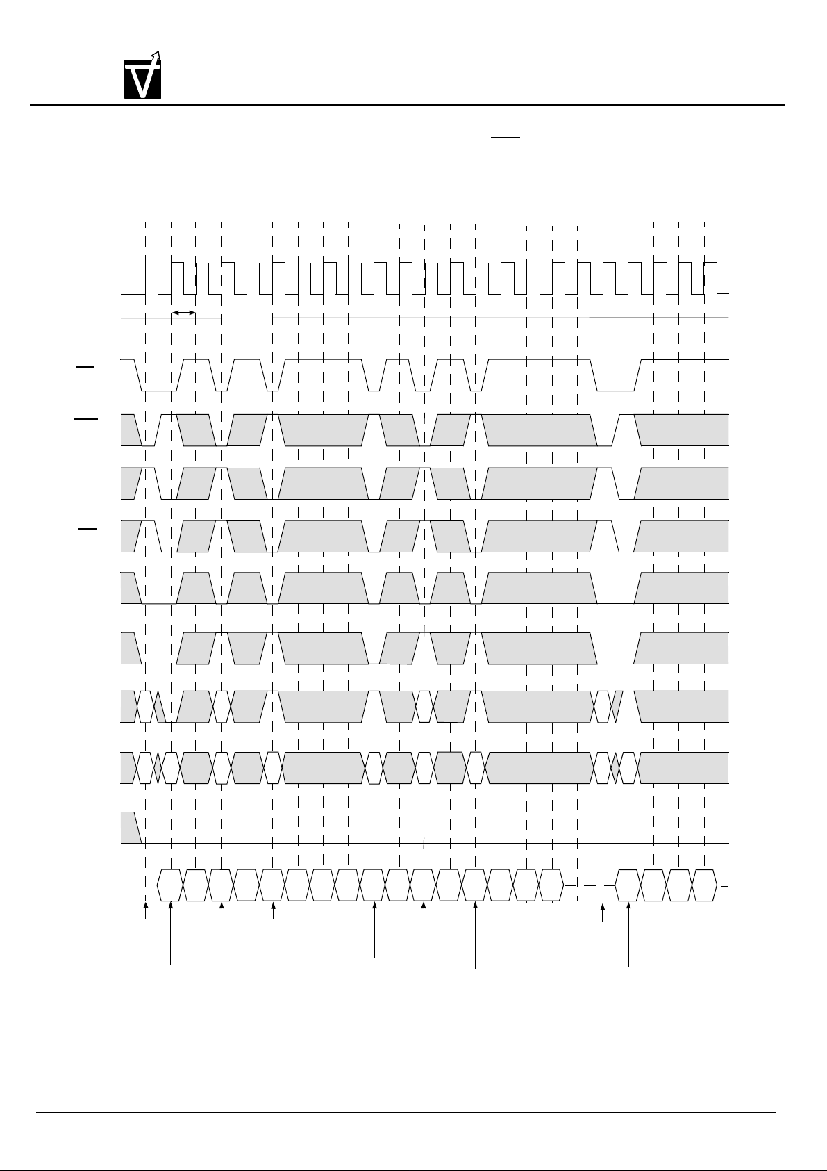
VG4616321B/VG4616322B
262,144x32x2-Bit
VIS
Figure 17.1 Auto Precharge after Write Burst (Burst Length = 4, CAS Latency = 1)
CLK
CKE
CS
RAS
High
Preliminary CMOS Synchronous Graphic RAM
T0 T1 T2 T3 T4 T5 T6 T7 T8 T9 T10 T11 T12 T13 T14 T15 T16 T17 T18 T19 T20 T21 T22
t
CK1
CAS
WE
DSF
BS
A9
A0 ~ A8
DQM
DQ
RAx
RAx
Hi-Z
RBx
CAx
DAx0 DAx1 DAx2
RBx
CBx CAy
DAx3 DBx0
DBx1
DBx2
DBx3
DAy0
RBy
RBy
DAy1 DAy2
CBy
DBy0 DBy1 DBy2
DAy3
DBy3
RAz
RAz
CAz
DAz0
DAz1
DAz2
DAz3
Activate
Command
Bank A
Command
Bank A
Write
Activate
Command
Bank B
Write with
Auto Precharge
Command
Bank B
Write with
Auto Precharge
Command
Bank A
Activate
Command
Bank B
Write with
Auto Precharge
Command
Bank B
Activate
Command
Bank A
Write with
Auto Precharge
Command
Bank A
Document:1G5-0145 Rev.1 Page 63
Page 64
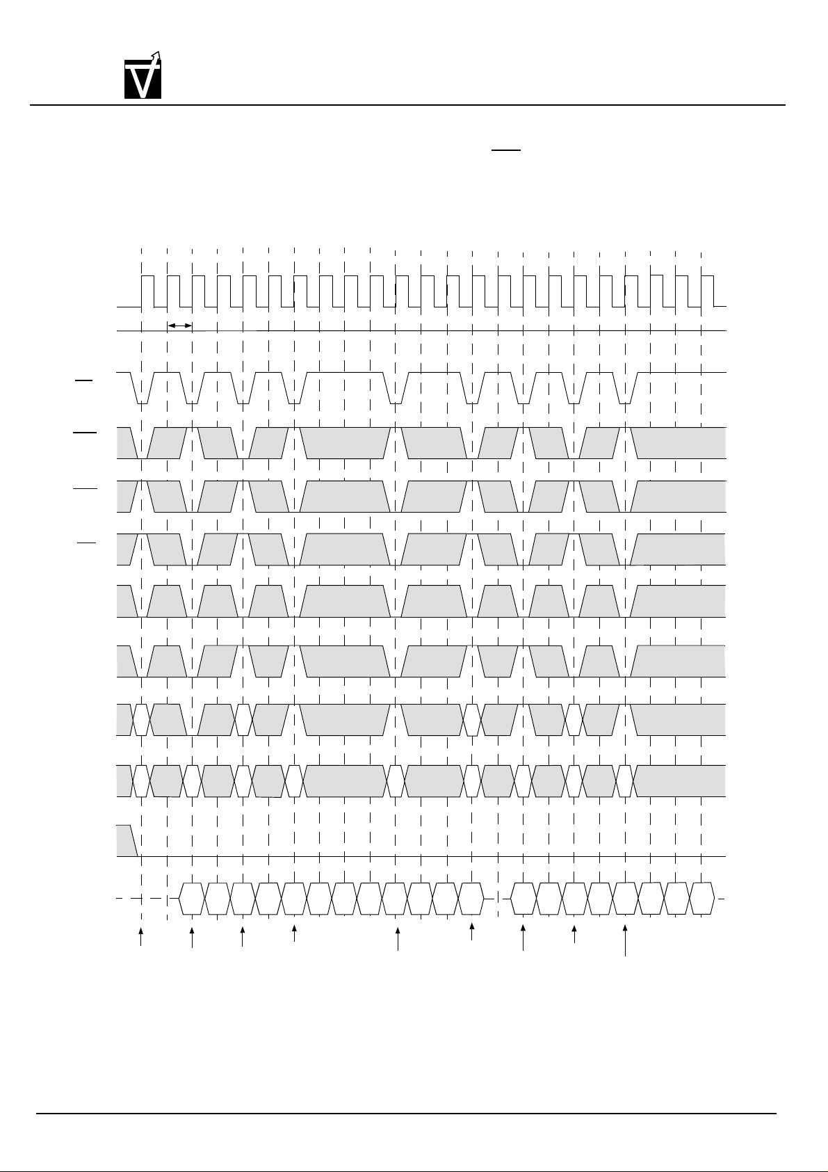
VG4616321B/VG4616322B
262,144x32x2-Bit
VIS
Figure 17.2. Auto Precharge after Write Burst (Burst Length = 4, CAS Latency = 2)
CLK
CKE
CS
RAS
High
Preliminary CMOS Synchronous Graphic RAM
T0 T1 T2 T3 T4 T5 T6 T7 T8 T9 T10 T11 T12 T13 T14 T15 T16 T17 T18 T19 T20 T21 T22
t
CK2
CAS
WE
DSF
BS
A9
A0 ~ A8
DQM
DQ
RAx RBx RBy
RAx
Hi-Z
CAx
DAx0
RBx
DAx1 DAx2
DAx3
CBx
DBx0
DBx1
DBx2 DBx3
CAy
DAy0
DAy1 DAy2
RBy
DAy3
RAz
CBy
DBy0 DBy1 DBy2
RAz
DBy3
CAz
DAz0
DAz1
DAz2
DAz3
Activate
Command
Bank A
Write
Command
Bank A
Activate
Command
Bank B
Write with
Auto Precharge
Command
Bank B
Write with
Auto Precharge
Command
Bank A
Activate
Command
Bank B
Auto Precharge
Command
Bank B
Activate
Command Write with
Bank A
Write with
Auto Precharge
Command
Bank A
Document:1G5-0145 Rev.1 Page 64
Page 65

VG4616321B/VG4616322B
262,144x32x2-Bit
VIS
Figure 17.3. Auto Precharge after Write Burst (Burst Length = 4, CAS Latency = 3)
CLK
CKE
CS
RAS
High
Preliminary CMOS Synchronous Graphic RAM
T0 T1 T2 T3 T4 T5 T6 T7 T8 T9 T10 T11 T12 T13 T14 T15 T16 T17 T18 T19 T20 T21 T22
t
CK3
CAS
WE
DSF
BS
A9
A0 ~ A8
DQM
Hi-Z
RAx
RAx
CAx
DAx0
RBx
RBx
DAx2 DAx3 DBx0
DAx1
CBx
DBx1
DBx2 DBx3 DAy0
CAy
DAy1
DAy2
DAy3
RBy
RBy
CBy
DBy0 DBy1 DBy2
DBy3
Activate
Command
Bank A
Activate
Command
Write
Command
Bank A
Bank B
Write with
Auto Precharge
Command
Bank B
Write with
Auto Precharge
Command
Bank A
Activate
Command
Bank B
Write with
Auto Precharge
Command
Bank B
Document:1G5-0145 Rev.1 Page 65
Page 66
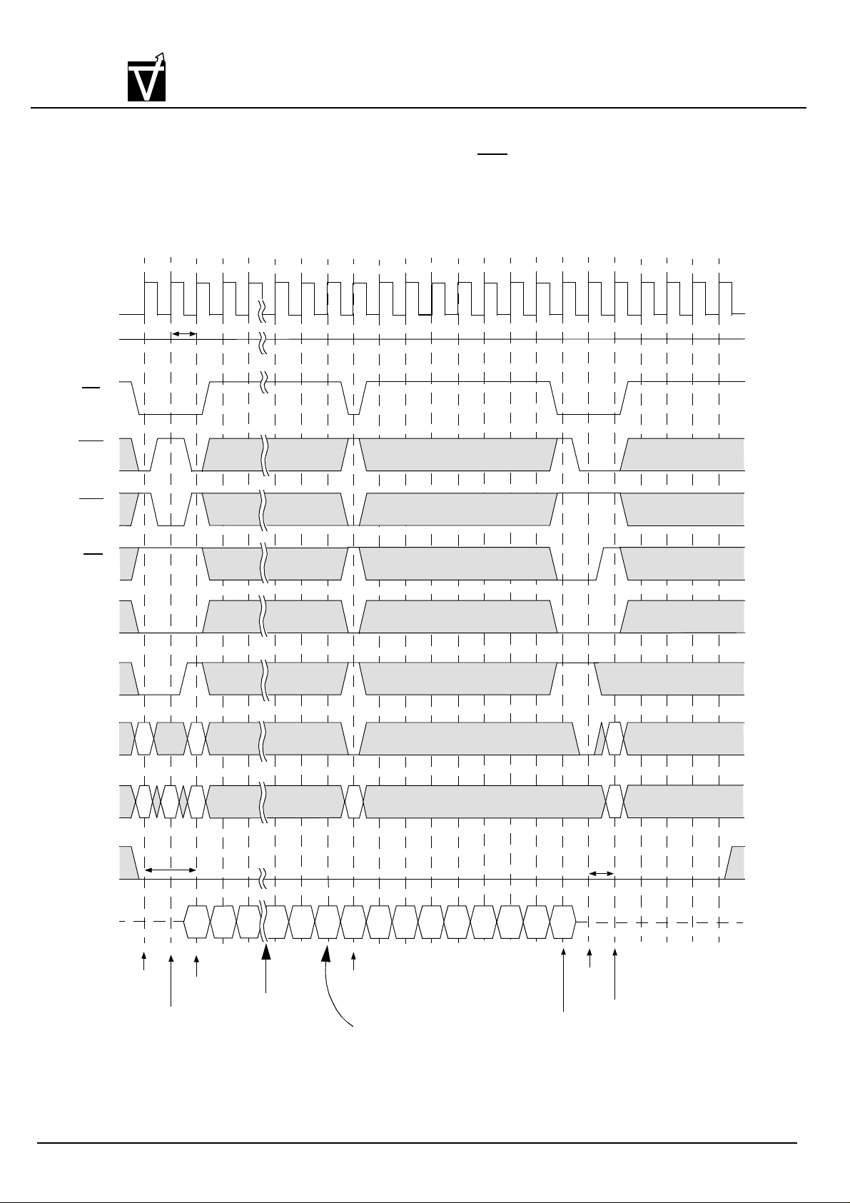
VG4616321B/VG4616322B
262,144x32x2-Bit
VIS
Figure 18.1. Full Page Read Cycle (Burst Length = Full Page, CAS Latency = 1)
CLK
CKE
High
CS
RAS
Preliminary CMOS Synchronous Graphic RAM
T0 T1 T2 T3 T4 T5 T6 T7 T8 T9 T10 T11 T12 T13 T14 T15 T16 T17 T18 T19 T20 T21 T22
t
CK1
CAS
WE
DSF
BS
A9
A0 ~ A8
DQM
DQ
Hi-Z
RAx
RAx
t
CAx
RRD
RBx
RBx
Ax+2 Ax-2 Ax-1
Ax+1
CBx
Ax+1
RBy
RBy
t
RP
Bx
Bx+1
Bx+2
Bx+3
Bx+5 Bx+6 Bx+7Ax
Bx+4Ax
Activate
Command
Bank A
Command
Command
Read
Bank A
Activate
Bank B
The burst counter wraps
from the highest order
page address back to zero
during this time interval
Read
Command
Bank B
Full Page burst operation does not
terminate when the burst length is satisfied;
the burst counter increments and continues
bursting beginning with the starting address.
Precharge
Command
Bank B
Burst Stop
Command
Activate
Command
Bank B
Document:1G5-0145 Rev.1 Page 66
Page 67

VG4616321B/VG4616322B
262,144x32x2-Bit
VIS
Figure 18.2. Full Page Read Cycle (Burst Length = Full Page, CAS Latency = 2)
CLK
CKE
RAS
High
CS
Preliminary CMOS Synchronous Graphic RAM
T0 T1 T2 T3 T4 T5 T6 T7 T8 T9 T10 T11 T12 T13 T14 T15 T16 T17 T18 T19 T20 T21 T22
t
CK2
CAS
WE
DSF
BS
A9
A0 ~ A8
DQM
DQ
RAx RBx
RAx
Hi-Z
CAx
RBx
Ax
Ax+1 Ax+2
Ax-2
CBx RBy
Ax-1
Ax+1
Ax
Bx
Bx+1
Bx+2
Bx+3
Bx+4
Bx+5 Bx+6
RBy
t
RP
Activate
Command
Bank A
Read
Command
Bank A
Activate
Command
Bank A
The burst counter wraps
from the highest order
page address back to zero
during this time interval
Read
Command
Bank B
Full Page burst operation does not terminate
when the burst length is satisfied; the burst
counter increments and continues bursting
beginning with the starting address.
Burst Stop
Command
Precharge
Command
Bank B
Activate
Command
Bank B
Document:1G5-0145 Rev.1 Page 67
Page 68
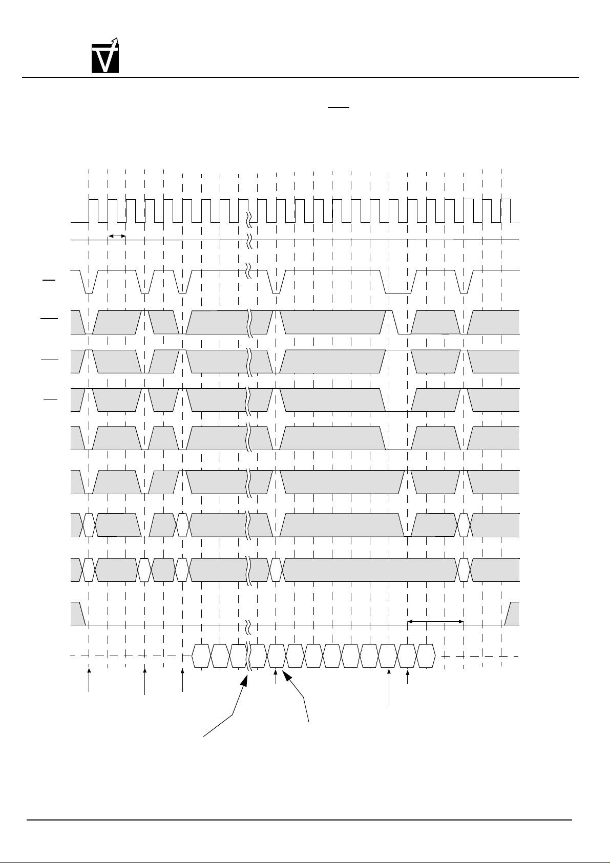
VG4616321B/VG4616322B
262,144x32x2-Bit
VIS
Figure 18.3. Full Page Read Cycle (Burst Length = Full Page, CAS Latency = 3)
Preliminary CMOS Synchronous Graphic RAM
T0 T1 T2 T3 T4 T5 T6 T7 T8 T9 T10 T11 T12 T13 T14 T15 T16 T17 T18 T19 T20 T21 T22
CLK
CKE
CS
RAS
CAS
WE
DSF
BS
High
t
CK3
A9
A0 ~ A8
DQM
DQ
RAx RBx
RAx
Hi-Z
Activate
Command
Bank A
CAx
Read
Command
Bank A
RBx
Ax
Ax+1
Activate
Command
Bank B
The burst counter wraps
from the highest order
page address back to zero
during this time interval
Ax+2
CBx
Ax-2
Ax-1
Read
Command
Bank B
Full Page burst operation does not terminate
when the burst length is satisfied; the burst
counter increments and continues bursting
beginning with the starting address.
Ax+1
Ax
Bx
Bx+1
Bx+2 Bx+3
Burst Stop
Command
Bx+4
Precharge
Command
Bank B
Bx+5
t
RP
RBy
RBy
Activate
Command
Bank B
Document:1G5-0145 Rev.1 Page 68
Page 69
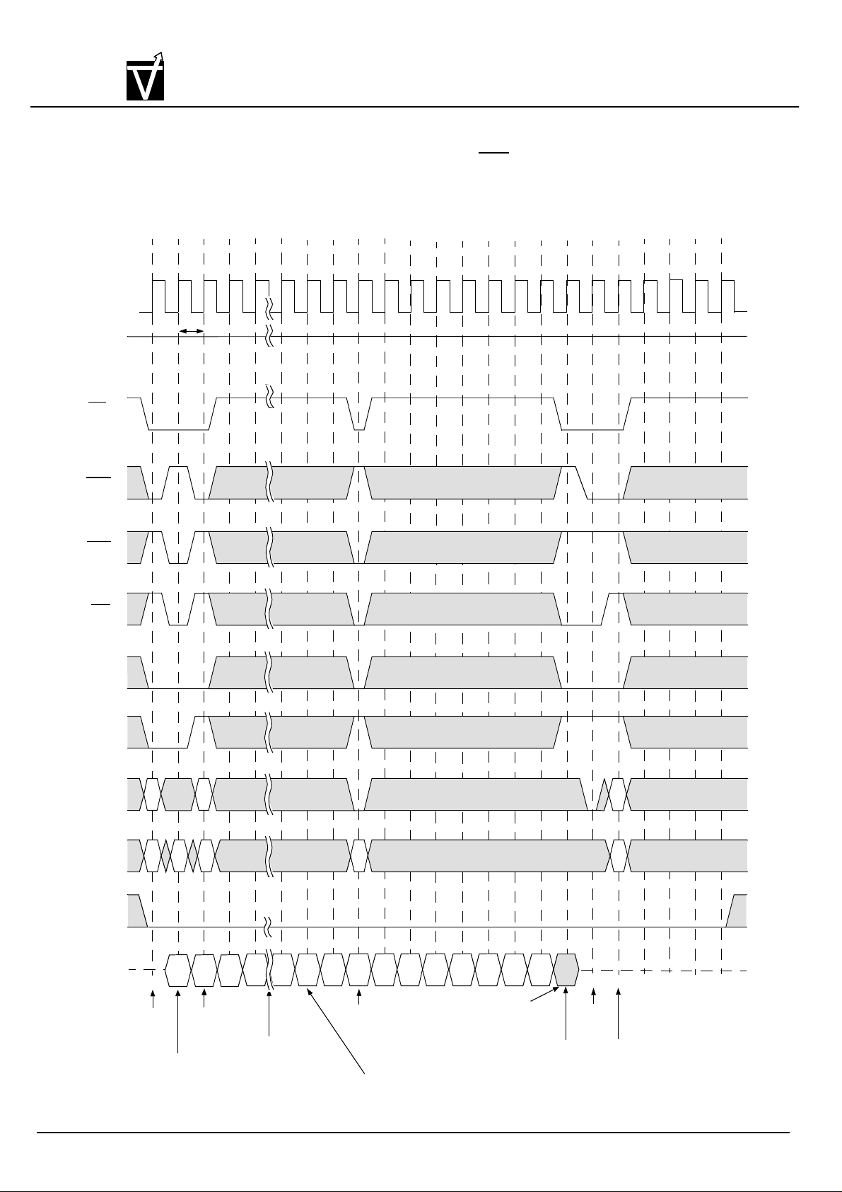
VG4616321B/VG4616322B
262,144x32x2-Bit
VIS
Figure 19.1 Full Page Write Cycle (Burst Length = Full Page, CAS Latency = 1)
CLK
CKE
CS
Preliminary CMOS Synchronous Graphic RAM
T0 T1 T2 T3 T4 T5 T6 T7 T8 T9 T10 T11 T12 T13 T14 T15 T16 T17 T18 T19 T20 T21 T22
t
CK1
High
RAS
CAS
WE
DSF
BS
A9
A0 ~ A8
RAx
RAx
CAx
RBx
RBx
CBx
RBy
RBy
DQM
Hi-Z
DQ
Activate
Command
Bank A
Command
Bank A
DAx
Write
DAx+1
DAx+2
Activate
Command
Bank B
The burst counter wraps
from the highest order
page address back to zero
during this time interval
DAx+3
DAx-1
DAx
DAx+1
Full Page burst operation does
not terminate when the burst
length is satisfied;the burst counter
increments and continues bursting
beginning with the starting address
DBx
Write
Command
Bank B
DBx+1 DBx+2
DBx+3
DBx+4
DBx+5 DBx+6
ignored
DBx+7
Data is
Burst Stop
Command
Precharge
Command
Bank B
Activate
Command
Bank B
Document:1G5-0145 Rev.1 Page 69
Page 70

VG4616321B/VG4616322B
262,144x32x2-Bit
VIS
Figure 19.2 Full Page Write Cycle (Burst Length = Full Page, CAS Latency = 2)
CLK
CKE
CS
Preliminary CMOS Synchronous Graphic RAM
T0 T1 T2 T3 T4 T5 T6 T7 T8 T9 T10 T11 T12 T13 T14 T15 T16 T17 T18 T19 T20 T21 T22
t
CK2
High
RAS
CAS
WE
DSF
BS
A9
A0 ~ A8
RAx
RAx
CAx
RBx
RBx
RBy
CBx RBy
DQM
DQ
Activate
Command
Bank A
DAx
Write
Command
Bank A
DAx+3
Activate
Command
Bank B
The burst counter wraps
from the highest order
page address back to zero
during this time interval
DAx-1
DAx
DAx+1 DBx
DBx+1
Write
Command
Bank B
Full Page burst operation does
not terminate when the burst
length is satisfied;the burst counter
increments and continues bursting
beginning with the starting address.
DBx+3 DBx+4 DBx+5
DBx+2
DBx+6
Data is ignored
Precharge
Command
Bank B
Burst Stop
Command
Activate
Command
Bank B
DAx+2
DAx+1
Document:1G5-0145 Rev.1 Page 70
Page 71

VG4616321B/VG4616322B
262,144x32x2-Bit
VIS
Figure19.3 Full Page Write Cycle (Burst Length = Full Page, CAS Latency = 3)
CLK
CKE
CS
Preliminary CMOS Synchronous Graphic RAM
T0 T1 T2 T3 T4 T5 T6 T7 T8 T9 T10 T11 T12 T13 T14 T15 T16 T17 T18 T19 T20 T21 T22
t
CK3
High
RAS
CAS
WE
DSF
BS
A9
A0 ~ A8
RAx
RAx RBx
CAx
RBx
CBx
RBy
RBy
DQM
Data is ignored
DQ
Hi-Z
Activate
Command
Bank A
Write
Command
Bank A
DAx+2
DAx+1DAx
DAx+3
Activate
Command
Bank B
The burst counter wraps
from the highest order
page addresss back to zero
during this time interval
DAx-1
DAx
DAx+1 DBx
DBx+1
DBx+2
DBx+3
Write
Command
Bank B
Full Page burst operation does
not terminate when the burst
length is satisfied;the burst counter
inrements and continues bursting
beginning with the starting address.
DBx+4
DBx+5
Precharge
Command
Bank B
Burst stop
Command
Activate
Command
Bank B
Document:1G5-0145 Rev.1 Page 71
Page 72
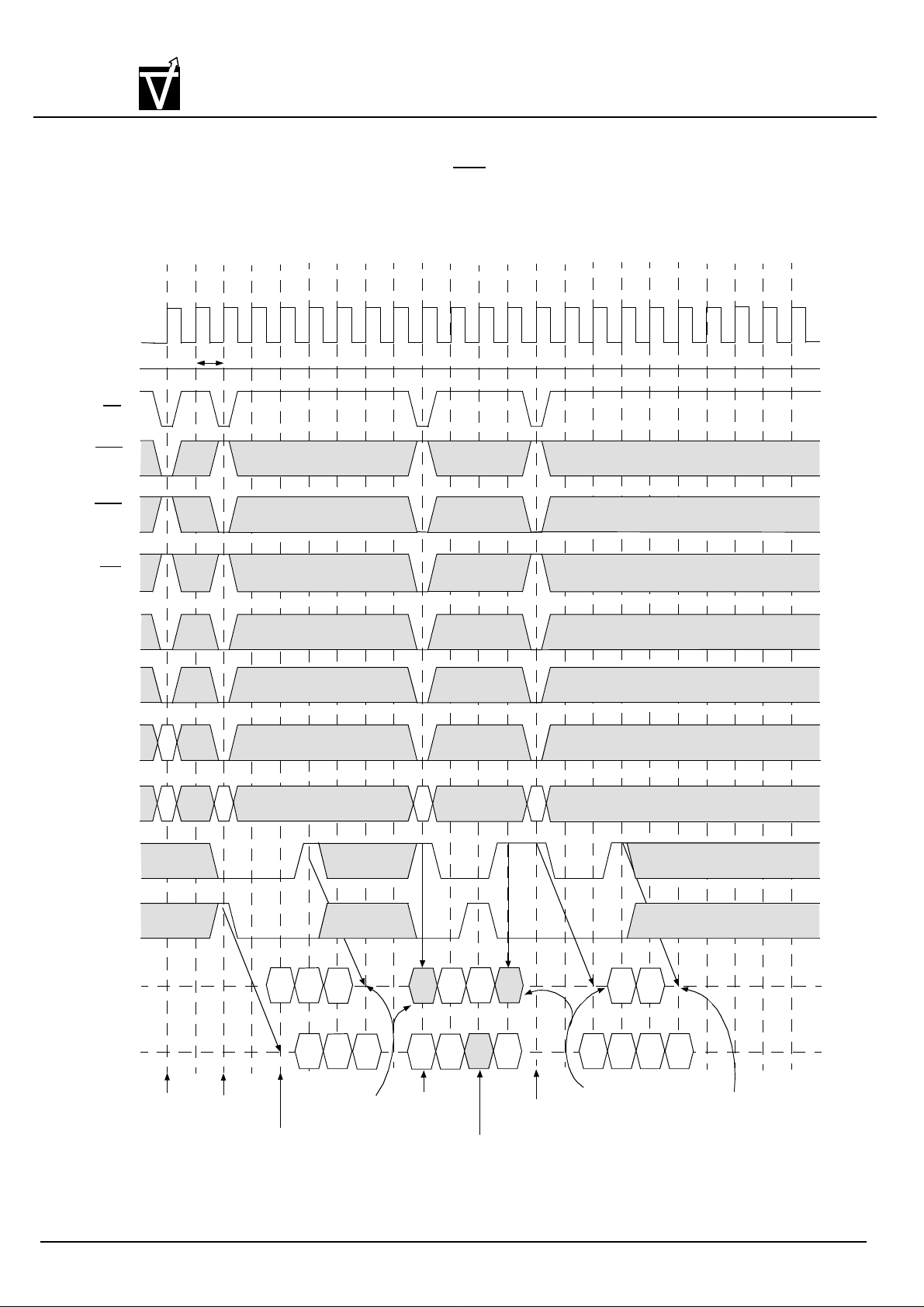
VG4616321B/VG4616322B
262,144x32x2-Bit
VIS
Figure 20. Byte Write Operation (Burst Length = 4, CAS Latency = 2)
Preliminary CMOS Synchronous Graphic RAM
T0 T1 T2 T3 T4 T5 T6 T7 T8 T9 T10 T11 T12 T13 T14 T15 T16 T17 T18 T19 T20 T21 T22
CLK
CKE
CS
RAS
CAS
WE
DSF
BS
A9
High
RAx
t
CK2
A0 ~ A8
RAx
CAx
CAy CAz
DQM0
DQM1~3
DQ0 - DQ7
DQ8 - DQ31
Hi-Z
Activate
Command
Bank A
Read
Command
Bank A
Ax0
Ax1
Upper 3 Bytes
are masked
Ax2
Ax2
Ax3 Az3
Lower Byte
is masked
DAy0 DAy1
Write
Command
Bank A
DAy2
DAy1
Upper 3 Bytes
are masked
DAy3
Command
Read
Bank A
Az1
Az0 Az1
Lower Byte
is masked
Az2
Az2
Lower Byte
is masked
Ax1
Document:1G5-0145 Rev.1 Page 72
Page 73
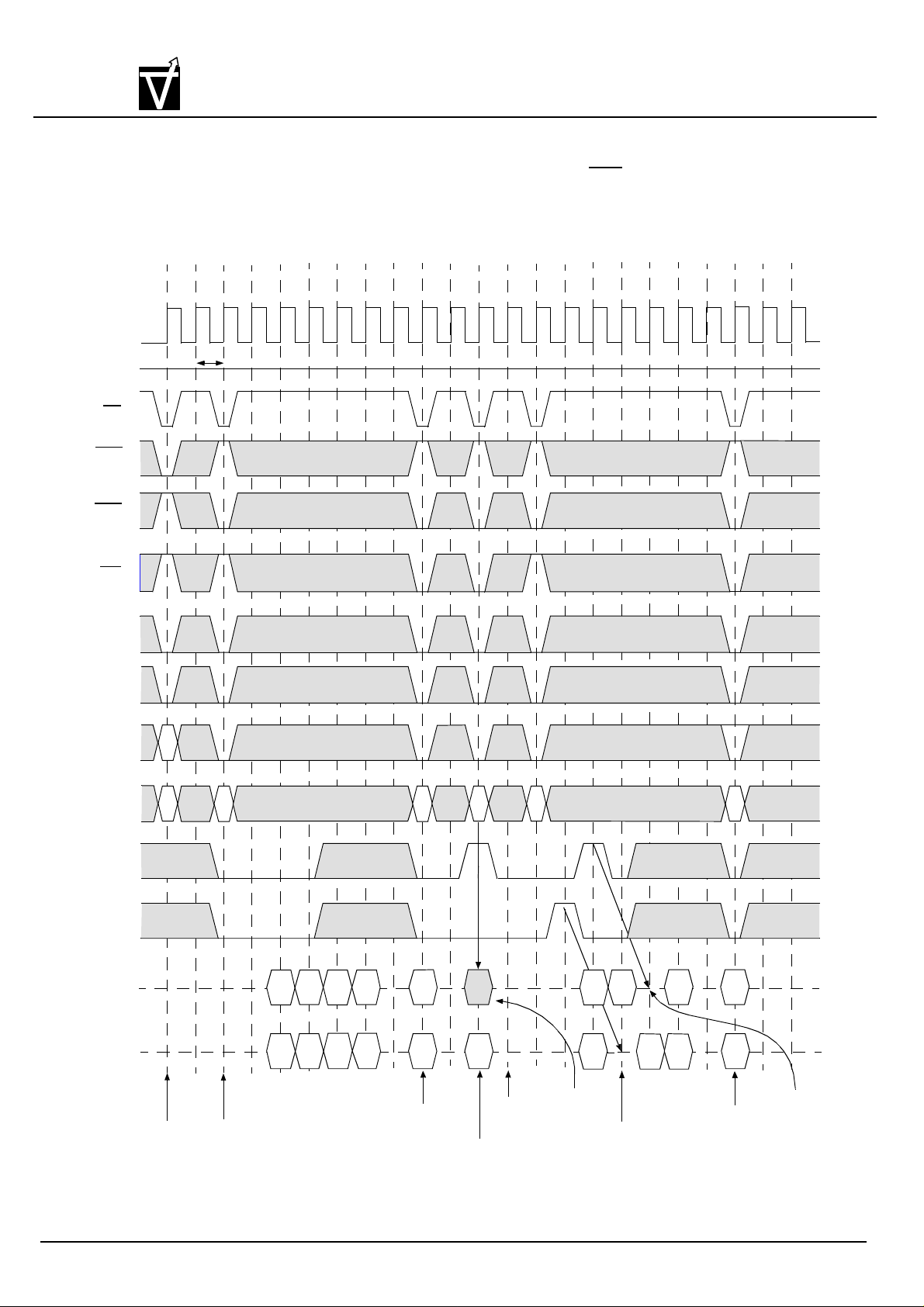
VG4616321B/VG4616322B
262,144x32x2-Bit
VIS
Figure 21. Burst Read and Single Write Operation (Burst Length = 4, CAS Latency = 2)
Preliminary CMOS Synchronous Graphic RAM
T0 T1 T2 T3 T4 T5 T6 T7 T8 T9 T10 T11 T12 T13 T14 T15 T16 T17 T18 T19 T20 T21 T22
CLK
CKE
CS
RAS
CAS
WE
DSF
BS
A9
High
RAx
t
CK2
A0 ~ A8
RAx
CAx
CAw CAy CAz
CAx
DQM0
DQM1~3
DQ0 - DQ7
DQ8 - DQ31
Hi-Z
Hi-Z
Activate
Command
Bank A
Read
Command
Bank A
Ax0
Ax1
Ax1 Ax2 Ax3 DQw0
Ax3
Ax2
DQw0
Single Write
Command
Bank A
Single Write
Command
Bank A
DQx0 Ay0
Read
Command
Bank A
Lower Byte
is masked
Ay1
Ay0
Upptr 3 Bytes
is masked
Ay3
Ay3Ay2Ax0
Az0
Az0
Single Write
Command
Bank A
Document:1G5-0145 Rev.1 Page 73
Lower Byte
is masked
Page 74
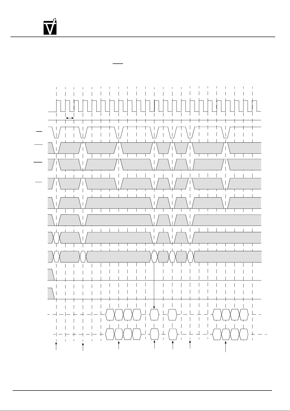
VG4616321B/VG4616322B
262,144x32x2-Bit
VIS
Figure 22. Full Page Burst Read and Single Write Operation
(Burst Length = Full Page, CAS Latency = 3)
Preliminary CMOS Synchronous Graphic RAM
T0 T1 T2 T3 T4 T5 T6 T7 T8 T9 T10 T11 T12 T13 T14 T15 T16 T17 T18 T19 T20 T21 T22
CLK
CKE
CS
RAS
CAS
WE
DSF
BS
A9
High
RAv
t
CK3
A0 ~ A8
RAv
CAv CAw
CAx
CAy
DQM0
DQM1~3
DQ0 - DQ7
DQ8 - DQ31
Activate
Command
Bank A
Read
Command
Bank A
Av0 Av1
Av0 Av1
Av2
Av2
Burst Stop
Command
Av3
Av3
DQw0
DQw0
Single Write
Command
Bank A
DQx0
DQx0 Av0
Single Write
Command
Bank A
Read
Command
Bank A
Av1
Av0
Av1
Burst Stop
Command
Av2
Av2
Av3
Av3
Document:1G5-0145 Rev.1 Page 74
Page 75
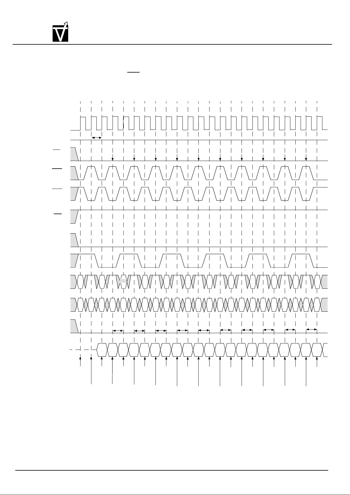
VIS
Figure 23. Random Row Read (lnterleaving Banks)
(Burst Length = 2, CAS Latency = 1)
CLK
CKE
CS
RAS
CAS
VG4616321B/VG4616322B
262,144x32x2-Bit
Preliminary CMOS Synchronous Graphic RAM
T0 T1 T2 T3 T4 T5 T6 T7 T8 T9 T10 T11 T12 T13 T14 T15 T16 T17 T18 T19 T20 T21 T22
t
CK1
High
Begin Auto
Precharge
Bank B
Begin Auto
Precharge
Bank A
Begin Auto
Precharge
Bank B
Begin Auto
Precharge
Bank A
Begin Auto
Precharge
Bank B
Begin Auto
Precharge
Bank A
Begin Auto
Precharge
Bank B
Begin Auto
Precharge
Bank A
Begin Auto
Precharge
Bank B
Begin Auto
Precharge
Bank A
WE
DSF
BS
A9
A0 ~ A8
DQM
DQ
RBu
RBu
Activate
Command
Bank B
Bank B
With Auto
Precharge
CBu RAu
Command
Read
RAu
Bu0
Activate
Bank A
CAu
t
RP
Activate
Command
Read
Bank A
With Auto
Precharge
RBv
RBv
Au0Bu1
Bank B
CBv
t
RP
Au1 Bv0
Activate
Command
Bank A
Read
Bank B
With Auto
Precharge
RAv
RAv
Bank A
With Auto
Precharge
CAv
Bv1
Read
RBw
RBw
t
RP
Av0
Activate
Command
Bank B
RAW
CBw
Av1
Command
Read
Bank B
With Auto
Precharge
CAw
RAw
t
RP
Bw0 Bx0
Bw1
Activate
Bank A
Read
Bank A
With Auto
Precharge
RBx RAx
RBx
t
RP
Aw0
Activate
Command
Bank B
Read
Bank B
With Auto
Precharge
CBx
t
RP
Aw1
Activate
Command
Bank A
RAx
CAx
t
RP
Bx1
Activate
Command
Bank B
Read
Bank A
With Auto
Precharge
RBy
CBy
RBy RAy
t
RP
Ax1
Ax0
Activate
Command
Bank A
Read
Bank B
With Auto
Precharge
RAy RBz RAz
RBz
By0
Bank A
With Auto
Precharge
CAy
By1
Command
Read
t
RP
Ay0
Activate
Bank B
CBz
t
RP
Ay1
Activate
Command
Bank A
Read
Bank B
With Auto
Precharge
RAz
Bz0
Document:1G5-0145 Rev.1 Page 75
Page 76
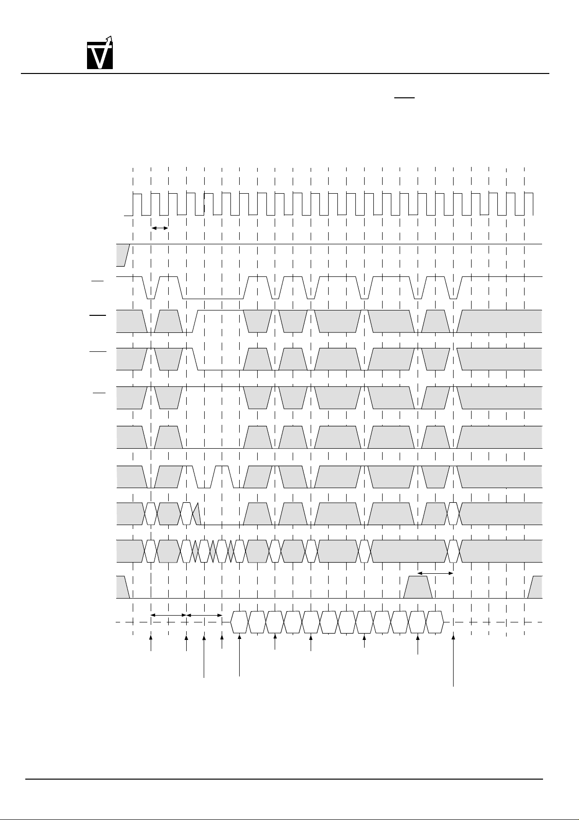
VIS
VG4616321B/VG4616322B
262,144x32x2-Bit
Preliminary CMOS Synchronous Graphic RAM
Figure 24. Full Page Random Column Read
(Burst Length = Full Page, CAS Latency = 2)
T0 T1 T2 T3 T4 T5 T6 T7 T8 T9 T10 T11 T12 T13 T14 T15 T16 T17 T18 T19 T20 T21 T22
CLK
t
CK2
CKE
CS
RAS
CAS
WE
DSF
BS
A9
A0 ~ A8
DQM
DQ
RAx
RAx
Activate
Command
Bank A
RBx
RBx
t
RRD
Activate
Command
Bank B
CAx
t
RCD
Read
Command
Bank B
Read
Command
Bank A
CBx
CAy CBy
Ay0
Bx0
Ax0 Bz1
Read
Command
Bank B
Read
Command
Bank A
Ay1
Read
Command
Bank A
CAz
By0
By1
CBz
Az0 Az1
Read
Command
Bank B
Az2
(Precharge Termination)
t
RP
Bz0
Precharge
Command Bank B
Bz2
RBw
RBw
Activate
Command
Bank B
Document:1G5-0145 Rev.1 Page 76
Page 77
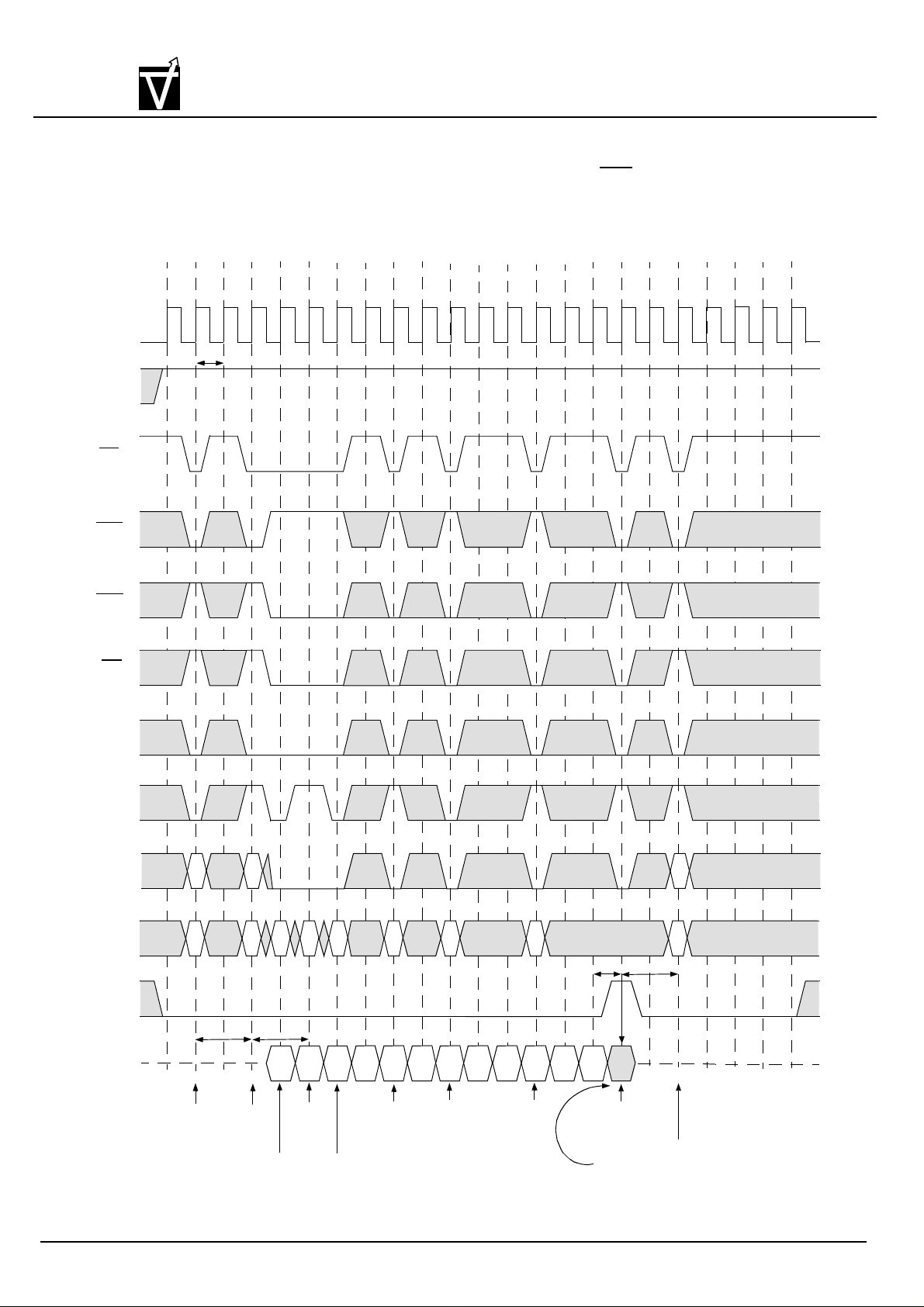
VG4616321B/VG4616322B
262,144x32x2-Bit
VIS
Figure 25. Full Page Random Column Write (Burst Length = Full Page, CAS Latency = 2)
CLK
CKE
CS
Preliminary CMOS Synchronous Graphic RAM
T0 T1 T2 T3 T4 T5 T6 T7 T8 T9 T10 T11 T12 T13 T14 T15 T16 T17 T18 T19 T20 T21 T22
t
CK2
RAS
CAS
WE
DSF
BS
A9
A0 ~ A8
RAx RBx
RAx
RBx CAx CBx
CAy CBy
RBw
CBz CAz
t
WR
RBw
t
RP
DQM
Activate
Command
Bank B
Command
t
RCD
DAx0
Write
Bank A
DBx0
Write
Command
Bank B
Command
DAy0
Write
Bank A
DAy1
Command
Bank B
DBy0 DBy1
Write
DAz0
Write
Command
Bank A
DAz1
DAz2
Write
Command
Bank B
DBz1
DBz0
(Precharge Termination)
DBz2
Precharge
Command Bank B
Write Data
is masked
Activate
Command
Bank B
DQ
Activate
Command
Bank A
t
RRD
Document:1G5-0145 Rev.1 Page 77
Page 78
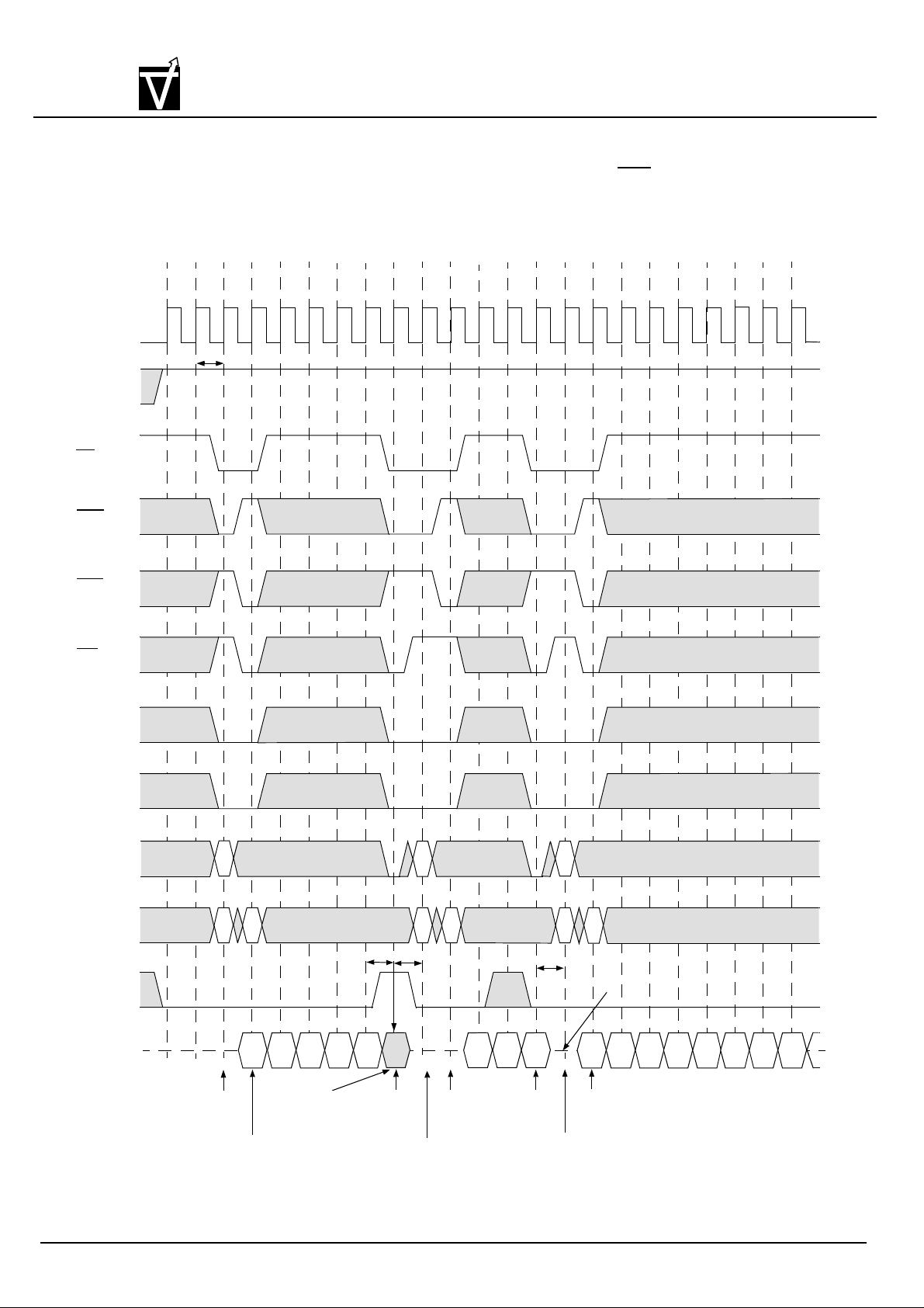
VG4616321B/VG4616322B
262,144x32x2-Bit
VIS
Figure 26.1. Precharge Termination of a Burst (Burst Length = Full Page, CAS Latency = 1)
Preliminary CMOS Synchronous Graphic RAM
T0 T1 T2 T3 T4 T5 T6 T7 T8 T9 T10 T11 T12 T13 T14 T15 T16 T17 T18 T19 T20 T21 T22
CLK
CKE
CS
RAS
CAS
WE
DSF
BS
t
CK1
A9
RAx
RAx
CAx
RAy
RAy
CAy
RAz
RAz
CAz
A0 ~ A8
tWR
t
DQM
DQ
Activate
Command
Bank A
Command
DAx0
Write
Bank A
DAx2DAx1
Precharge Termination
of a Write Burst.
Write data is masked.
DAx3
RP t
DAx4
Activate
Command
Bank A
Read
command
Bank A
Precharge
Command
Bank A
Ay0
Ay1
Precharge
Command
Bank A
Ay2
RP
Command
Activate
Command
Bank A
Precharge
Termination of
a Read Burst
DAz0
DAz1 DAz2
Write
Bank A
DAz3
DAz4
DAz5
DAz6
Document:1G5-0145 Rev.1 Page 78
DAz7
Page 79

VG4616321B/VG4616322B
262,144x32x2-Bit
VIS
Figure 26.2. Precharge Termination of a Burst
(Burst Length = 8 or Full Page, CAS Latency = 2)
Preliminary CMOS Synchronous Graphic RAM
T0 T1 T2 T3 T4 T5 T6 T7 T8 T9 T10 T11 T12 T13 T14 T15 T16 T17 T18 T19 T20 T21 T22
CLK
CKE
CS
RAS
CAS
WE
DSF
BS
High
t
CK2
A9
RAx
RAx
CAx
RAy
RAy
CAy
RAz
RAz
CAz
A0 ~ A8
tWR
t
RP
t
RP
t
RP
DQM
DQ
Activate
Command
Bank A
DAx0
Write
Command
Bank A
DAx1
DAx2
DAx3
Precharge
Command
Precharge Termination
of a Write Burst.
Write data is masked.
Bank A
Activate
Command
Bank A
Read
command
Bank A
Ay0
Precharge
Command
Bank A
Ay1
Ay2
Activate
Command
Bank A
Read
Command
Bank A
Precharge
Termination of
a Read Burst
DAz0
Precharge
Command
Bank A
DAz1
DAz2
Document:1G5-0145 Rev.1 Page 79
Page 80

VG4616321B/VG4616322B
262,144x32x2-Bit
VIS
Figure 26.3 Precharge Termination of a Burst
(Burst Length = 4, 8 or Full page, CAS Latency = 3)
Preliminary CMOS Synchronous Graphic RAM
T0 T1 T2 T3 T4 T5 T6 T7 T8 T9 T10 T11 T12 T13 T14 T15 T16 T17 T18 T19 T20 T21 T22
CLK
CKE
CS
RAS
CAS
WE
DSF
High
t
CK3
BS
A9
A0 ~ A8
RAx
RAx CAx
t
WR
RAy
RAy CAy
t
RP
RAz
RAz
t
RP
DQM
DQ
Activate
Command
Bank A
DAx0
Write
Command
Bank A
Write Data
is masked
DAx1
Precharge
Command
Bank A
Precharge Termination
of a Write Burst
Activate
Command
Bank A
Read
Command
Bank A
Ay0
Precharge
Command
Bank A
Ay1
Ay2
Activate
Command
Bank A
Precharge Termination
of a Write Burst
Document:1G5-0145 Rev.1 Page 80
Page 81
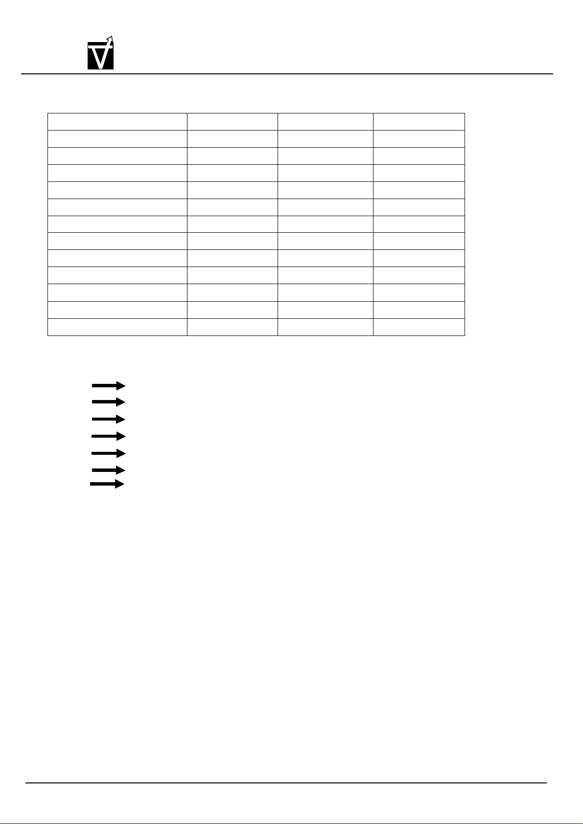
VG4616321B/VG4616322B
262,144x32x2-Bit
VIS
Ordering Information
VG4616321BQ-7 143MHz QFP Tray
VG4616321BQ-7R 143MHz QFP Tape & Reel
VG4616321BQ - 6 166MHz QFP Tray
VG4616321BQ - 6R 166MHz QFP Tape & Reel
VG4616321BQ - 5 200MHz QFP Tray
VG4616321BQ - 5R 200MHz QFP Tape & Reel
VG4616322BQ-7 143MHz QFP Tray
VG4616322BQ-7R 143MHz QFP Tape & Reel
VG4616322BQ-6 166MHz QFP Tray
VG4616322BQ-6R 166MHz QFP Tape & Reel
VG4616322BQ-5 200MHz QFP Tray
Preliminary CMOS Synchronous Graphic RAM
Part Number Frequency Package Packing Type
VG4616322BQ-5R 200MHz QFP Tape & Reel
VG4616321BQ - 7
• VG
• 46
•16321(2)
• B
• Q
• 7
• R
• VIS Memory Product
• Synchronous Graphic
• Sync, 2k self - ref. 512k x 32 SGRAM.16321 LVTTL, 16322 : SSTL-3
• Revision
• Package Type (Q : QFP)
• Speed (7 : 7ns, 6 : 6ns , 5 : 5ns)
• Packing Type (R : Tape & Reel, Blank : Tray)
Document:1G5-0145 Rev.1 Page 81
Page 82

VG4616321B/VG4616322B
DETAIL A
262,144x32x2-Bit
VIS
Outline Drawing Information
DIM
A
A1
A2
b
c
D
D1
E
E1
e
L1
θ
NOTE:
1. CONTROLLING DIMENSION : MILLIMETERS
2. DIMENSION D1 & E1 DO NOT INCLUDE MOLD PROTRUSION.
3. DIMENSION b DOES NOT INCLUDE DAMBAR PROTRUSION.
Preliminary CMOS Synchronous Graphic RAM
MILLIMETERS
MIN. NOM.
---
0.25
2.50
0.22
0.11
23.00
19.85
17.00
13.85
0.65 BASIC
0¢X ---
ALLOWABLE PROTRUSION IS 0.25mm PER SIDE.
DIMENSION D1 & E1 INCLUDE MOLD MISMATCH.
ALLOWABLE DAMBAR PROTRUSION SHALL NOT CAUSE THE
LEAD TO BE WIDER THAN THE MAXIMUM b DIMENSION BY
MORE THAN 0.08mm. DAMBAR CANNOT BE LOCATED ON THE
LOWER RADIUS OR THE FOOT.
---
---
2.70
---
0.15
23.20
20.00
17.20
14.00
0.880.73L
1.60 REF.
MAX. MIN.
3.40
2.90
0.38
0.23
23.40
20.15
17.40
14.15
7¢X 0¢X ---
D
INCHES
MAX.
NOM.
---
---
0.106
---
0.006
0.913
0.787
0.677
0.551
0.026 BASIC
0.063 REF.
0.134
0.114
0.015
0.009
0.921
0.793
0.685
0.557
0.0410.0350.0291.03
---
7¢X
---
---
0.010
0.098
0.009
0.004
0.906
0.781
0.669
0.545
80
81
100
1
SEATING PLANE
D1
51
50
A2
E
E1
A1
b L1
0.12mm
M
TYP.
c
A
L
θ
31
30
DETAIL A
e
0.08mm
e
Document:1G5-0145 Rev.1 Page 82
 Loading...