

Page 1

Preliminary VG37648041AT
VIS
CMOS Synchronous Dynamic RAM
Description
The 256Mb DDR SDRAM is a high-speed COMS, dynamic random-access memory containing
268,435,456 bits. It is internally configured as a quad-bank DRAM.
The 256Mb DDR SDRAM uses a double-data-rate architecture to achieve high-speed oper-
ation. The double data rate architecture is essentially a 2n prefetch architecture with an interface designed to transfer two data words per clock cycle at the I/O pins. A single read or write
access for the 256Mb DDR SDRAM effectively consists of a single 2n-bit wide, one clock cycle
data transfer at the internal DRAM core and two corresponding n-bit wide, one-half-clock-cycle
data transfers at the I/O pins.
A bidirectional data strobe (DQS) is transmitted externally, along with data, for use in data
capture at the receiver. DQS is an intermittent strobe transmitted by the DDR SDRAM during
READs and by the memory controller during WRITEs. DQS is edge-aligned with data for
READs and center-aligned with data for WRITEs.
The 256Mb DDR SDRAM operates from a differential clock (CLK and CLK#; the crossing of
CLK going HIGH and CLK# going LOW will be referred to as the postive edge of CLK). Commands (address and control signals) are registered at verey positive edge of CLK. Input data is
registered on both edges of DQS, and output data is referenced to both edges of DQS, as well
as to both edges of CLK.
Read and Write assesses to the DDR SDRAM are burst oriented; accesses start at a
selected location and continue for a programmed number of locations in a programmed
sequence. Accesses begin with the registration of an ACTIVE command, which is then followed
by a READ or WRITE command. The address bits registered coincident with the ACTIVE command are used to select the bank and row to be accessed (BA0,BA1 select the bank; A0-A12
select the row). The address bits registered coincident with sthe READ or WRITE command
are used to select the starting column location for the burst access.
The DDR SDRAM provides for programmable READ or WRITE burst lengths of 2,4 or 8
locations. An AUTO PRECHARGE function may be enabled to provide a selftimed row precharge that is initiated at the end of the burst access.
As with standard SDRAMs, the pipelined, multibank architecture of DDR SDRAMs allows
for concurrent operation, thereby providing high effective bandwidth by hiding row precharge
and activation time.
The 256Mb DDR SDRAM is designed to operate in either low-power memory systems. An
auto refresh mode is provided, along with a power-saving, power-down mode. All inputs are
compatible with the JEDEC Standard for SSTL_2. All outputs are SSTL_2, Class II compatible.
Initial devices will have a VDD supply of 3.3V (nominal). Eventually, all devices will migrate
to a VDD supply of 2.5V(nominal). During this initial period of product availability. this split will
be vendor and device specific.
This data sheet includes all features and functionality required for JEDEC DDR devices;
options not required but listed, are noted as such. Certain vendors may elect to offer a superset
of this specification by offering improved timing and/or including optional features. Users benefit
from knowing that any system design based on the required aspects of this specification are
supported by all DDR SDRAM vendors; conversely, users seeking to use any superset specifications bear the responsibility to verify support with individual vendors.
256M:x4, x8, x16
Document : 1G5-0157 Rev.1 Page 1
Page 2

±
±
Preliminary VG37648041AT
VIS
CMOS Synchronous Dynamic RAM
Note: The functionality described in, and the timing specifications included in this data
sheet are for the DLL Enabled mode of operation. This is the only normal operating
mode for these DDR devices.
Features
• Double-data-rate architecture: two data transfers per clock cycle
• Bidirectional, intermittent data strobe (DQS) is transmitted/received with data, to be used in
capturing data at the receiver
• DQS is edge-aligned with data for READs: center-aligned with data for WRITEs
• Differential clock inputs (CLK and CLK#)
• DLL aligns DQ and DQS transitions with CLK transitions
• Commands entered on each positive CLK edge; data referenced to both edges of DQS
• Four internal banks for concurrent operation
• Data mask (DM) for write data
• Burst lengths:2,4, or 8
• CAS Latency: 2 or 2.5
• AUTO PRECHARGE option for each burst access
• Auto Refresh and Self Refresh Modes
• 7.81us Auto Refresh Interval
• 2.5V (SSTL_2 compatible) I/O
256M:x4, x8, x16
• VDDQ=+2.5V 0.2V
• VDD=+3.3V 0.3V
Document : 1G5-0157 Rev.1 Page 2
Page 3
VIS
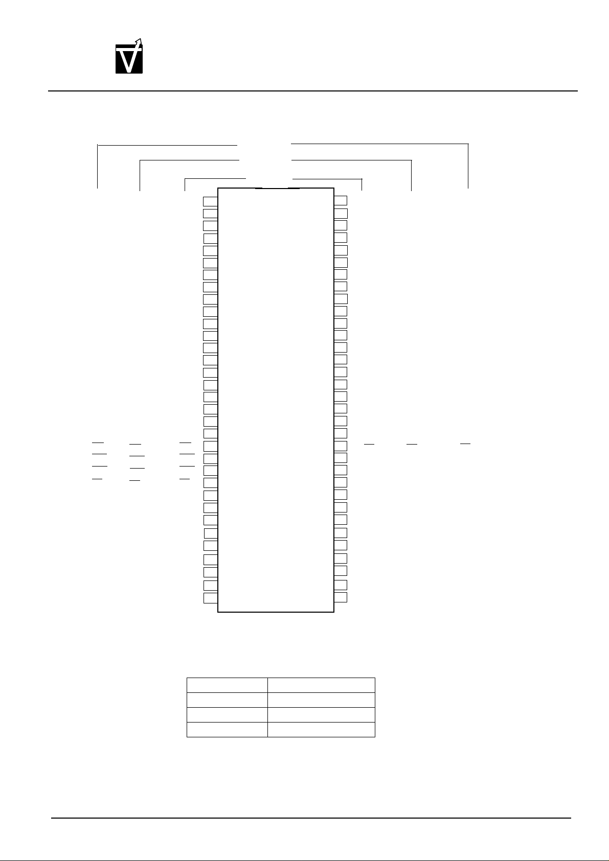
Pin Configuration
Preliminary VG37648041AT
256M:x4, x8, x16
CMOS Synchronous Dynamic RAM
256M DDR SDRAM (x4/x8/x16) Pin-out
64M X 4
32M X 8
16M X 16
V
DD
NC
V
DDQ
NC
DQ0
V
SSQ
NC
NC
V
DDQ
NC
DQ1
V
SSQ
NC
NC
V
DDQ
NC
NC
V
DD
NC
NC
WE
CAS
RAS
CS
NC
BA0
BA1
A10/AP
A
0
A
1
A
2
A
3
V
DD
V
DD
DQ0
V
DDQ
NC
DQ1
V
SSQ
NC
DQ2
V
DDQ
NC
DQ3
V
SSQ
NC
NC
V
DDQ
NC
NC
V
DD
NC
NC
WE
CAS
RAS
CS
NC
BA0
BA1
A10/AP
A
0
A
1
A
2
A
3
V
DD
V
DD
DQ0
V
DDQ
DQ1
DQ2
V
SSQ
DQ3
DQ4
V
DDQ
DQ5
DQ6
V
SSQ
DQ7
NC
V
DDQ
LDQS
NC
V
DD
NC
LDM
WE
CAS
RAS
CS
NC
BA0
BA1
A10/AP
A
0
A
1
A
2
A
3
V
DD
15
16
28
29
30
1
2
3
4
5
6
7
8
9
10
11
12
13
14
17
18
19
20
21
22
23
24
25
26
27
31
32
33
Top View
66 PIN TSOP(II)
(400 mil x 875 mil)
(0.65 mm PIN PITCH)
Bank Address:
BA0-BA1
Row Address:
A0-A12
Auto Precharge:
A10
66
65
64
63
62
61
60
59
58
57
56
55
54
53
52
51
50
49
48
47
46
45
44
43
42
41
40
39
38
36
35
34
V
SS
DQ15
V
SSQ
DQ14
DQ13
V
DDQ
DQ12
DQ11
V
SSQ
DQ10
DQ9
V
DDQ
DQ8
NC
V
SSQ
UDQS
NC
VREF
V
SS
UDM
CK
CK
CKE
NC
A
12
A
11
A
9
A
8
A
7
37
A
6
A
5
A
4
V
SS
V
SS
DQ7
V
SSQ
NC
DQ6
V
DDQ
NC
DQ5
V
SSQ
NC
DQ4
V
DDQ
NC
NC
V
SSQ
DQS
NC
VREF
V
SS
UD
CK
CK
CKE
NC
A
12
A
11
A
9
A
8
A
7
A
6
A
5
A
4
V
SS
V
SS
NC
V
SSQ
NC
DQ3
V
DDQ
NC
NC
V
SSQ
NC
DQ2
V
DDQ
NC
NC
V
SSQ
DQS
NC
VREF
V
SS
DM
CK
CK
CKE
NC
A
12
A
11
A
9
A
8
A
7
A
6
A
5
A
4
V
SS
Column Address Table
Organization Column Address
64Mx4 A0-A9,A11
32Mx8 A0-A9
16Mx16 A0-A8
Document : 1G5-0157 Rev.1 Page 3
Page 4
DQ3,DM
Preliminary VG37648041AT
VIS
CMOS Synchronous Dynamic RAM
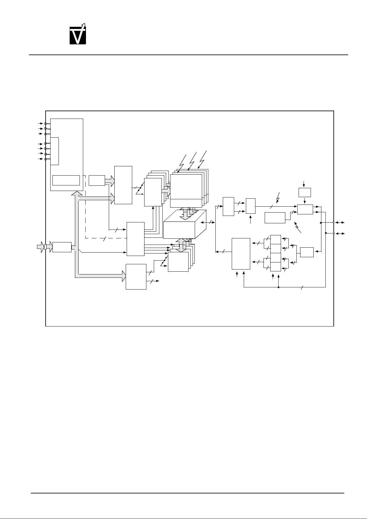
FUNCTIONAL BLOCK DIAGRAM- X4 CONFIGURATION
CKE
CLK#
CLK
COMMAND
DECODE
Generator
LOGIC
BANK1
BANK2
BANK3
CS#
WE#
CAS#
RAS#
256M:x4, x8, x16
A0-A12
BA0-BA1
MODE REGISTERS
ADDRESS
15
RESGISTER
REFRESH
13
COUNTER
13
13
11
ROW-
ADDRESS
MUX
2
2
CONTROL
LOGIC
13
BANK0
COLUMN
ADDRESS
COUNTER/
LATCH
BANK0
ROW-
ADDRESS
LATCH
&
DECODER
10
1
8192
SENSE AMPLIFIERS
SENSE AMPLIFIERS
I/O GATING
DM MASK LOGIC
COLUMN
DECODER
COL0
BANK0
BANK0
MEMORY
MEMORY
ARRAY
ARRAY
(8192x1024x8)
(8192x1024x8)
8192
(x8)
1024
DATA
8
READ
LATCH
4
WRITE
FIFO
&
DRIVERS
ctk
out
CLK
4
MUX
COL0
ctk
in
8
8
MASK
2
8
DATA
4
DQS
GENERATOR
INPUT
REGISTERS
1
1
4
4
COL0
CLK
DLL
DRVRS
1
DOS
1
1
1
RCVRS
4
4
4
1
DO0
DQS
Note 1: This Functional Block Diagram is intended to facilitate user understanding of the operation of the
device; it does not necessarily represent an actual circuit implementation.
Note 2: DM is a unidirectional signal (input only) but is internally loaded to match the load of the bidirectional
DQ and DQS signals.
Document : 1G5-0157 Rev.1 Page 4
Page 5
DQ7,DM
Preliminary VG37648041AT
VIS
CMOS Synchronous Dynamic RAM
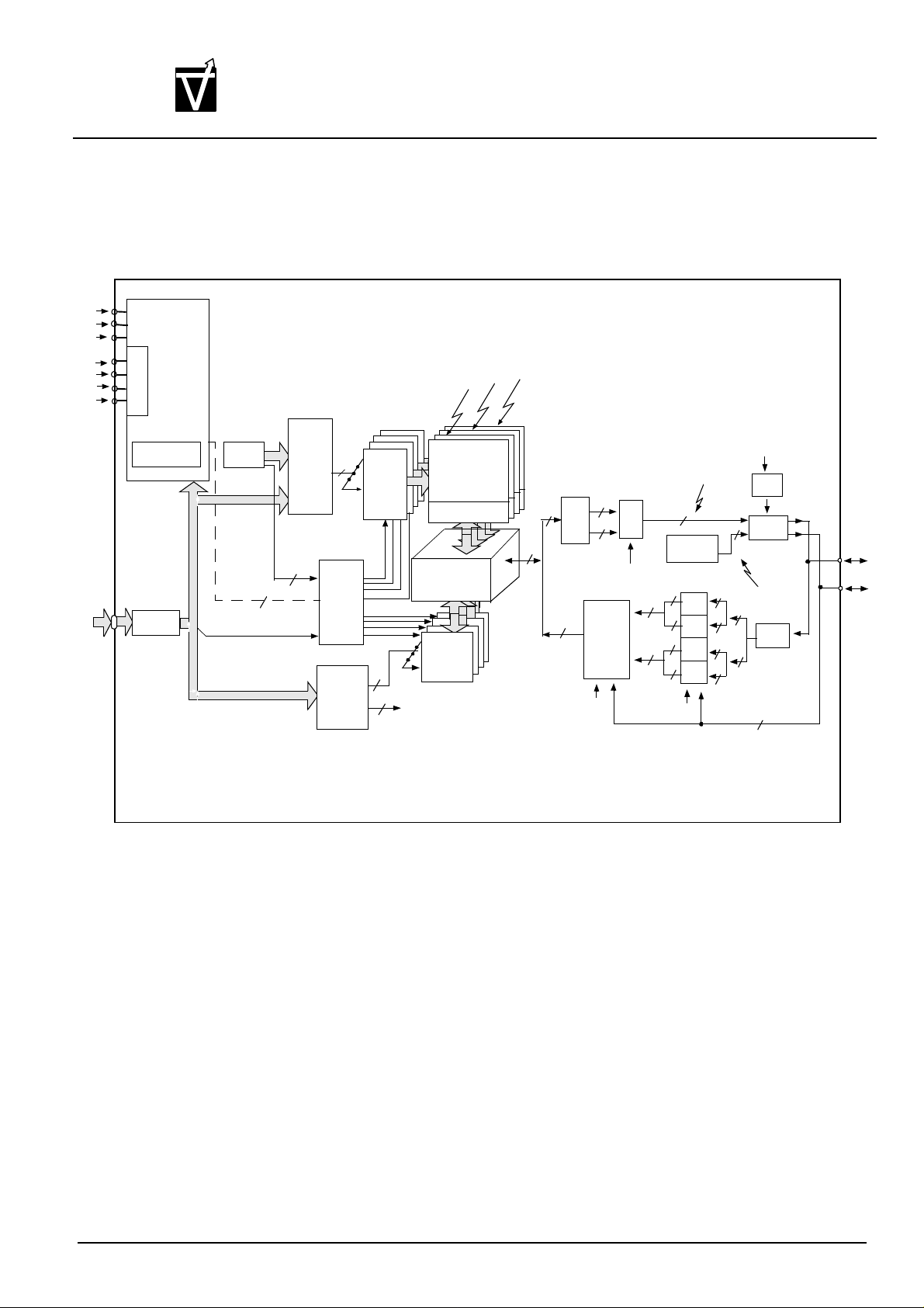
FUNCTIONAL BLOCK DIAGRAM- X8 CONFIGURATION
CKE
CLK#
CLK
COMMAND
DECODE
Generator
LOGIC
BANK1
BANK2
BANK3
CS#
WE#
CAS#
RAS#
256M:x4, x8, x16
A0-A12
BA0-BA1
MODE REGISTERS
ADDRESS
15
RESGISTER
REFRESH
13
COUNTER
13
13
10
ROW-
ADDRESS
MUX
2
2
CONTROL
LOGIC
13
COLUMN
ADDRESS
COUNTER/
LATCH
BANK0
ROW-
ADDRESS
LATCH
&
DECODER
9
1
8192
SENSE AMPLIFIERS
SENSE AMPLIFIERS
I/O GATING
DM MASK LOGIC BANK0
COLUMN
DECODER
COL0
BANK0
BANK0
MEMORY
MEMORY
ARRAY
ARRAY
(8192x512x16)
8192
512
(x16)
DATA
16
READ
LATCH
8
WRITE
FIFO
&
DRIVERS
ctk
out
CLK
8
MUX
COL0
ctk
in
16
16
MASK
2
16
DATA
4
DQS
GENERATOR
INPUT
REGISTERS
1
1
8
8
COL0
CLK
DLL
DRVRS
1
DQS
1
1
1
RCVRS
8
8
8
1
DO0
DQS
Note 1: This Functional Block Diagram is intended to facilitate user understanding of the operation of the
device; it does not necessarily represent an actual circuit implementation.
Note 2: DM is a unidirectional signal (input only)m but is internally loaded to match the load of the bidirec-
tional DQ and DQS signals.
Document : 1G5-0157 Rev.1 Page 5
Page 6
DQ15,LDM
Preliminary VG37648041AT
VIS
CMOS Synchronous Dynamic RAM
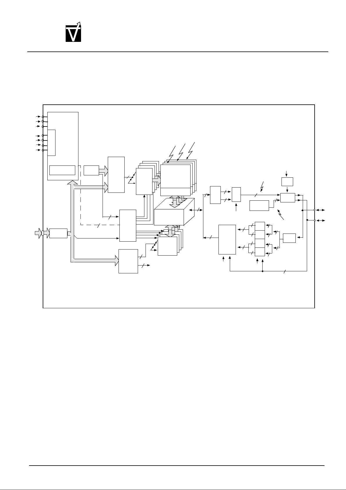
FUNCTIONAL BLOCK DIAGRAM- X16 CONFIGURATION
CKE
CLK#
CLK
COMMAND
DECODE
Generator
LOGIC
BANK1
BANK2
BANK3
CS#
WE#
CAS#
RAS#
256M:x4, x8, x16
A0-A12
BA0-BA1
MODE REGISTERS
ADDRESS
15
RESGISTER
REFRESH
13
COUNTER
13
13
9
ROW-
ADDRESS
MUX
2
2
CONTROL
LOGIC
13
COLUMN
ADDRESS
COUNTER/
LATCH
BANK0
ROW-
ADDRESS
LATCH
&
DECODER
8
1
8192
SENSE AMPLIFIERS
SENSE AMPLIFIERS
I/O GATING
DM MASK LOGIC BANK0
COLUMN
DECODER
COL0
BANK0
BANK0
MEMORY
MEMORY
ARRAY
ARRAY
(8192x256x32)
8192
256
(x32)
DATA
32
READ
LATCH
16
WRITE
FIFO
&
DRIVERS
ctk
out
CLK
16
MUX
COL0
ctk
in
32
32
MASK
2
32
DATA
16
DQS
GENERATOR
INPUT
REGISTERS
1
1
16
16
COL0
CLK
DLL
DRVRS
1
DQS
1
1
1
RCVRS
16
16
16
1
DO0 UDM
LDQS,
UDQS
Note 1: This Functional Block Diagram is intended to facilitate user understanding of the operation of the
device; it does not necessarily represent an actual circuit implementation.
Note 2: LDM and VDM are unidirectional signal (input only) but is internally loaded to match the load of the
bidirectional DQ and DQS signals.
Document : 1G5-0157 Rev.1 Page 6
Page 7
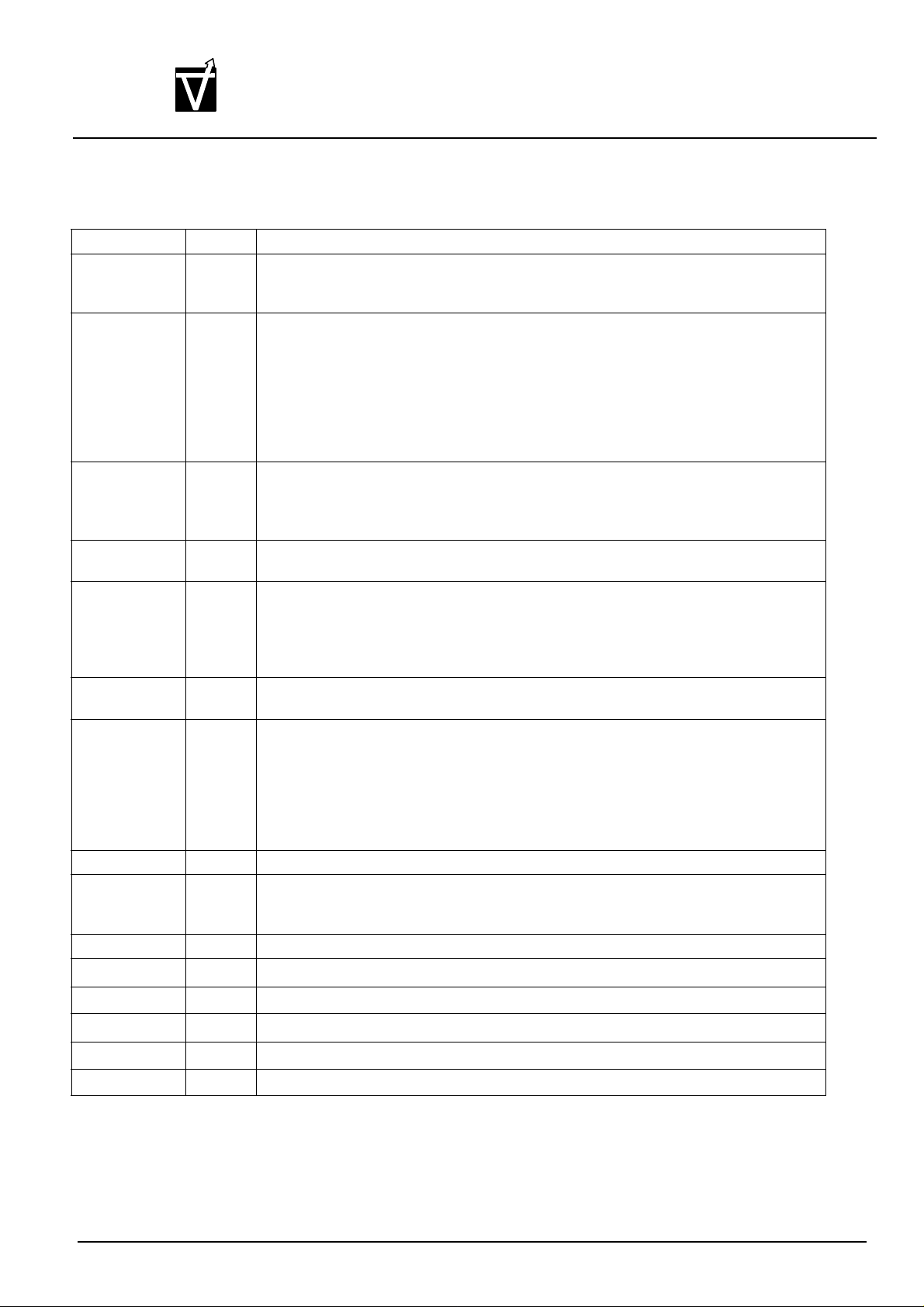
0.2V±0.3V
±
Preliminary VG37648041AT
VIS
256M:x4, x8, x16
CMOS Synchronous Dynamic RAM
PIN DESCRIPTIONS
Symbol Type Description
CLIK,CLK# Input Clock: CLK and CLK# are differential clock inputs. All address and control input signals
are sampled on the positive edge of CLK/negative edge of CLK#. Ouptut(read) data is
referenced to both edges of CLK. Internal clock signals are dervied from CLK/CLK#.
CKE Input Clock Enable: CKE HIGH activates, and CKE LOW deactivates internal clock signals,
and device input buffers and output drivers. Deactivating the clock provides PRECHARGE POWER-DOWN and SELF REFRESH operation (all banks idle), or ACTIVE
POWER-DOWN (row ACTIVE in any bank). CKE is synchronous for all functions
except for disabling outputs, which is achieved asynchronously. Input buffers, excluding
CLK, CLK# and CKE are disabled during power-down and self refresh modes, providing low standby power. CKE will recognize an LVCMOS LOW level prior to VREF being
stable on power-up.
CS# Input Chip Select: CS# enables (registered LOW) and disables (registered HIGH) the com-
mand decoder. All commands are masked when CS# is registered HIGH. CS# provides
for external bank selection on systems with multiple banks. CS# is considered part of
the command code.
RAS#,CAS#,
WE#
DM Input Input Data Mask: DM is an input mask signal for write data. Input data is masked when
BA0,BA1 Input Bank Address Inputs: BA0 and BA1 define to which bank an ACTIVE, READ, WRITE or
A0-A12 Input Address Inputs: Provide the row address for ACTIVE commands, and the column
DQ I/O Data Input/Output: Data bus
DQS I/O Data Strobe: Output with read data, input with write data. Edge-aligned with read data,
NC - No Connect: these pins should be left unconnected.
V
DDQ
V
SSQ
V
DD
V
SS
V
REF
Input Command Inputs: RAS#, CAS# and WE# (along with CS#) define the command being
entered.
DM is sampled HIGH along with that input data during a WRITE access. DM is sampled
on both edges of DQS. DM pins include dummy loading internally, to match the DQ and
DQS loading. For the x16, LDM corresponds to the data on DQ0-DQ7; UDM corresponds to the data on DQ8-DQ15.
PRECHARGE command is being applied.
address and AUTO PRECHARGE bit for READ/WRITE commands, to select one location out of the memory array in the respective bank. A10 is sampled during a PRECHARGE command to determine whether the PRECHARGE applies to one bank (A10
LOW) or all banks (A10 HIGH). If only one bank is to be precharged, the bank is
selected by BA0,BA1. The address inputs also provide the op-code durinbg a LOAD
MODE REGISTER command.
centered in write data. Used to capture write data. For the x16, LDQS corresponds to
the data on DQ0-DQ7; UDQS corresponds to the data on DQ8-DQ15.
Supply
Supply DQ Ground.
Supply
Supply Ground.
Input SSTL_2 reference voltage.
DQ Power Supply:+2.5V .
Power Supply: +3.3V .
Document : 1G5-0157 Rev.1 Page 7
Page 8

µ
µ
Preliminary VG37648041AT
VIS
CMOS Synchronous Dynamic RAM
Description
The 256Mb DDR SDRAM is a high-speed COMS, dynamic random-access memory containing
268,435,456 bits. The 256Mb DDR SDRAM is internally configured as a quad bank DRAM.
The 256Mb DDR SDRAM uses a double-data-rate architecture to achieve high-speed oper-
ation. The double data rate architecture is essentially a 2n prefetch architecture with an interface designed to transfer two data words per clock cycle at the I/O pins. A single read or write
access for the 256Mb DDR SDRAM effectively consists of a single 2n-bit wide, one clock cycle
data transfer at the internal DRAM core and two corresponding n-bit wide, one-half-clock-cycle
data transfers at the I/O pins.
Read and write accesses to the DDR SDRAM are burst oriented; accesses start at a
selected location and continue for a programmed number of locations in a programmed
sequence. Accesses begin with the registration of an ACTIVE command. which is then followed
by a READ or WRITE command. The address bits registered coincident with the ACTIVE command are used to select the bank and row to be accessed (BA0,BA1 select the bank; A0-A11
select the row). The address bits registered coincident with the READ or WRITE command are
used to select the starting column location for the burst access.
Prior to normal operation, the DDR SDRAM must be initialized. the following sections provide detailed information covering device initialization, register definition, command descriptions and device operation.
Initialization
256M:x4, x8, x16
DDR SDRAMs must be powered up and initialized in a predefined manner. Operational proce-
dures other than those specified may result in undefined operation. Power must first be applied to
VDD, then to V
to avoid device latch-up, which may cause permanent damage to the device. V
any time after V
are not recognized as valid until after V
LVCMOS LOW level after VDD is applied. Maintaining an LVCMOS LOW level on CKE during
power-up will put the DQ and DQS outputs in the High-Z stage, where they will remain until driven
in normal operation (by a read access). After all power supply and reference voltages are stable,
and the clock is stable, the DDR SDRAM requires a 200s delay prior to applying an executable
a command.
Once the 200s delay has been satisfied, a COMMAND INHIBIT or NOP comand should be
applied, and CKE should be brought HIGH. Following the NOP command, a PRECHARGE ALL
command should be applied. Next a LOAD MODE REGISTER command should be issued for the
Extended Mode Register to enable the DLL, then a LOAD MODE REGISTER comand should be
issued for the base mode Register, to reset the DLL, and to program the operating parameters.
200 clock cycles are required between the DLL reset and any read command. A PRECHARGE
ALL command should be applied, placing the device in the “all banks idle” stage.
, and finally to V
DDQ
, but is expected to be nominally coincident with VTT. Except for CKE, inputs
DDQ
(and to the system VTT). VTT must be applied after V
REF
can be applied
REF
is applied. CKE is an SSTL_2 input, but will detect an
REF
DDQ
Document : 1G5-0157 Rev.1 Page 8
Page 9

Preliminary VG37648041AT
VIS
CMOS Synchronous Dynamic RAM
Once in the idle state, two AUTO REFRESH cycles must be performed. Additionally, a LOAD
MODE REGISTER command for the base Mode Register, with the reset DLL bit deactivated (i.e.
to program operating parameters without resetting the DLL) must be performed. Following these
cycles, the DDR SDRAM is ready for normal operation.
Register Definition
Base Mode Register
The base mode register is used to define the specific mode of operation of the DDR SDRAM.
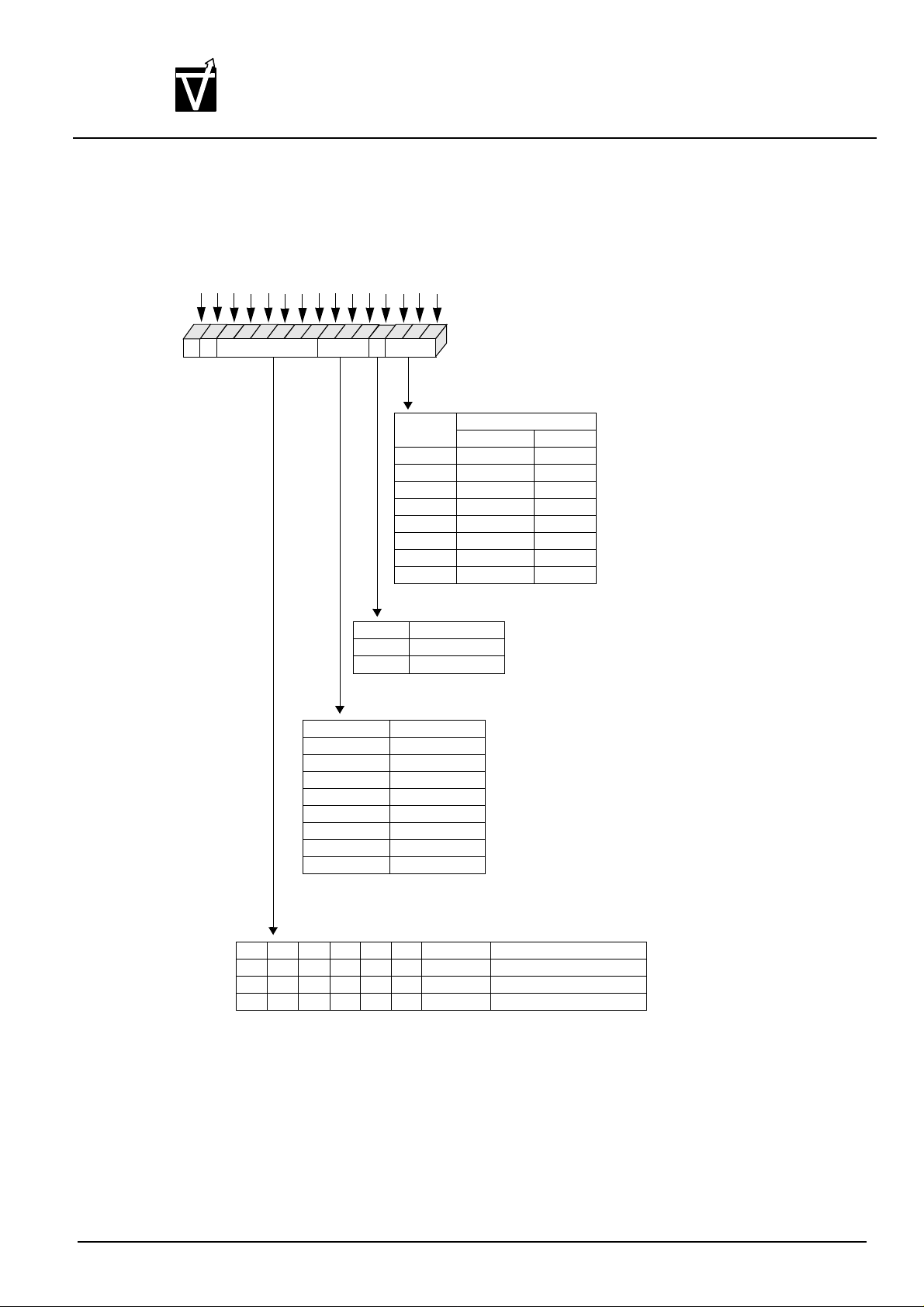
This definition includes the selection of a burst length, a burst type, a CAS latency, and an operating mode, as shown in Figure 1. The base mode register is programmed via the LOAD MODE
REGISTER command (with BA0=0 and BA1=0) and will retain the stored information unitil it is
programmed again or the device loses power.
Base mode register bits M0-M2 specify the burst length, M3 specifies the type of burst
(sequential or interleaved), M4-M6 specify the CAS latency, and M7-M11 specify the operating
mode.
The base mode register must be loaded when all banks are idle, and the controller must wait
the specified time before initiating the subsequent operation. Violating either of these requirements will result in unspecified operation.
256M:x4, x8, x16
Burst Length
Read and write accesses to the DDR SDRAM are burst oriented, with the burst length being
programmable, as shown in Figure 1. the burst length determines the maximum number of column locations that can be accessed for a given READ or WRITE command. Burst lengths of 2, 4,
or 8 locations are available for both the sequential and the interleaved burst types.
Reserved states should not be used, as unknown operation or incompatibility with future
versions may result.
When a READ or WRITE command is issued, a block of columns equal to the burst length is
effectively selected. All accesses for that burst take place within this block, meaning that the burst
will wrap within the block if a boundary is reached. The block is uniquely selected by A1-Ai when
the burst length is set to two, by A2-Ai when the burst length is set to four and by A3-Ai when the
burst length is set to eight (where Ai is the most significant column address bit for a given configuration). The remaining (least significant) address bit(s) is (are) used to select the starting location
within the block. The programmed burst length applies to both READ and WRITE bursts.
Document : 1G5-0157 Rev.1 Page 9
Page 10
VIS
Burst Type
Preliminary VG37648041AT
256M:x4, x8, x16
CMOS Synchronous Dynamic RAM
BA0
A12 A11 A10 A9 A8 A7 A6
BA0
14
12 11
13
0* 0*
* M13 and M14 (BA0 and BA1)
must be 0,0 to select the
base mode register (vs. the
extended mode register).
10
Operating Mode
A5
9 8 765
4 3 2 1
CAS Latency BT Burst Length
M6 M5 M4 CAS Latency
0 0 0 Reserved
0 0 1 Reserved
0 1 0 2
0 1 1 3(optional)
1 0 0 Reserved
1 0 1 1.5(optional)
1 1 0 2.5
1 1 1 Reserved
A3
A4
A2
M2 M1 M0
0 0 0 Reserved Reserved
0 0 1 2 2
0 1 0 4 4
0 1 1 8 8
1 0 0 Reserved Reserved
1 0 1 Reserved Reserved
1 1 0 Reserved Reserved
1 1 1 Reserved Reserved
M3 Burst Type
0 Sequential
1 Interleaved
A0
A1
0
Address Bus
Mode Register (Mx)
Burst Length
M3=0 M3=1
M12 M11 M10 M9 M8 M7 M6-10 Operating Mode
0 0 0 0 0 0 Valid Normal Operation
0 0 0 0 1 0 Valid Normal Operation/Reset DLL
- - - - - - - All other states reserved
Figure 1
BASE MODE REGISTER DEFINITION
Document : 1G5-0157 Rev.1 Page 10
Page 11
Preliminary VG37648041AT
VIS
CMOS Synchronous Dynamic RAM
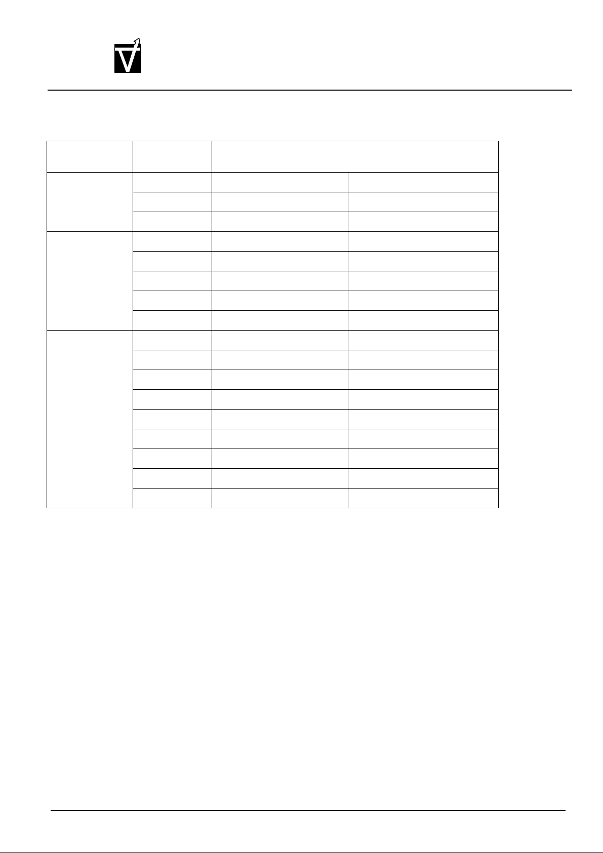
Table 1
BURST DEFINITION
Burst Length Starting Column
Address:
2
A1-A0
0 0 0-1-2-3 0-1-2-3
4
256M:x4, x8, x16
Order of Accesses Within a Burst
A0
0 0-1 0-1
1 1-0 1-0
0 1 1-2-3-0 1-0-3-2
1 0 2-3-0-1 2-3-0-1
1 1 3-0-1-2 3-2-1-0
A2 A1 A0
0 0 0 0-1-2-3-4-5-6-7 0-1-2-3-4-5-6-7
0 0 1 1-2-3-4-5-6-7-0 1-0-3-2-5-4-7-6
0 1 0 2-3-4-5-6-7-0-1 2-3-0-1-6-7-4-5
8
NOTE:
1. For a burst length of two, A1-Ai selects the two-data-element block; A0 selects the first access within the block.
2. For a burst length of four, A2-Ai selects the four-data-element block; A0-A1 selects the first access within the block.
3. For a burst length of eight, A3-Ai selects the eight-data-element block; A0-A2 selects the first access within the block.
4.Whenever a boundary of the block is reached within a given sequence above, the following access wraps within the
block.
0 1 1 3-4-5-6-7-0-1-2 3-2-1-0-7-6-5-4
1 0 0 4-5-6-7-0-1-2-3 4-5-6-7-0-1-2-3
1 0 1 5-6-7-0-1-2-3-4 5-4-7-6-1-0-3-2
1 1 0 6-7-0-1-2-3-4-5 6-7-4-5-2-3-0-1
1 1 1 7-0-1-2-3-4-5-6 7-6-5-4-3-2-1-0
Document : 1G5-0157 Rev.1 Page 11
Page 12
Preliminary VG37648041AT
VIS
256M:x4, x8, x16
CMOS Synchronous Dynamic RAM
Accesses within a given burst may be programmed to be either sequential or interleaved; this is referred
to as the burst type and is selected via bit M3.
The ordering of accesses within a burst is determined by the burst length, the burst type and the starting
column address, as shown in Table 1.
Read Latency
The READ latency is the delay, in clock cycles, between the registration of a READ command and the
availability of the first piece of output data. The latency can be set to 2 or 2.5 clocks (latencies of 1.5 or 3
are optional, and one or both of these optional latencies might be supported by some vendors).
If a READ command is registered at clock edge n, and the latency is m clocks, the data will be available
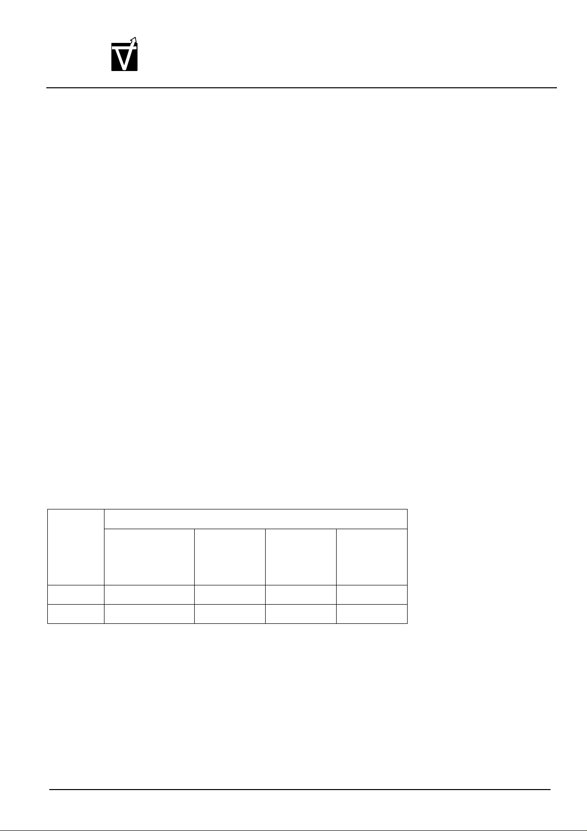
nominally coincident with clock edge n + m. Table 2 below indicated the operating frequencies at which
each CAS latency setting can be used.
Reserved stated should not be used as unknown operation, or incompatibility with future versions may
result.
Operating Mode
The normal operating mode is selected by setting M7-M12 to zero; to reset the DLL and select normal
operation , program M7, M9-M12 to 0 and M8 to 1. All other combinations of values for M7-M12 are
reserved for future use and/ or test modes.
Test Modes and reserved states should not be used because unknown operation or incompatibility with
future versions may result.
Table 2
CAS LATENCY
MAXIMUM OPERATING
CAS
LATENCY
SPEED
GRADE
-75 100 133 150 200
-8 100 125 143 166
=1.5
CAS
LATENCY
=2
CAS
LATENCY
=2.5
CAS
LATENCY
=3
* Values are nominal (i.e. may have been rounded off; exact tCK should be used)
Document : 1G5-0157 Rev.1 Page 12
Page 13
VIS
CLK#
CLK
Preliminary VG37648041AT
256M:x4, x8, x16
CMOS Synchronous Dynamic RAM
COMMAND
DQS
DQ
CLK#
CLK
COMMAND
READ NOP
CL=2
READ NOP
t
min
NOP
t
AC
max
AC
NOP
NOP
NOP
NOP
NOP
NOP
NOP
t
AC
CL=2.5
DQS
DQ
max
AC
DON’T CARE
UNDEFINED
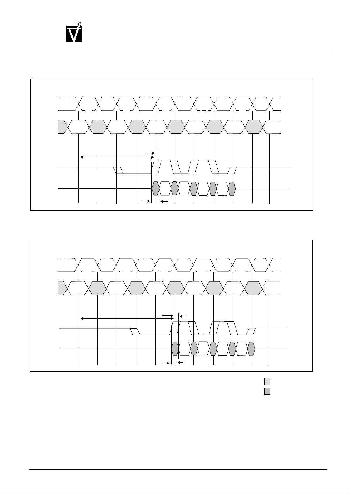
Burst Length=4 in the cases shown
Figure 2a
REQUIRED CAS LATENCIES
Document : 1G5-0157 Rev.1 Page 13
Page 14
VIS
CLK#
CLK
Preliminary VG37648041AT
256M:x4, x8, x16
CMOS Synchronous Dynamic RAM
COMMAND
DQS
DQ
CLK#
CLK
COMMAND
READ NOP
CL=1.5
READ NOP
t
min
NOP
t
AC
max
AC
NOP
NOP
NOP
NOP
NOP
NOP
NOP
CL=3
DQS
DQ
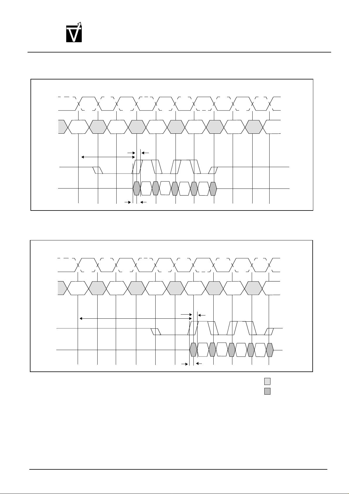
Burst Length=4 in the cases shown
t
AC
min
Figure 2b
OPTIONAL CAS LATENCIES
t
AC
max
DON’T CARE
UNDEFINED
Document : 1G5-0157 Rev.1 Page 14
Page 15
Preliminary VG37648041AT
VIS
256M:x4, x8, x16
CMOS Synchronous Dynamic RAM
EXTENDED MODE REGISTER
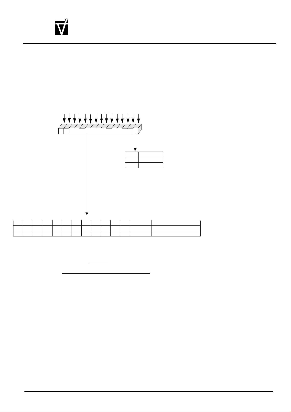
The Extended Mode Resister is used to enable or disable the DLL of the DDR SDRAM, as shown in Figure
3. The Extended Mode Register is programmed via the LOAD MODE REGISTER command (with BA0=1 and
BA1=0) and will retain the stored information until it is programmed again or the device loses power.
The Extended Mode Register must be loaded when all banks are idle, and the controller must wait the specified time before initiating the subsequent operation. Voolating either of these requirements will result in
unspecified operaiton.
BA0
BA1 A12
A11 A10A9A8
A6
A7
A4 A3
A5
A2 A1
A0
Address Bus
14
13 12 11 10
1*
0*
* E13 and E12 (BA0 and BA1)
must be 1,0 to select the
Extended Mode Register (vs. the
base Mode Register).
E12 E11 E10 E9 E8 E7 E6 E5 E4 E3 E2 E1 E0 Operating Mode
0 0 0 0 0 0 0 0 0 0 0 0 Valid Normal Operation
- - - - - - - - - - - - - All other stateds reserved
9
8 765
Operating Mode
4 321
0
Extended Mode Register (Ex)
DLL
E0 DLL
0 Enable
1 Disable
Figure 3
EXTENDED MODE REGISTER DEFINITION
Document : 1G5-0157 Rev.1 Page 15
Page 16
Preliminary VG37648041AT
VIS
256M:x4, x8, x16
CMOS Synchronous Dynamic RAM
COMMANDS
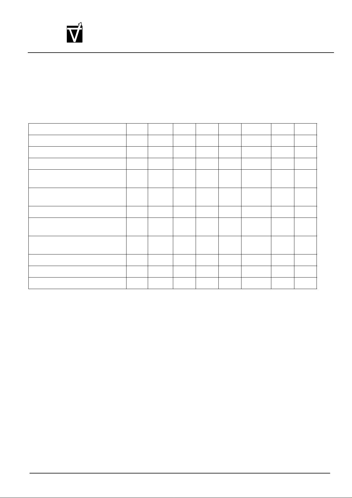
Truth Table 1 provides a quick reference of available commands. This is followed by a verbal description of
each command. Two additional Truth Tables appear following the Operation section; these tables provide current state/next state information.
TRUTH TABLE 1-Commands and DM Operation
(Notes:1)
Burst Length CS# RAS# CAS# WE# DM ADDR DQs NOTES
COMMAND INHIBIT (NOP) H X X X X X X
NO OPERATION (NOP) L H H H X X X
ACTIVE (Select bank and activate row) L L H H X Bank/Row X 3
READ (Select bank and column, and start
READ burst)
WRITE (Select bank and column, and
start WRITE burst)
BURST TERMINATE L H H L X X Active 9
PRECHARGE (Deactivate row in bank or
banks)
AUTO REFRESH or SELF REFRESH
(Enter self refresh mode)
LOAD MODE REGISTER L L L L X Op-Code X 2
Write Enable - - - - L - Active 8
Write Inhibit - - - - H - High-Z 8
NOTE: 1. CKE is HIGH for all commands shown except SELF REFRESH.
2. BA0-BA1 select either the Base or the Extended Mode Register (BA0=0, BA=1 selects Base
Mode Register; BA0=1, BA1=0 selects Extended Mode Register; other combinations of BA0-BA1
are reserved; A0-A12 provide the op-code to be written to the selected mode Register.
3. BA0-BA1 provide bank address and A0-A12 provide row address.
4. BA0-BA1 provide bank address; A0-Ai provide column address (where i=8 for x16, 9 for x8 and 11
for x4 except A10); A10 HIGH enables the auto precharge feature (nonpersistent), A10 LOW disables the auto precharge feature.
5. A10 LOW: BA0-BA1 determine which bank is precharged.
A10 HIGH: all banks are precharged and BA0-BA1 are “Don’t Care.”
6. This command is AUTO REFRESH if CKE is HIGH; SELF REFRESH if CKE is LOW.
7. Internal refresh counter controls row addressing; all inputs and I/Os are “Don’t Care” except for CKE.
8. Used to mask write data; provided conicident with the corresponding data.
9. Applies only to read bursts with autoprecharge disabled; this command is undefined (and should
not be used) for read bursts with autoprecharge enabled, and for write bursts
L H L H X Bank/col X 4
L H L L X Bank/Col Valid 4
L L H L X Code X 5
L L L H X X X 6,7
Document : 1G5-0157 Rev.1 Page 16
Page 17

Preliminary VG37648041AT
VIS
256M:x4, x8, x16
CMOS Synchronous Dynamic RAM
COMMAND INHIBIT
The COMMAND INHIBIT function prevents new commands from being executed by the DDR SDRAM.
The DDR SDRAM is effectively deselected. Operations already in progress are not affected.
NO OPERATION (NOP)
The NO OPERATION (NOP) command is used to perform a NOP to an DDR SDRAM which is selected
(CS# is LOW). This prevents unwanted commands from being registered during idle or wait states. Operations already in progress are not affected.
LOAD MODE REGISTER
The mode registers are loaded via inputs A0-A12 See mode register descriptions in the Register Defini-
tion section. The LOAD MODE REGISTER command can only be issued when all banks are idle, and a subsequent executable command cannot be issued until tMRD is met.
ACTIVE
The ACTIVE command is used to open (or activate) a row in particular bank for a subsequent access. The
value on the BA0, BA1 inputs selects the bank, and the address provided on inputs A0-A12 selects the row.
This row remains active (or open) for accesses until a PRECHARGE command is issued to that bank . A
PRECHARGE command must be issued befor opening a different row in the same bank.
READ
The READ command is used to initaiate a burst read access to an active row. The value on the BA0, BA1
inputs selects the bank, and the address provided on inputs A0-Ai(where i=8 for x 16, 9 for x8 or 11 for x 4,
except A10) selects the starting column location. The value on input A10 determines whether or not AUTO
PRECHARGE is used. If AUTO PRECHARGE is selected, the row being accessed will be precharged at the
end of the READ burst; if AUTO PRECHARGE is not selected, the row will remain open for subsequent
accesses.
WRITE
The WRITE command is used to initaiate a burst write access to an active row. The value on the BA0,
BA1 inputs selects the bank, and the address provided on inputs A0-Ai(where i=8 for x 16, 9 for 8 or 11 for x
4, except A10) selects the starting column location. The value on input A10 determines whether or not
AUTO PRECHARGE is used. If AUTO PRECHARGE is selected, the row being accessed will be precharged at the end of the WRITE burst; if AUTO PRECHARGE is not selected, the row will remain open for
subsequent accesses. Input data appearing on the DQs is written to the memory array subject to the DM
input logic level appearing coincident whith the data. If a given DM signal is registered LOW, the corresponding data will be written to memory; if the DM signal is registered HIGH, the corresponding data inputs
will be ignored, and a WRITE will not be executed to that byte/column location.
Document : 1G5-0157 Rev.1 Page 17
Page 18

µ
Preliminary VG37648041AT
VIS
256M:x4, x8, x16
CMOS Synchronous Dynamic RAM
PRECHARGE
The PRECHARGE command is used to deactivate the open row in a particular bank or the open row in all
banks. The bank(s) will be available for a subsequent row access a specified time (tRP) after the PRE-
CHARGE command is issued. Input A10 determines whether one or all banks are to be precharged, and in
the case where only one bank is to be precharged, inputs BA0, BA1 select the bank. Otherwise BA0, BA1
are treated as “Don’t Care.” Once a bank has been precharged, it is in the idle state and must be activated
prior to any READ or WRITE commands being issued to that bank.
AUTO PRECHARGE
AUTO PRECHARGE is a feature which performs the same individual-bank precharge function described
above, but without requiring an explicit command. This is accomplished by using A10 to enable AUTO PRECHARGE in conjunction with a specific READ or WRITE command. A precharge of the bank/row that is
addressed with the READ or WRITE command is automatically performed upon completion of the READ or
WRITE burst. AUTO PRECHARGE is nonpersistent in that it is either enabled or disabled for each individual
READ or WRITE command.
AUTO PRECHARGE ensures that the precharge is initiated at the earliest valid stage within a burst. The
user must not issue another command to the same bank until the precharge time (tRP) is completed. This is
determined as if an explicit PRECHARGE command was issued at the earliest possible time, as described
for each burst type in the Operation section of this data sheet.
BURST TERMINATE
The BURST TERMINATE command is used to truncate read bursts (with autoprecharge disabled). The
most recently registered READ command prior to the BURST TERMINATE command will be truncated, as
shown in the Operation section of this data sheet.
AUTO REFRESH
AUTO REFRESH is used during normal operation of the DDR SDRAM and is analagous to CAS#
BEFORE-RAS# (CBR) REFRESH in conventional DRAMs. This command is nonpersistent, so it must be
issued each time a refresh is required.
The addressing is generated by the internal refresh controller. This makes the address bits a “Don’t Care”
during an AUTO REFRESH command. The 256Mb DDR SDRAM requires AUTO REFRESH cycles at an
average interval of 7.81s(maximum).
Document : 1G5-0157 Rev.1 Page 18
Page 19

Preliminary VG37648041AT
VIS
256M:x4, x8, x16
CMOS Synchronous Dynamic RAM
SELF REFRESH
The SELF REFRESH command can be used to retain data in the DDR SDRAM, even if the rest of the
system is powered down. When in the self refresh mode,the DDr SDRAM retains data without external
clocking. The SELF REFRESH command is initiated like an AUTO REFRESH command except CKE is disabled (LOW). The DLL is automatically disabled upon entering SELF REFRESH, and is automatically
enabled upon exiting SELF REFRESH (200 clock cycles must then occur befor a READ command can be
issued). Input signals except CKE are “Don’t Care” during SELF REFRESH.
Once self refresh mode is engaged, the DDR SDRAM provides its own internal clocking, causing it to per-
form its own AUTO REFRESH cycles. The DDR SDRAM must remain in self refresh mode for a minimum
period equal to tRAS and may remain in self refresh mode for an indefinite period beyond that.
The procedure for exiting self refresh requires a sequence of commands. First, CLK must be stable prior
to CKE going back HIGH. Once CKE is HIGH, the DDR SDRAM must have NOP commands issued for
t
XSR because time is required for the completion of any internal refresh in progress. A simple algorithm for
meeting both refresh and DLL requirements is to apply NOPs for 200 clock cycles before applying any other
command.
OPERATIONS
BANK/ROW ACTIVATION
Before any READ or WRITE commands can be issued to a bank within the DDR SDRAM, a row in that
bank must be “opened.” This is accomplished via the ACTIVE command, which selects both the bank and
the row to be activated.
After opening a row (issuing an ACTIVE command). a READ or WRITE command may be issued to that
row, subject to the tRCD specification.
A subsequent ACTIVE command to a different row in the same bank can only be issued after the previous
active row has been “closed” (precharged). The minimum time interval between successive ACTIVE com-
mands to the same bank is defined by tRC.
A subsequent ACTIVE command to another bank can be issued while the first bank is being accessed,
which results in a reduction of total row-access overhead. The minimum time interval between successive
ACTIVE commands to different banks is defined by tRRD.
Document : 1G5-0157 Rev.1 Page 19
Page 20
VIS
Preliminary VG37648041AT
256M:x4, x8, x16
CMOS Synchronous Dynamic RAM
CLK#
CLK
CKE
HIGH
CS#
RAS#
CAS#
WE#
A0-A12
BA0,1
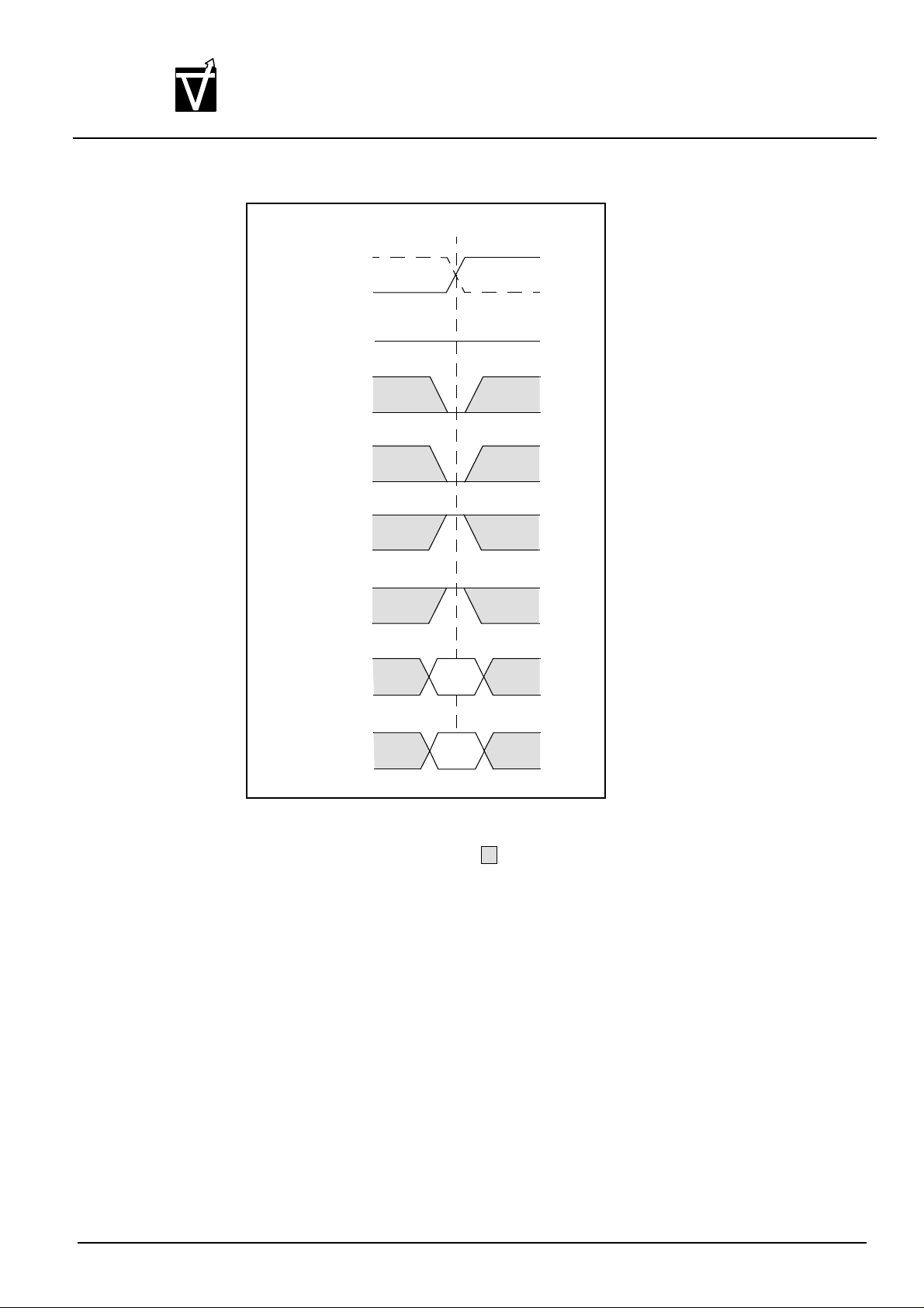
RA
BA
RA =Row Address
BA =Bank Address
=DON’T CARE
Figure 4
ACTIVATING A SPECIFIC ROW IN A SPECIFIC BANK
Document : 1G5-0157 Rev.1 Page 20
Page 21
VIS
CLK#
CLK
Preliminary VG37648041AT
256M:x4, x8, x16
CMOS Synchronous Dynamic RAM
COMMAND
A0-A12
BA0,BA1
ACT
Row
Bank x
NOP ACT
t
RRD
NOP
Row
Bank y
NOP
t
NOP
RCD
RD/
WR
Col
Bank y
DON’T CARE
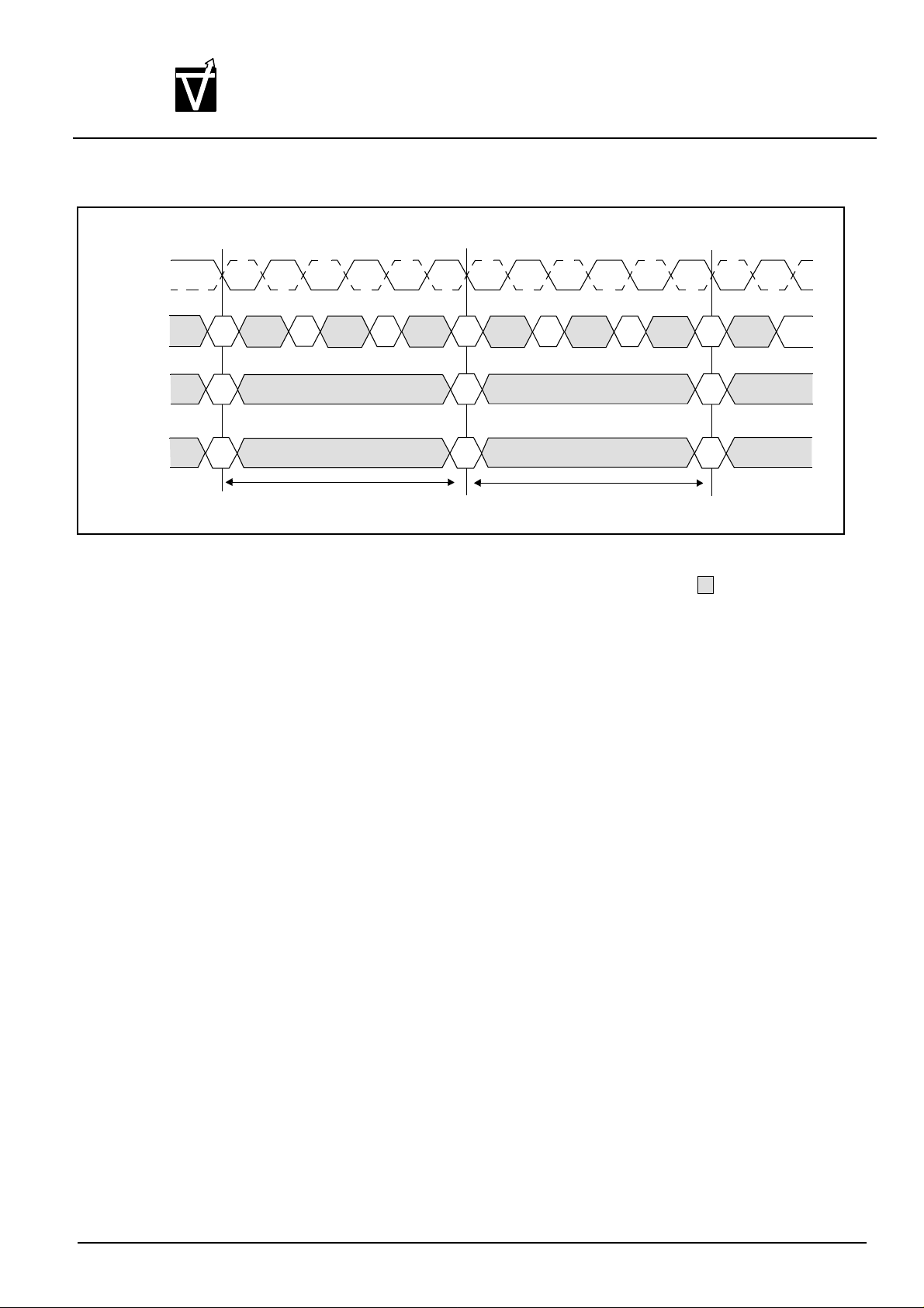
Figure 5
t
RCD
AND t
Definition
RRD
READs
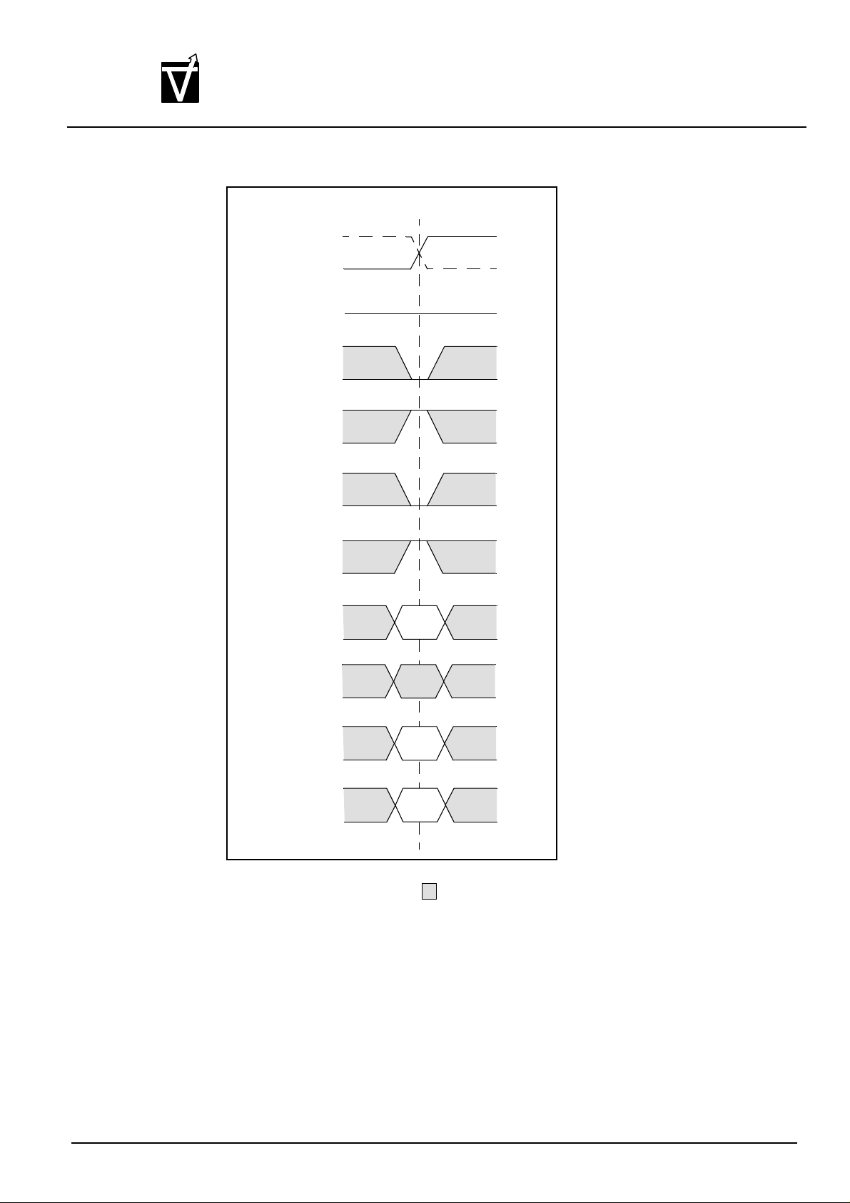
READ bursts are initiated with a READ command, as shown in Figure 6.
The starting column and bank addresses are provided with the READ command and AUTO PRECHARGE is
either enabled or disabled for that burst access. If AUTO PRECHARGE is enabled, the row being accessed is precharged at the completion of the burst. For the generic READ commands used in the following illustrations, AUTO
PRECHARGE is disabled.
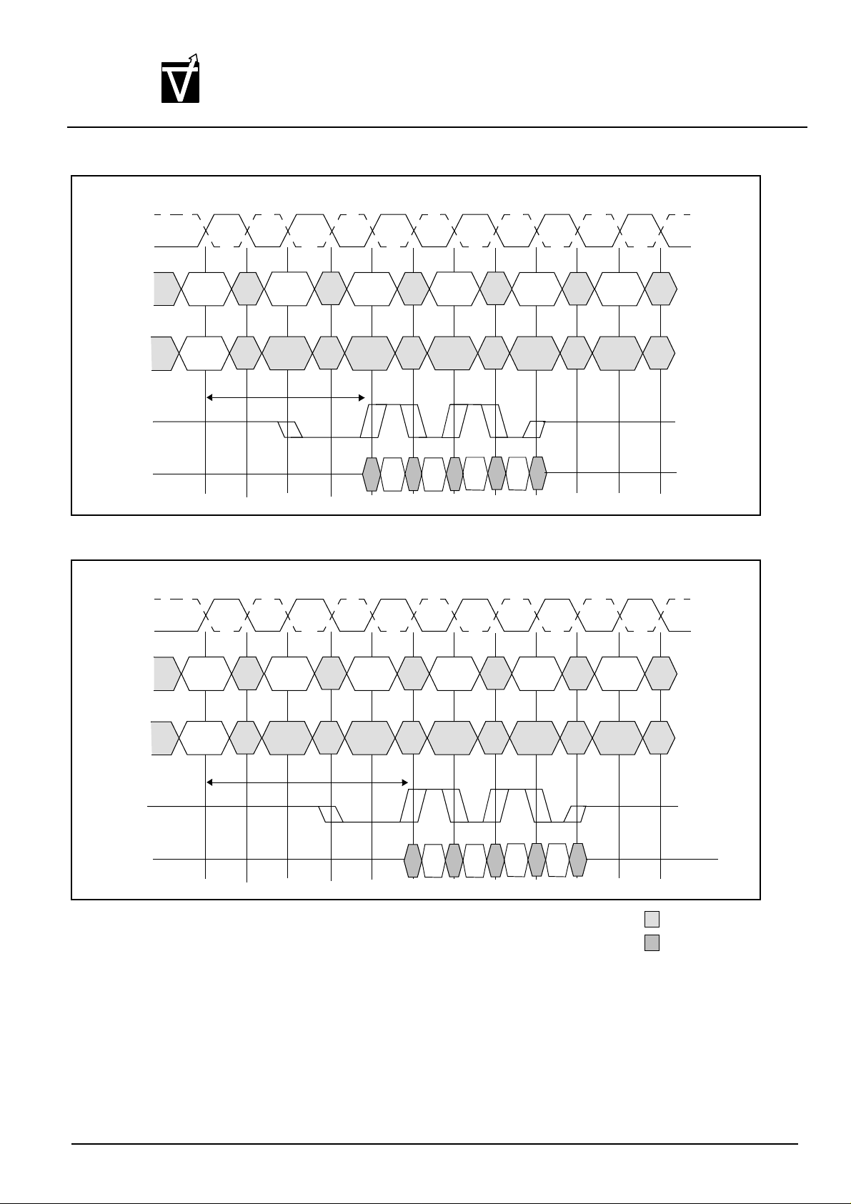
During READ bursts, the valid data-out element from the starting column address will be available following the
CAS latency after the READ command. Each subsequent data-out element will be valid nominally at the next positive or negative clock edge (i.e. at the next crossing of CLK and CLK#). Figure 7 shows general timing for each
posible CAS latency setting. DQS is driven by the DDR SDRAM along with output data. The initial LOW state on
DQS is known as the read preamble; the LOW state coincident with the last data-out element is known as the read
postamble.
Upon completion of a burst, assuming no other commands have been initiated, the DQs will go High-Z.
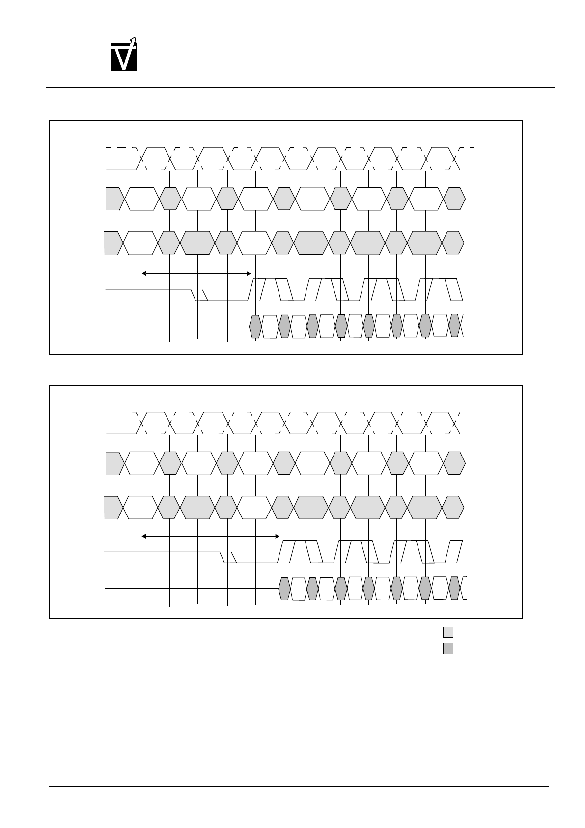
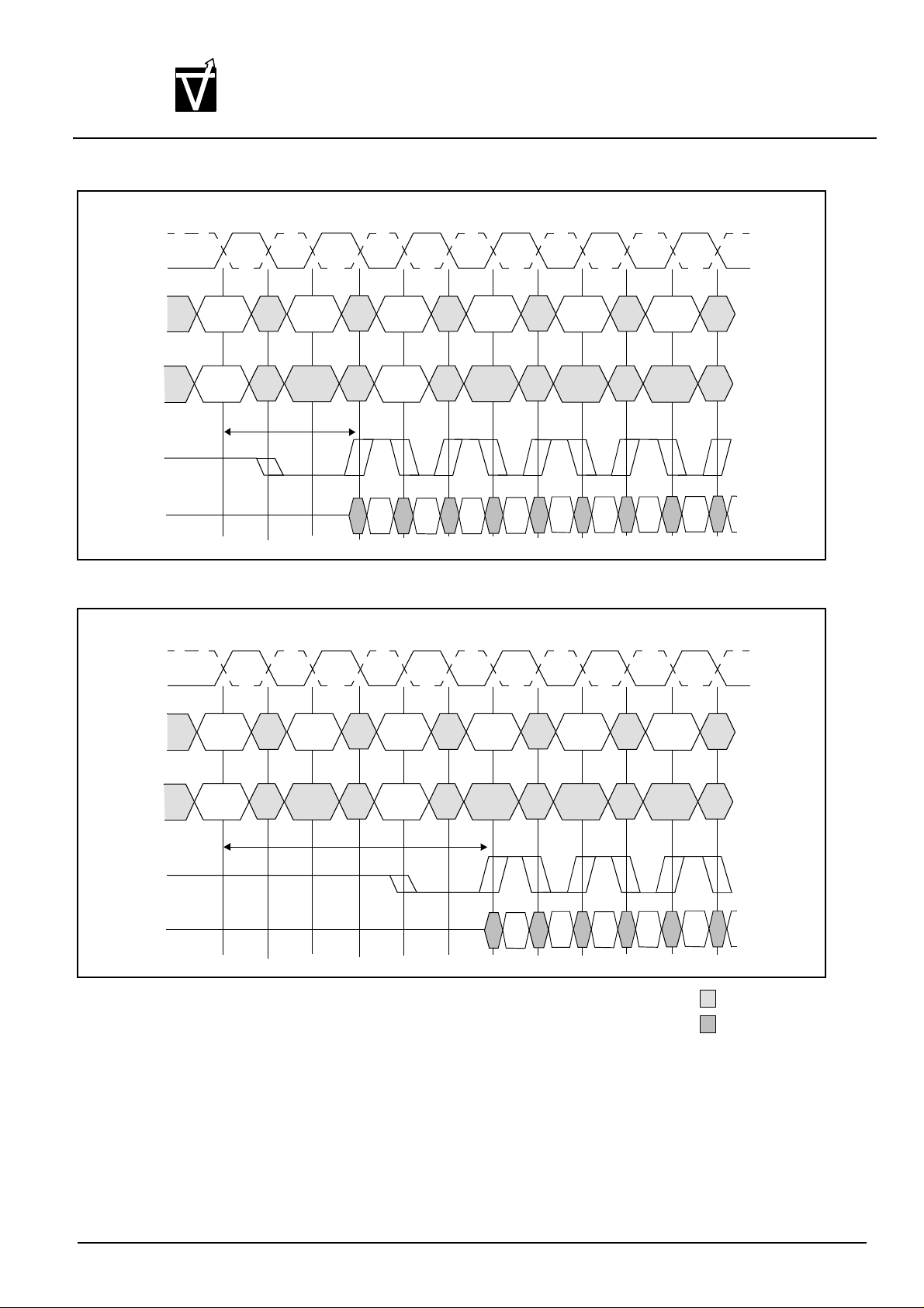
Data fom any READ burst may be concatenated with or truncated with data from a subsequent READ command. In either case, a continuous flow of data can be maintained. The first data element from the new burst follow either the last element of a completed burst or the last desired data element of a longer burst which is being
truncated. The new READ command should be issued x cycles after the first READ command, where x equals the
number of desired data element pairs (pairs are required by the 2n prefetch architecture). This is shown in Figure
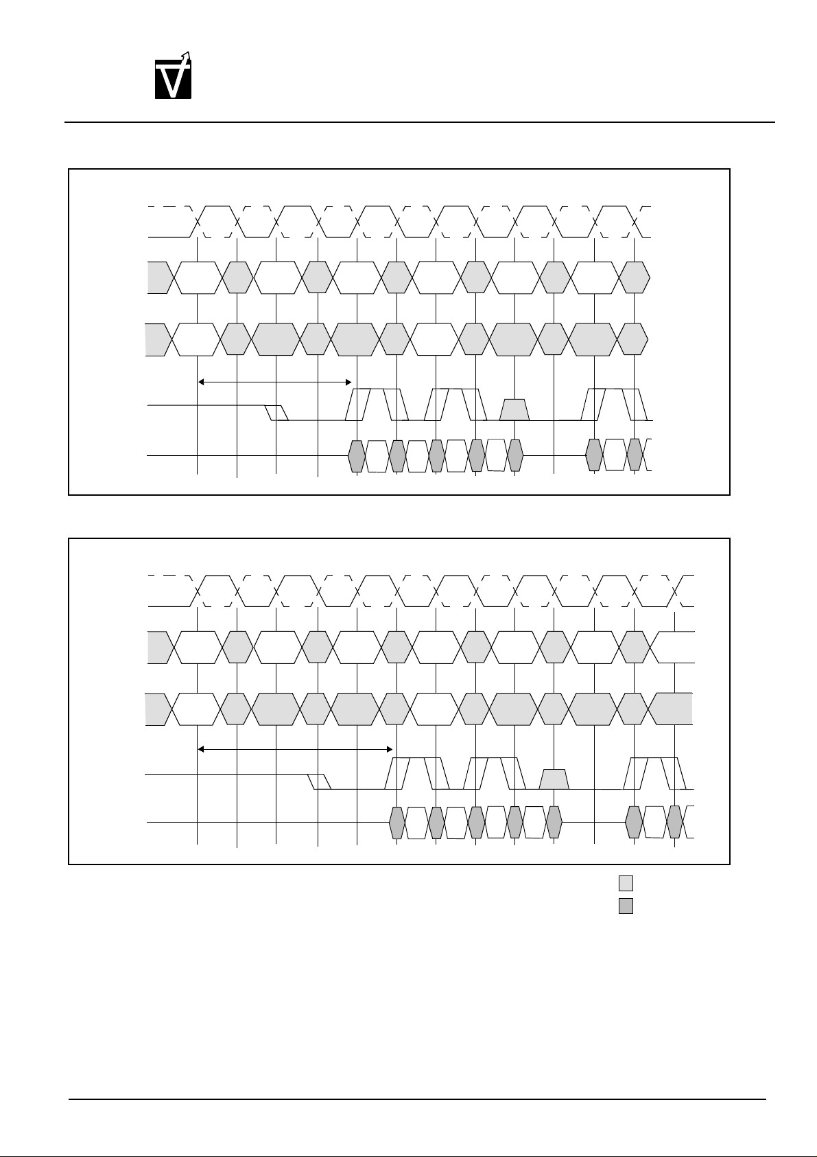
8. A READ command can be initiated on any clock cycle following a previous READ command. Non consecutive
READ data is shown for illustration in figure 9. Full-speed random read accesses within a page (or pages) can be
performed as shown in Figure 10.
NOP
Document : 1G5-0157 Rev.1 Page 21
Page 22
VIS
Preliminary VG37648041AT
256M:x4, x8, x16
CMOS Synchronous Dynamic RAM
CLK#
CLK
CKE
HIGH
CS#
RAS#
CAS#
WE#
x4:A0-A9
x8:A0-A8
x16:A0-A7
x4:A12
x8:A9,A12
x16:A8,A9,A12
A10
BA0,1
CA
EN AP
DIS AP
BA
=DON’T CARE
CA = Column Address
BA = Bank Address
EN AP = Enable Autoprecharge
DIS AP = Disable Autoprecharge
Figure 6
READ COMMAND
Document : 1G5-0157 Rev.1 Page 22
Page 23
VIS
CLK#
CLK
Preliminary VG37648041AT
256M:x4, x8, x16
CMOS Synchronous Dynamic RAM
COMMAND
ADDRESS
DQS
DQ
CLK#
CLK
COMMAND
READ
Bank a,
Col n
READ
CL=2
NOP
NOP
NOP
NOP
DO
n
NOP
NOP
NOP
NOP
NOP
NOP
ADDRESS
DQS
DQ
Bank a,
Col n
CL=2.5
DO
n
DO n=Data Out from column n
Burst Length=4
3 subsequent elements of Data Out appear in the programmed order following DO n
Figure 7a
READ BURST - REQUIRED CAS LATENCIES
DON’T CARE
UNDEFINED
Document : 1G5-0157 Rev.1 Page 23
Page 24
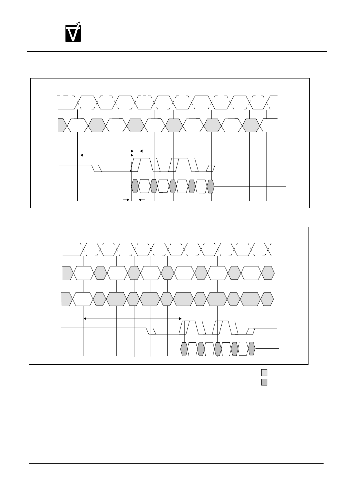
VIS
CLK#
CLK
Preliminary VG37648041AT
256M:x4, x8, x16
CMOS Synchronous Dynamic RAM
COMMAND
DQS
DQ
CLK#
CLK
COMMAND
READ NOP
CL=1.5
READ
NOP
t
min
NOP
t
AC
max
AC
NOP
NOP
NOP
NOP
NOP
NOP
NOP
ADDRESS
DQS
DQ
Bank a,
Col n
CL=3
n
DO
DO n=Data Out from column n
Burst Length=4
3 subsequent elements of Data Out appear in the programmed order following DO n
Figure 7b
READ BURST - OPTIONAL CAS LATENCIES
DON’T CARE
UNDEFINED
Document : 1G5-0157 Rev.1 Page 24
Page 25
VIS
CLK#
CLK
Preliminary VG37648041AT
256M:x4, x8, x16
CMOS Synchronous Dynamic RAM
COMMAND
ADDRESS
DQS
DQ
CLK#
CLK
COMMAND
READ
Bank,
Col n
READ
CL=2
NOP
NOP
READ
Bank,
Col b
READ
DO
n
NOP
NOP
NOP
NOP
DO
b
NOP
NOP
ADDRESS
DQS
DQ
Bank,
Col n
CL=2.5
Bank,
Col b
DO
n
DO
b
Do n(or b)= Data Out from column n (or column b)
Burst Length= 4 or 8 (if 4, the bursts are concatenated; if 8, the second burst interrupts the first)
3 subsequent elements of Data Out appear in the programmed order following DO n
3 (or 7) subsequent elements of Data Out appear in the programmed order following DO b
Figure 8a
CONSECUTIVE READ BURSTS - REQUIRED CAS LATENCIES
DON’T CARE
UNDEFINED
Document : 1G5-0157 Rev.1 Page 25
Page 26
VIS
CLK#
CLK
Preliminary VG37648041AT
256M:x4, x8, x16
CMOS Synchronous Dynamic RAM
COMMAND
ADDRESS
DQS
DQ
CLK#
CLK
COMMAND
READ
Bank,
Col n
READ
CL=1.5
NOP
NOP
DO
n
READ
Bank,
Col b
READ
NOP
NOP
NOP
NOP
b
NOP
DO
NOP
ADDRESS
DQS
DQ
Bank,
Col n
CL=3
Bank,
Col b
DO
n
Do n(or b)= Data Out from column n (or column b)
Burst Length= 4 or 8 (if 4, the bursts are concatenated; if 8, the second burst interrupts the first)
3 subsequent elements of Data Out appear in the programmed order following DO n
3 (or 7) subsequent elements of Data Out appear in the programmed order following DO b
Figure 8b
CONSECUTIVE READ BURSTS - OPTIONAL CAS LATENCIES
DO
b
DON’T CARE
UNDEFINED
Document : 1G5-0157 Rev.1 Page 26
Page 27
VIS
CLK#
CLK
Preliminary VG37648041AT
256M:x4, x8, x16
CMOS Synchronous Dynamic RAM
COMMAND
ADDRESS
DQS
DQ
CLK#
CLK
COMMAND
READ
Bank,
Col n
READ
CL=2
NOP
NOP
NOP
NOP
DO
n
READ
Bank,
Col b
READ
NOP
NOP
NOP
NOP
DO
b
NOP
ADDRESS
DQS
DQ
Bank,
Col n
CL=2.5
DO
n
Bank,
Col b
DO
b
DON’T CARE
UNDEFINED
DO n(or b)=Data Out from column n (or column b)
Burst Length=4
3 Subsequent elements of Data Out appear in the programmed order following DO n(and following DO b)
Figure 9a
NON-CONSECUTIVE READ BURSTS-REQUIRED CAS LATENCIES
Document : 1G5-0157 Rev.1 Page 27
Page 28
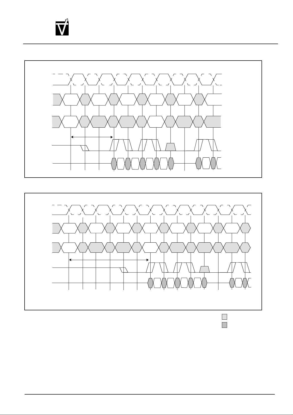
VIS
CLK#
CLK
Preliminary VG37648041AT
256M:x4, x8, x16
CMOS Synchronous Dynamic RAM
COMMAND
ADDRESS
DQS
DQ
CLK#
CLK
COMMAND
READ
Bank,
Col n
READ
CL=1.5
NOP
NOP
DO
n
NOP
NOP
DO
b
NOP
NOP
NOP
READ
Bank,
Col b
READ
NOP
NOP
ADDRESS
DQS
DQ
Bank,
Col n
CL=3
Bank,
Col b
n
DO
DO
b
DON’T CARE
UNDEFINED
DO n(or b)=Data Out from column n (or column b)
Burst Length=4
3 Subsequent elements of Data Out appear in the programmed order following DO n(and following DO b)
Figure 9b
NON-CONSECUTIVE READ BURSTS-OPTIONAL CAS LATENCIES
Document : 1G5-0157 Rev.1 Page 28
Page 29
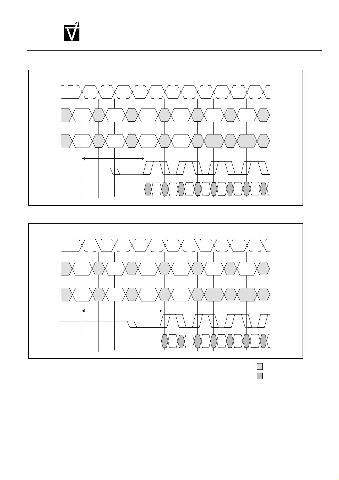
VIS
CLK#
CLK
Preliminary VG37648041AT
256M:x4, x8, x16
CMOS Synchronous Dynamic RAM
COMMAND
ADDRESS
DQS
DQ
CLK#
CLK
COMMAND
READ
Bank,
Col n
READ
CL=2
READ
Bank,
Col x
READ
READ
Bank,
Col b
READ
DO
n
DO
n’
READ
Bank,
Col g
NOP
DO
x
DO
x’
NOP
NOP
b
DO
DO
b’
NOP
NOP
DO
g
ADDRESS
DQS
DQ
Bank,
Col n
Bank,
Col x’
Bank,
Col b
CL=2.5
DO
n
Bank,
Col g
DO
n’
DO
x
DO n, etc.= Data Out from column n, etc.
n’ , etc.=odd or even complement of n, etc. (i.e. column address LSB inverted)
Burst Length=2,4 or 8 in cases shown
Reads are to active rows in any banks
Figure 10a
RANDOM READ ACCESSES - REQUIRED CAS LATENCIES
DO
x’
DO
b
DO
b’
DON’T CARE
UNDEFINED
Document : 1G5-0157 Rev.1 Page 29
Page 30
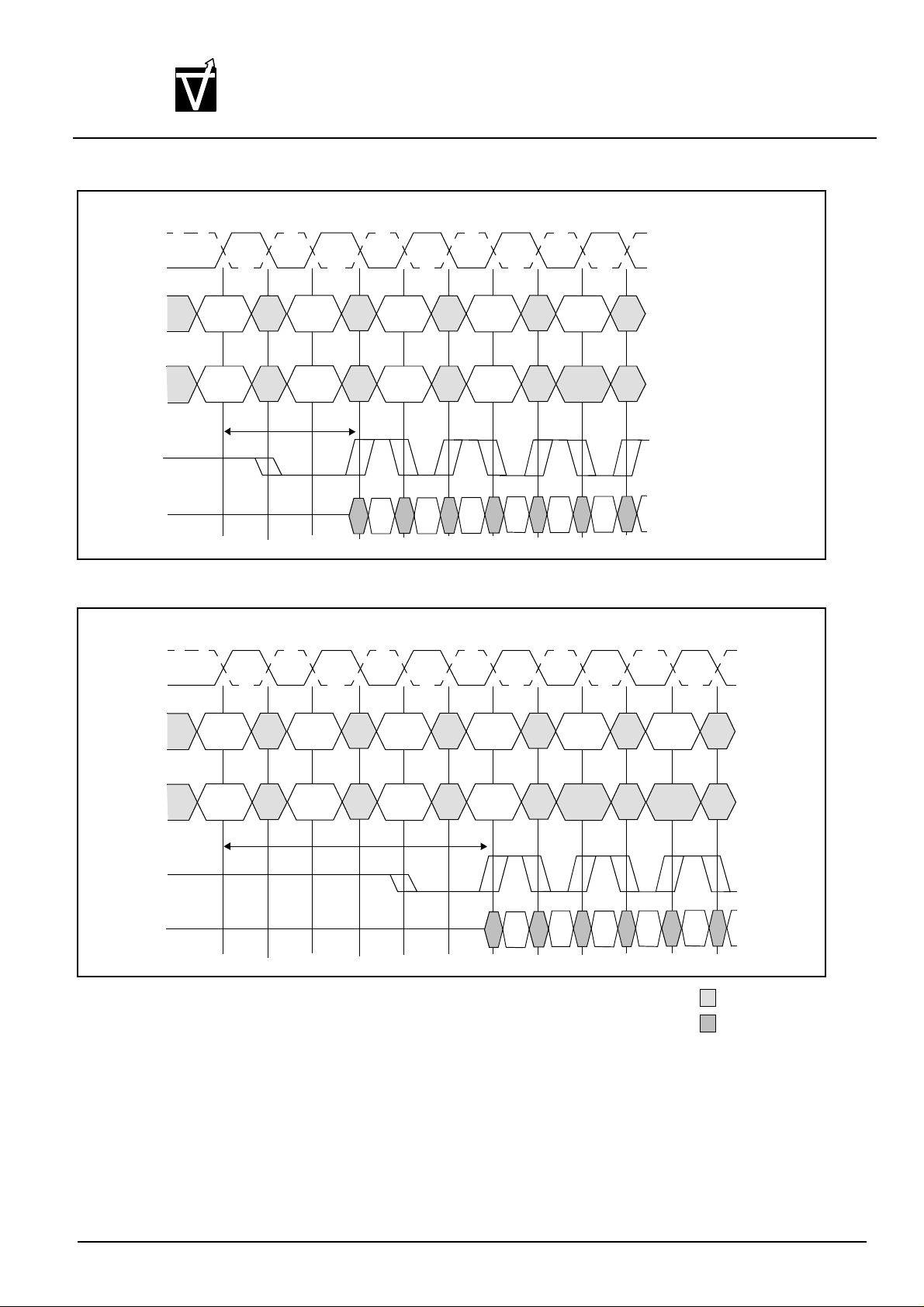
VIS
CLK#
CLK
Preliminary VG37648041AT
256M:x4, x8, x16
CMOS Synchronous Dynamic RAM
COMMAND
ADDRESS
DQS
DQ
CLK#
CLK
COMMAND
READ
Bank,
Col n
READ
CL=1.5
READ
Bank,
Col x
READ
DO
n
READ
Bank,
Col b
READ
DO
n’
DO
x
READ
Bank,
Col g
READ
DO
x’
DO
b
NOP
NOP
DO
b’
NOP
ADDRESS
DQS
DQ
Bank,
Col n
Bank,
Col x
Bank,
Col b
CL=3
Bank,
Col g
DO
n
DO
n’
DO n, etc.= Data Out from column n, etc.
n’ , etc.=odd or even complement of n, etc. (i.e. column address LSB inverted)
Burst Length=2,4 or 8 in cases shown
Reads are to active rows in any banks
Figure 10b
RANDOM READ ACCESSES - OPTIONAL CAS LATENCIES
DO
x
DO
x’
DO
b
DON’T CARE
UNDEFINED
Document : 1G5-0157 Rev.1 Page 30
Page 31

Preliminary VG37648041AT
VIS
256M:x4, x8, x16
CMOS Synchronous Dynamic RAM
Data from any READ burst may be truncated with a BURST TERMINATE command, as shown in Figure 11. The
BURST TERMINATE latency is equal to the read (CAS) latency, i.e. the BURST TERMINATE command should be
issued x cycles after the READ command, where x equals the number of desired data element pairs (pairs are
required by the 2n prefetch architecture).
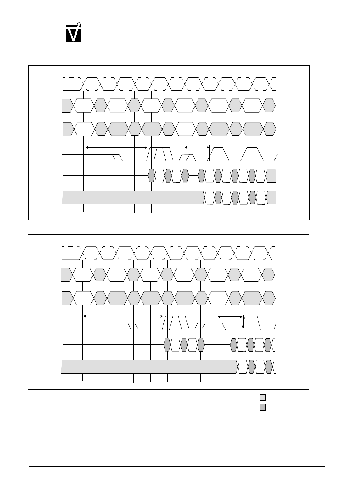
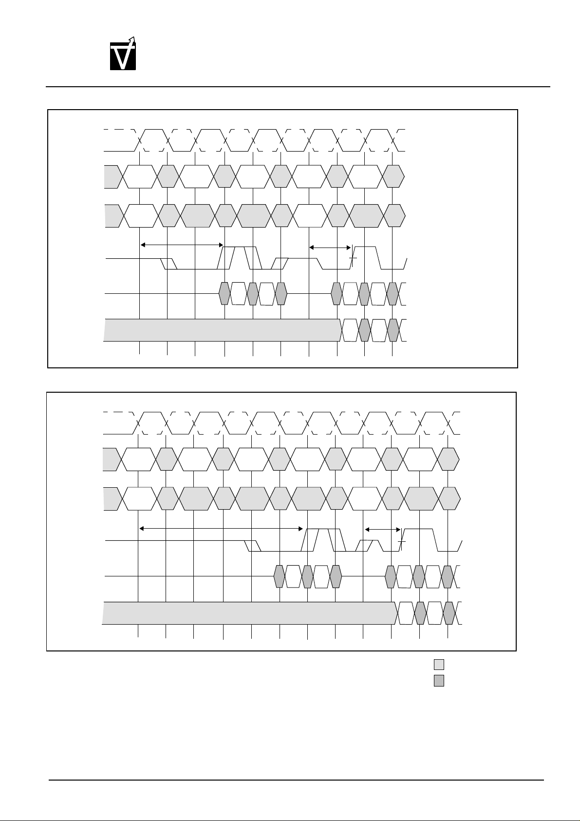
Data from any READ burst must be completed or truncated before a subsequent WRITE command can be
issued. If truncation is necessary, the BURST TERMINATE command must be used, as shown in Figure 12. The
tDDS MIN case is shown; the tDDS MAX case has a longer bus idle time (tDDS MIN and tDDS MAX are defined in
the section on WRITEs).
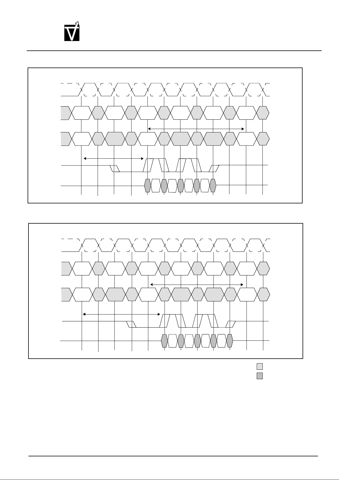
A READ burst may be followed by, or truncated with, a PRECHARGE command to the same bank (provided that
AUTO PRECHARGE was not activated). The PRECHARGE command should be issued x cycles after the READ
command, where x equals the number of desired data element paires (pairs are required by the 2n prefetch architecture). This is shown if Figure 13 for READ latencies of 2.2.5 and 3. Following the PRECHARGE command, a subse-
quent command to the same bank cannot be issued until tRP is met. Note that part of the row precharge time is
hidden during the access of the last data elements.
In the case of a READ being executed to completion. a PRECHARGE command issued at the optimum time
(asdescribed above) provides the same operation that would result from the same READ burst with AUTO PRECHARGE enabled. The disadvantage of the precharge command is that it requires that the command and address
buses be available at the appropriate time to issue the command. The advantage of the PRECHARGE command is
that it can be used to truncate bursts.
Document : 1G5-0157 Rev.1 Page 31
Page 32
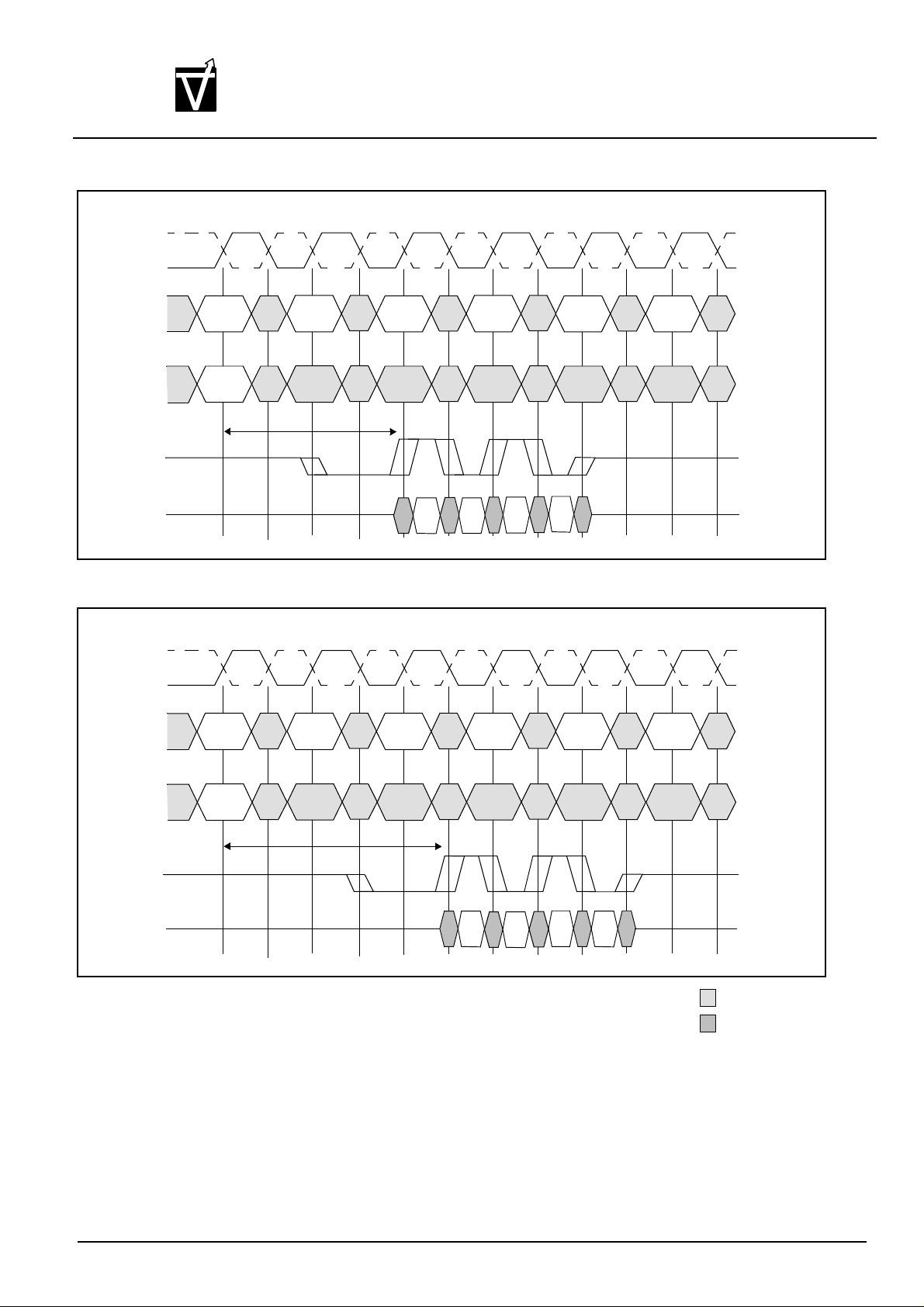
VIS
CLK#
CLK
Preliminary VG37648041AT
256M:x4, x8, x16
CMOS Synchronous Dynamic RAM
COMMAND
ADDRESS
DQS
DQ
CLK#
CLK
COMMAND
READ
Bank a,
Col n
READ
CL=2
NOP
NOP
BST
BST
DO
n
NOP
NOP
NOP
NOP
NOP
NOP
ADDRESS
DQS
DQ
Bank a,
Col n
CL=2.5
DO
n
DO n=Data Out from column n
Cases shown are bursts of 8 terminated after 4 data elements
3 subsequent elements of Data Out appear in the programmed order following DO n
Figure 11a
TERMINATING A READ BURST - REQUIRED CAS LATENCIES
DON’T CARE
UNDEFINED
Document : 1G5-0157 Rev.1 Page 32
Page 33
VIS
CLK#
CLK
Preliminary VG37648041AT
256M:x4, x8, x16
CMOS Synchronous Dynamic RAM
COMMAND
DQS
DQ
CLK#
CLK
COMMAND
READ NOP
CL=1.5
READ
NOP
t
min
NOP
t
AC
max
AC
NOP
NOP
NOP
NOP
NOP
NOP
NOP
ADDRESS
DQS
DQ
Bank a,
Col n
CL=3
DO
n
DO n= Data Out from coulmn n
Burst Length=4
3 subsequent elements of Data Out appear in the programmed order following DO n
Figure 11b
TERMINATING A READ BURST - OPTIONAL CAS LATENCIES
DON’T CARE
UNDEFINED
Document : 1G5-0157 Rev.1 Page 33
Page 34
VIS
CLK#
CLK
Preliminary VG37648041AT
256M:x4, x8, x16
CMOS Synchronous Dynamic RAM
COMMAND
ADDRESS
DQS
DQ
DM
CLK#
CLK
READ
Bank,
Col n
CL=2
BST
NOP
DO
n
DO
n’
WRITE
Bank,
Col b
t
DSS
min
NOP
D1
b
NOP
COMMAND
ADDRESS
DQS
DQ
DM
DO n(or b)=Data Out from column n (or column b)
READ
Bank,
Col n
BST
CL=2.5
NOP
DO
n
NOP
n’
DO
WRITE
Bank,
Col b
t
DSS
min
NOP
D1
b
DON’T CARE
UNDEFINED
Burst Length= 4 in the cases shown (applies for bursts of 8 as well; if burst length is 2,
the BST command shown can be NOP)
3 subsequent elements of Data Out appear in the programmed order following DO n (and following DO b)
Figure 12a
READ TO WRITE - REQUIRED CAS LATENCIES
Document : 1G5-0157 Rev.1 Page 34
Page 35
VIS
CLK#
CLK
Preliminary VG37648041AT
256M:x4, x8, x16
CMOS Synchronous Dynamic RAM
COMMAND
ADDRESS
DQS
DQ
DM
CLK#
CLK
READ
Bank,
Col n
CL=1.5
BST
DO
n
NOP
DO
n’
WRITE
Bank,
Col b
t
DSS
min
NOP
D1
b
COMMAND
ADDRESS
DQS
DQ
DM
DO n(or b)=Data Out column n (or column b)
READ
Bank,
Col n
BST
CL=3
NOP
DO
n
NOP
n’
DO
WRITE
Bank,
Col b
t
DSS
min
NOP
D1
b
DON’T CARE
UNDEFINED
Burst Length= 4 in the cases shown (applies for bursts of 8 as well; if burst length is 2,
the BST command shown can be NOP)
3 subsequent elements of Data Out appear in the programmed order following DO n (and following DO b)
Figure 12b
READ TO WRITE -OPTIONAL CAS LATENCIES
Document : 1G5-0157 Rev.1 Page 35
Page 36
VIS
CLK#
CLK
Preliminary VG37648041AT
256M:x4, x8, x16
CMOS Synchronous Dynamic RAM
COMMAND
ADDRESS
DQS
DQ
CLK#
CLK
COMMAND
READ
Bank a,
Col n
READ
NOP
NOP
CL=2
PRE
Bank
(a or all)
PRE
DO
n
NOP
NOP
NOP
t
RP
NOP
ACT
Bank a,
Row
ACT
t
RP
ADDRESS
DQS
DQ
Bank a,
Col n
CL=2.5
Bank a,
(a or all)
DO
n
DO n=Data Out from column n
Cases shown are either uninterrupted bursts of 4, or interrupted bursts of 8
3 subsequent elements of Data Out appear in the programmed order following DO n
Figure 13a
READ TO PRECHARGE - REQUIRED CAS LATENCIES
Bank a,
Row
DON’T CARE
UNDEFINED
Document : 1G5-0157 Rev.1 Page 36
Page 37
VIS
CLK#
CLK
Preliminary VG37648041AT
256M:x4, x8, x16
CMOS Synchronous Dynamic RAM
COMMAND
ADDRESS
DQS
DQ DO
CLK#
CLK
COMMAND
READ
Bank a,
Col n
READ
NOP
CL=1.5
NOP
n
PRE
Bank
(a or all)
PRE
NOP
NOP
NOP
t
RP
NOP
ACT
Bank a,
Row
ACT
t
RP
ADDRESS
DQS
DQ
Bank a,
Col n
CL=3
Bank
(a or all)
DO
n
DO n=Data Out from column n
Cases shown are either uninterrupted bursts of 4, or interrupted bursts of 8
3 subsequent elements of Data Out appear in the programmed order following DO n
Figure 13b
READ TO PRECHARGE - OPTIONAL CAS LATENCIES
Bank a,
Row
DON’T CARE
UNDEFINED
Document : 1G5-0157 Rev.1 Page 37
Page 38

Preliminary VG37648041AT
VIS
256M:x4, x8, x16
CMOS Synchronous Dynamic RAM
WRITEs
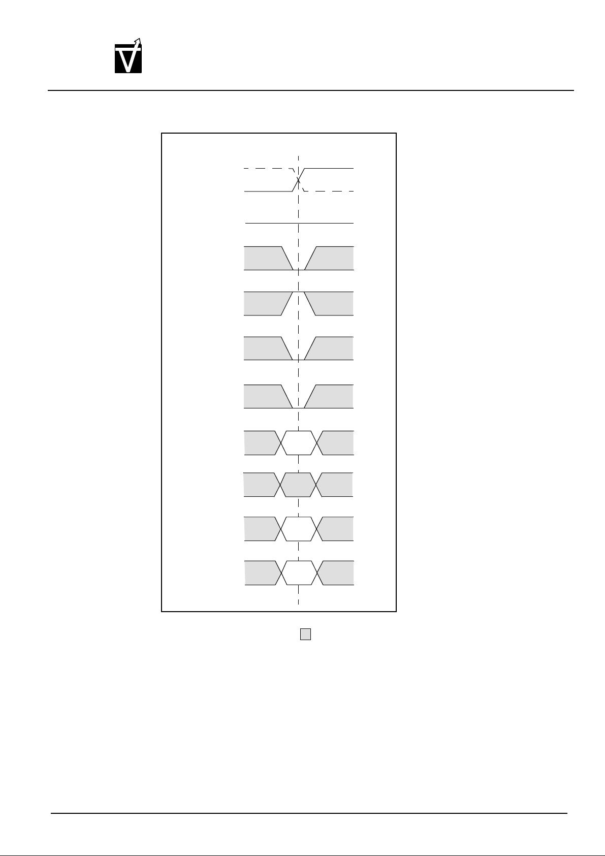
WRITE bursts are initiated with a WRITE command, as shown in figure 14.
The starting column and bank addresses are provided with the WRITE command, and AUTO PRECHARGE
is either enabled or disabled for that acess. If AUTOPRECHARGE is enabled, the row being accessed is precharged at the completion of the burst. For the generic WRITE commands used in the following illustrations,
AUTOPRECHARGE is disabled.
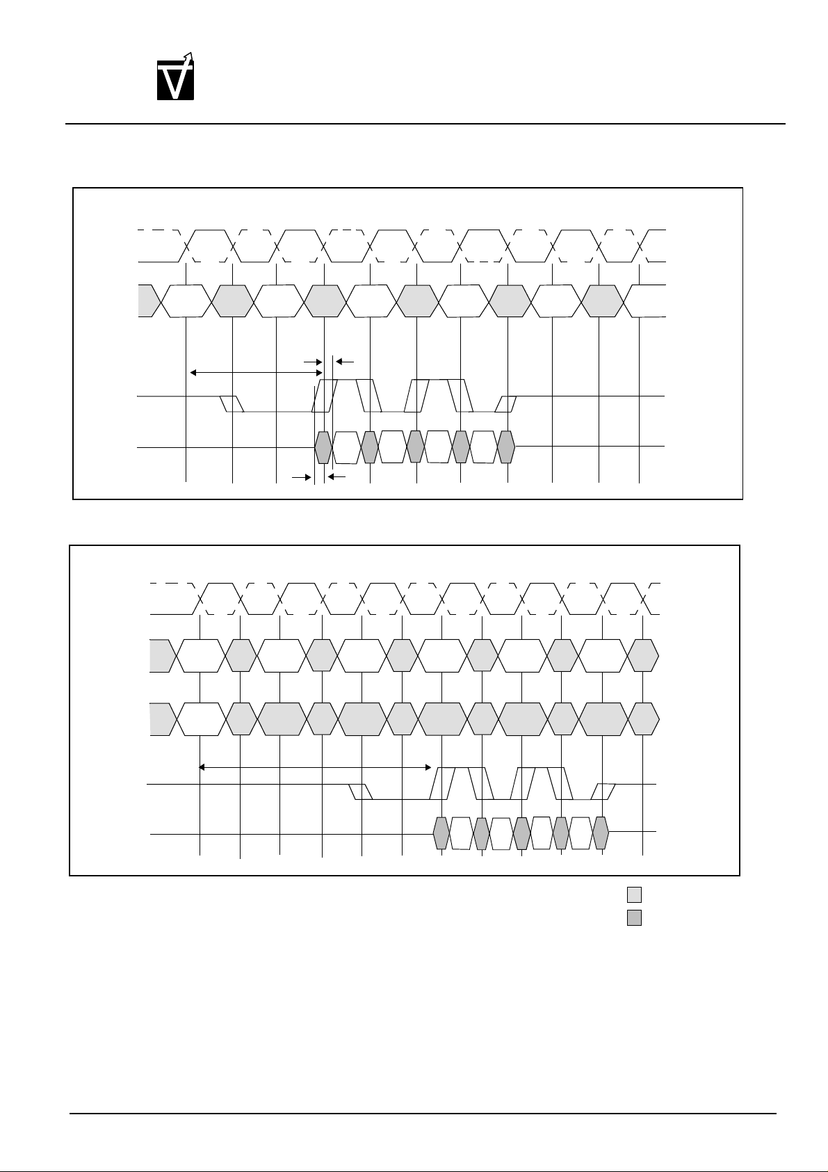
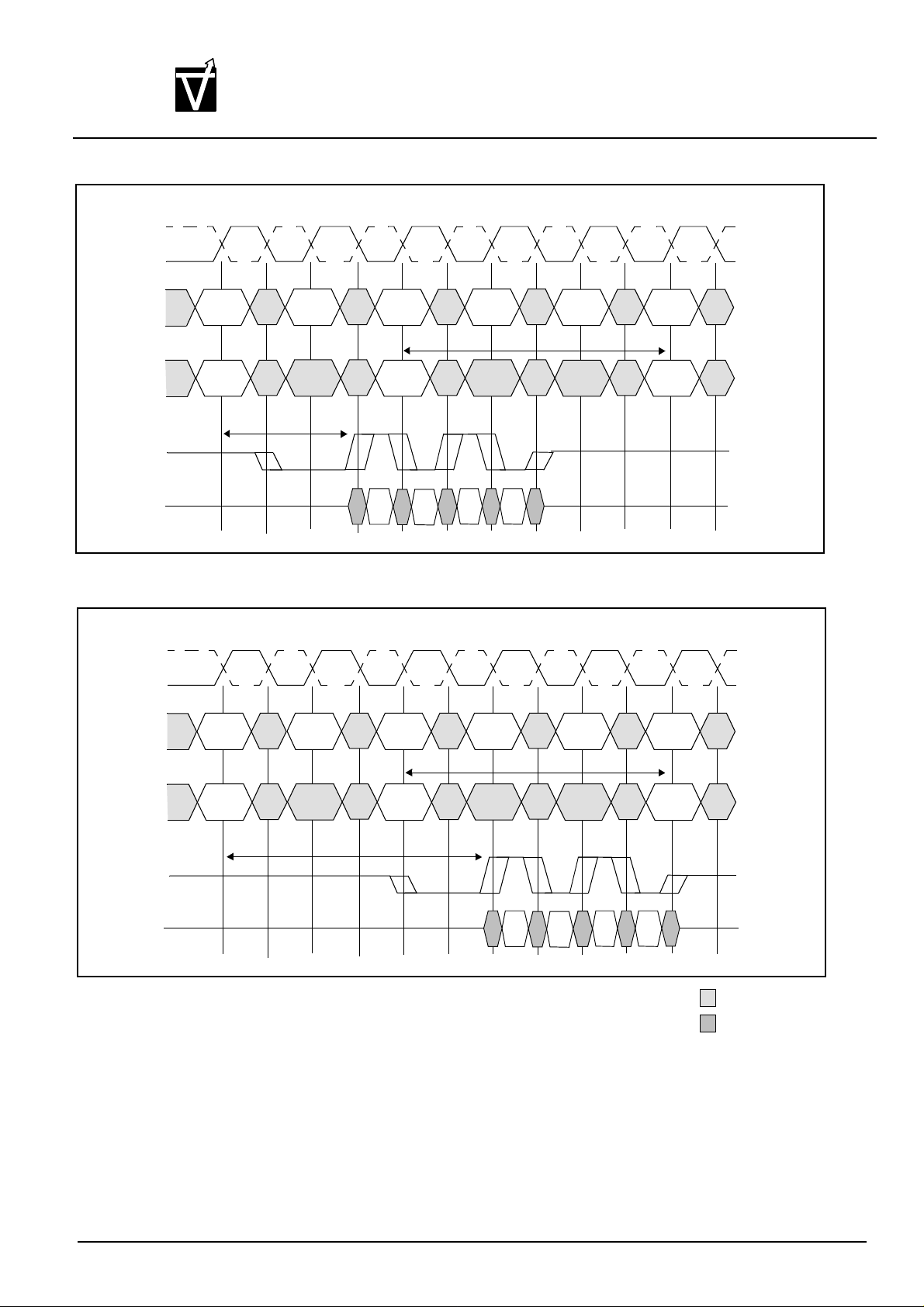
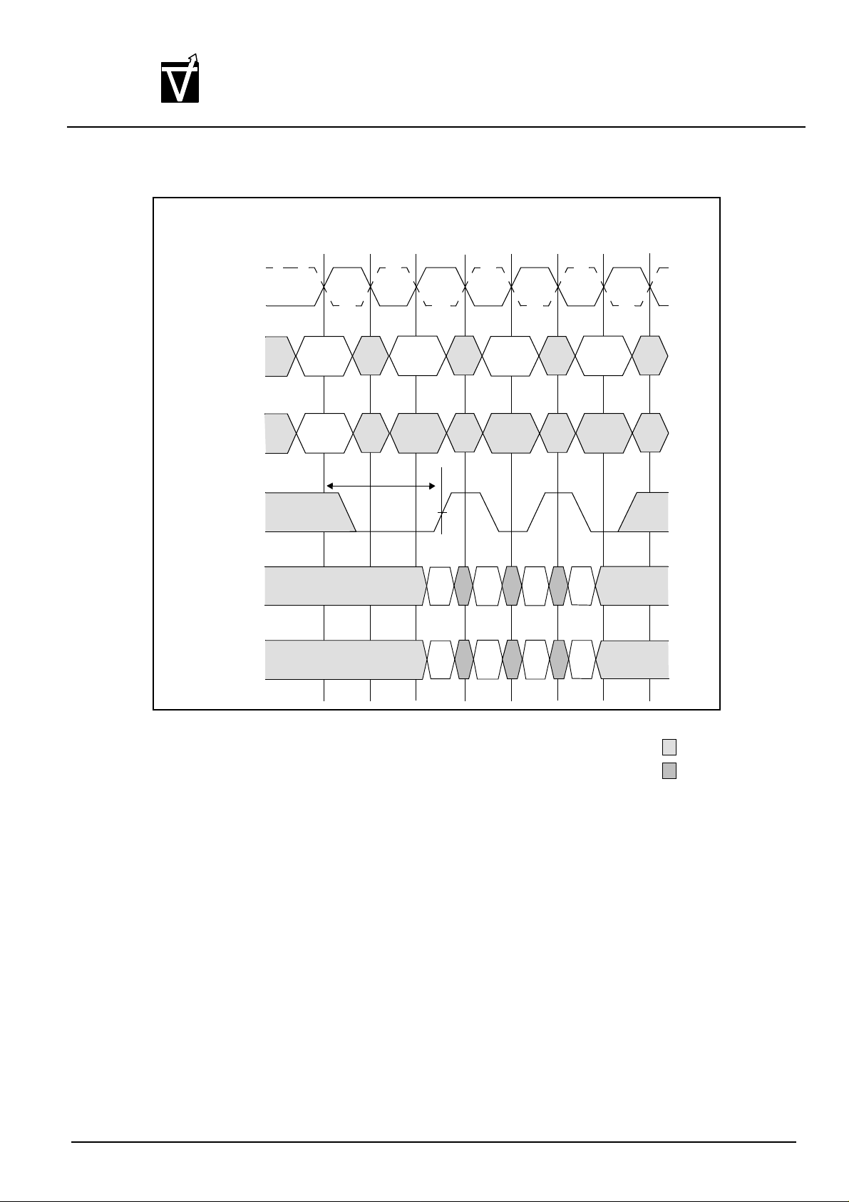
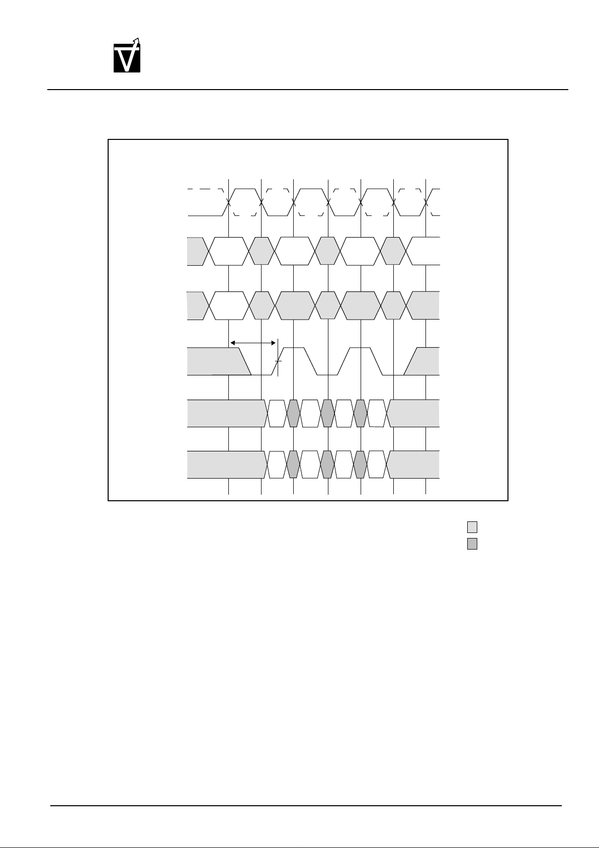
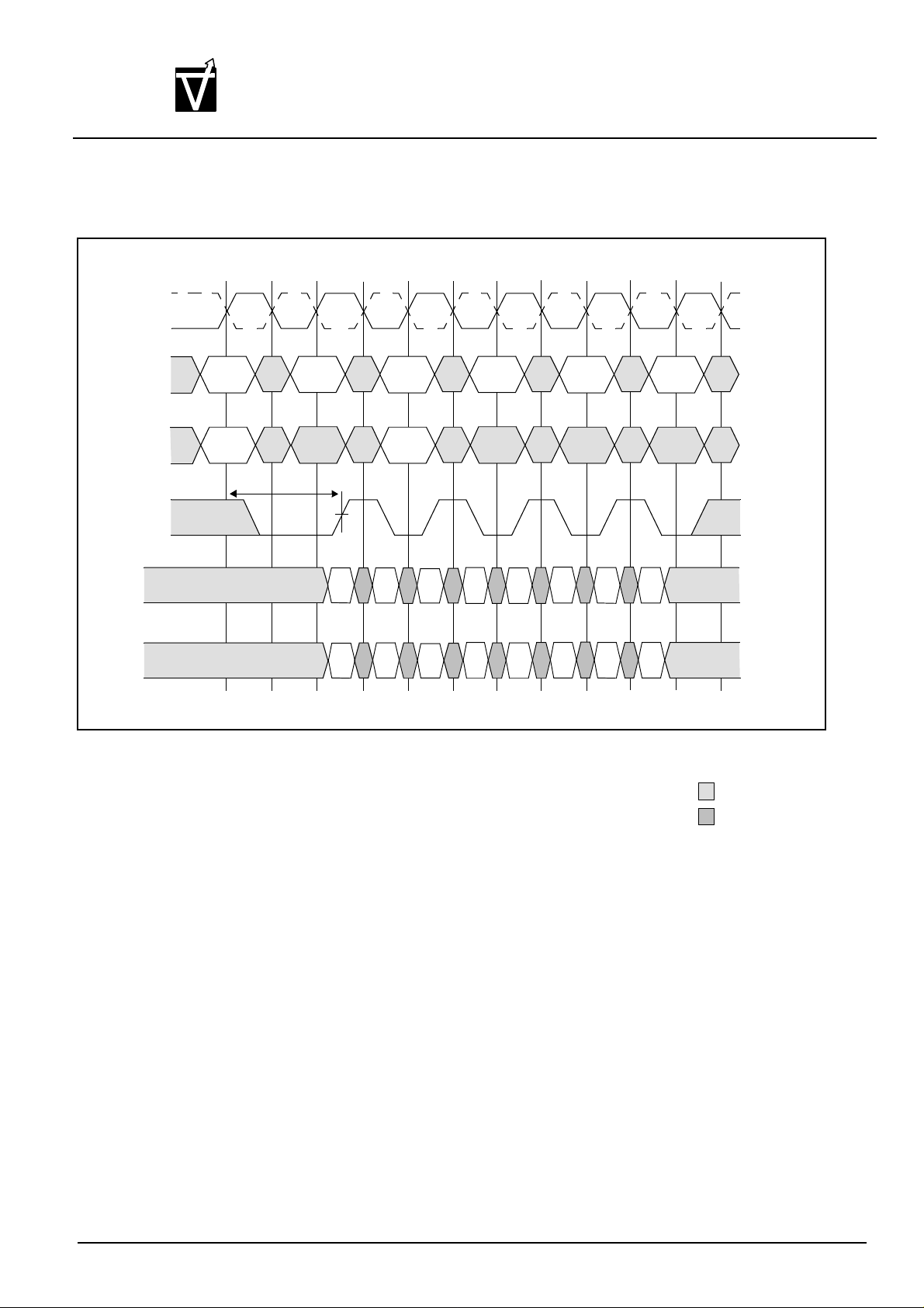
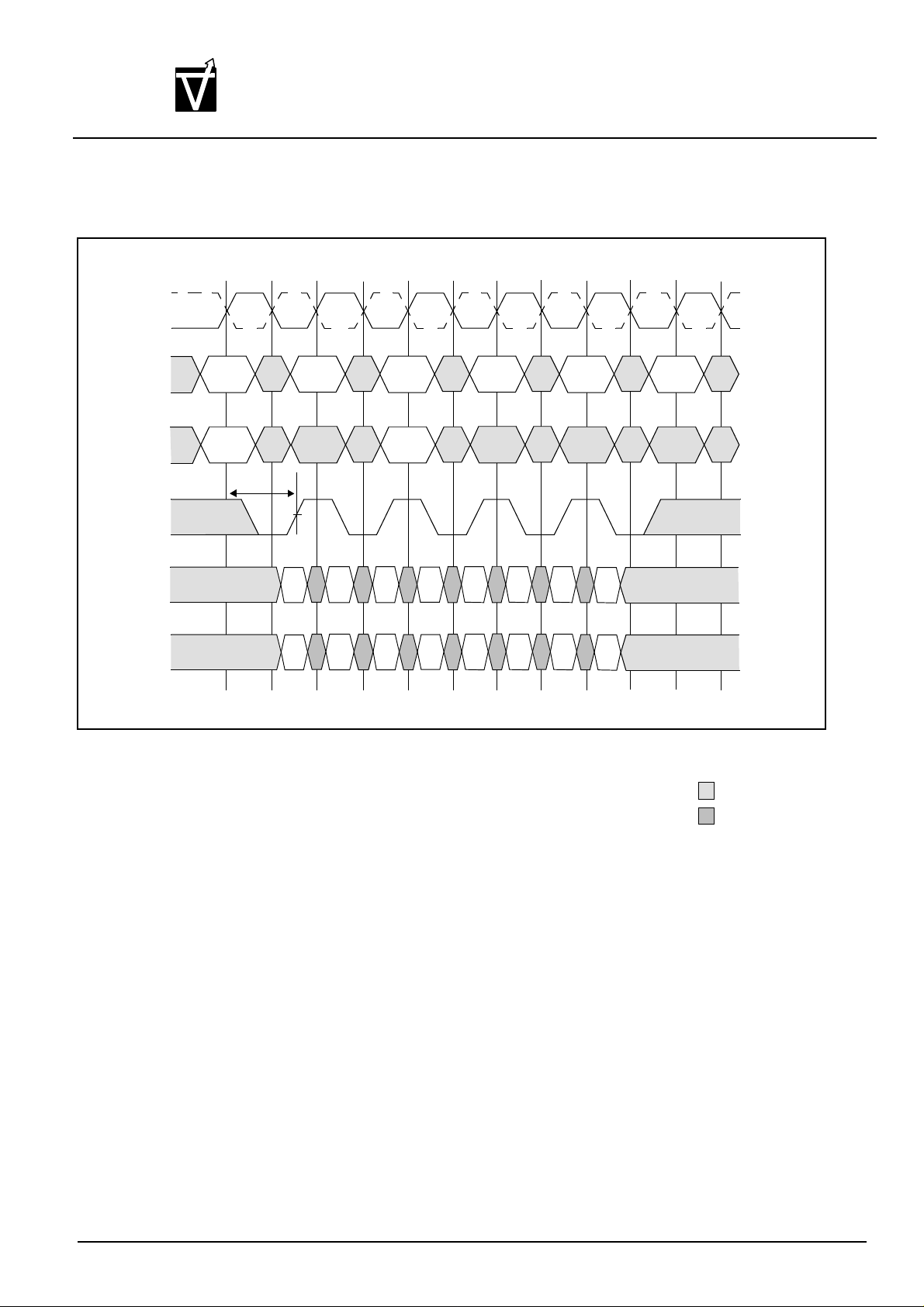
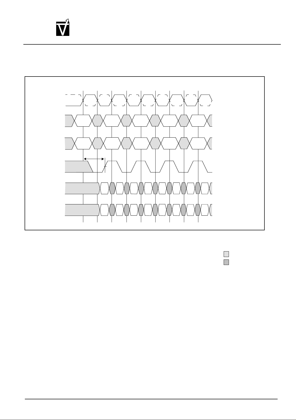
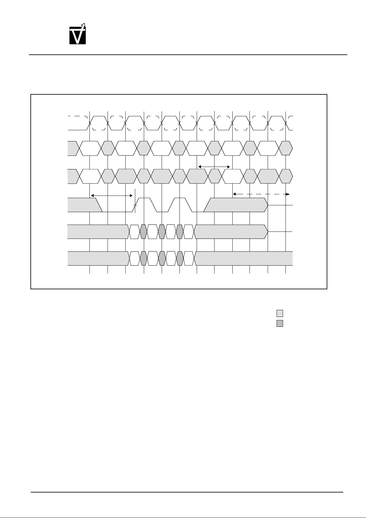
During WRITE bursts, the first valid data-in element will be registered on the first rising edge of DQS following the write command, and subsequent data elements will be registered on successive edges of DQS. The
LOW state on DQS between the WRITE command and the first rising edge is known as the write preamble; the
LOW state on DQS following the last data-in element is known as the write postamble. The time between the
WRITE command and the first corresponding rising edge of DQS (tDSS) is specified with a relatively wide range
(from 75% to 125% of 1 clock cycle), so most of the WRITE diagrams that follow are drawn for the two extreme
cases (i.e. tDSS MIN and tDSS MAX). Figures 15 and 16 show the two extremes of tDSS for a burst of 4. Upon
completion of a burst, assuming no other commands have been initiated, the DQs will remain High-Z and any
additional input data will be ignored.
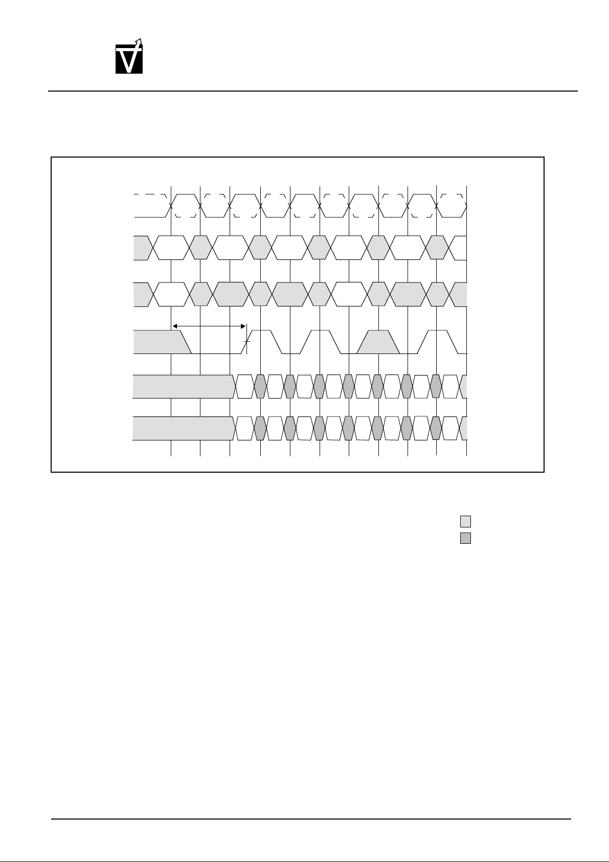
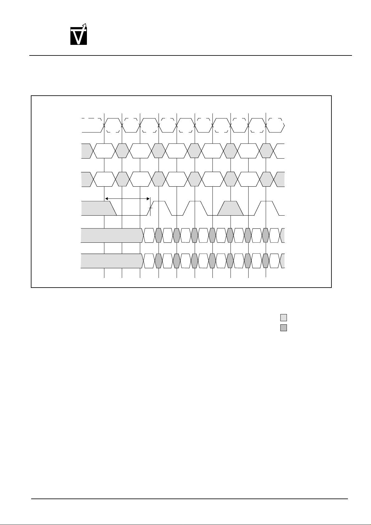
Data for any WRITE burst may be concatenated with or truncated with a subsequent WRITE command. In
either case, a continuous flow of input data can be maintained. The new WRITE command can be issued on any
clock following the previous WRITE command. The first data element from the new burst is applied after either
the last element of a completed burst or the last desired data element of a longer burst which is being truncated.
The new WRITE command should be issued x cycles after the first WRITE command, where x equals the
number of desired data element pairs (pairs are required by the 2n prefetch architecture). Figures 17 and 18
show concatenated bursts of 4. An example of non-consecutive WRITEs is shown in Figure 19. Full-speed random write accesses within a page or pages can be performed as shown in Figures 20 and 21.
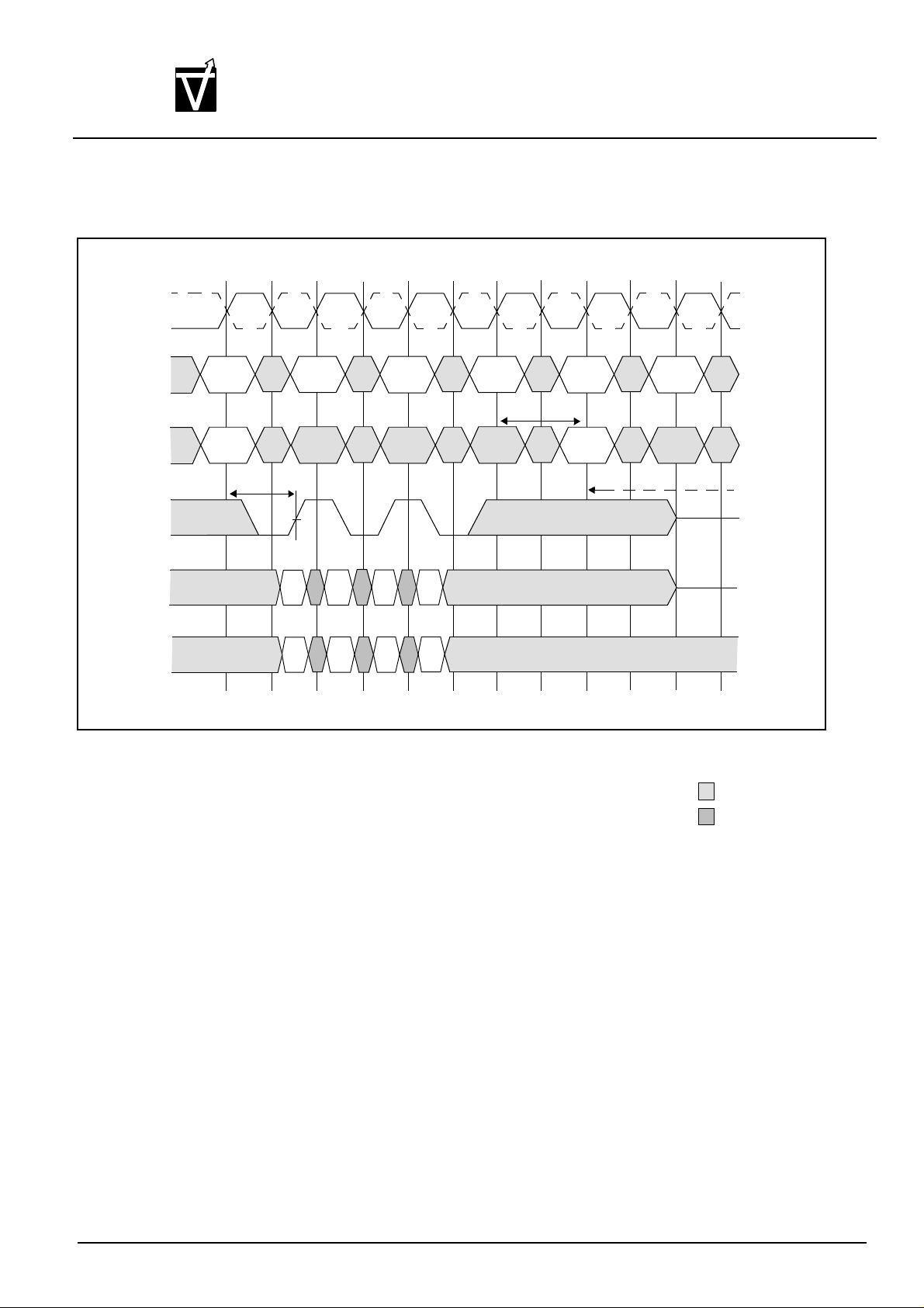
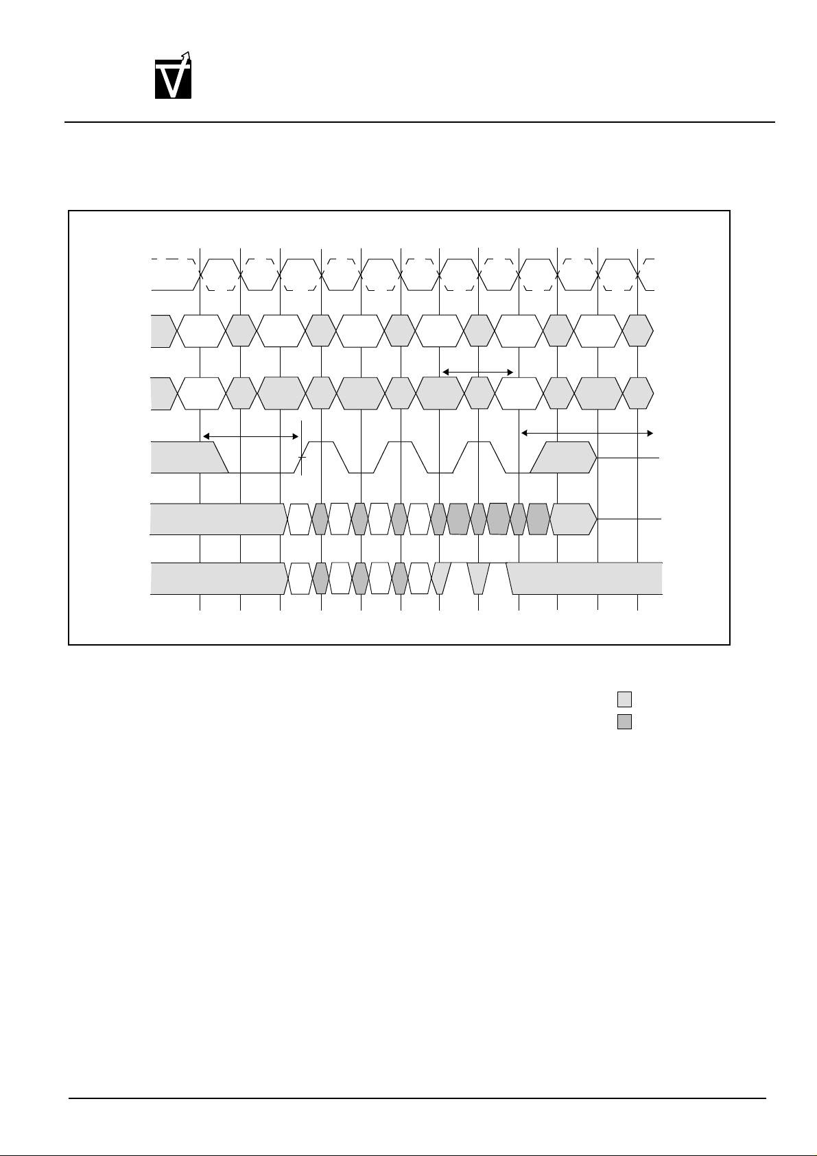
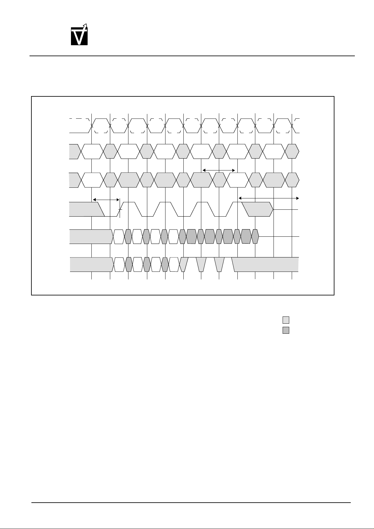
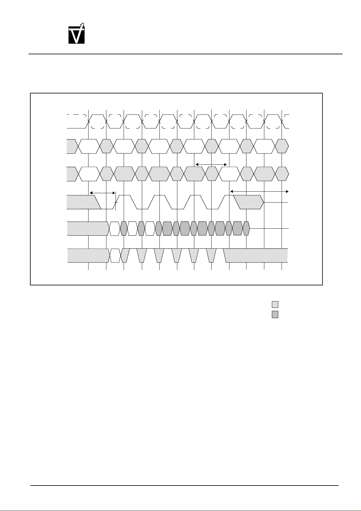
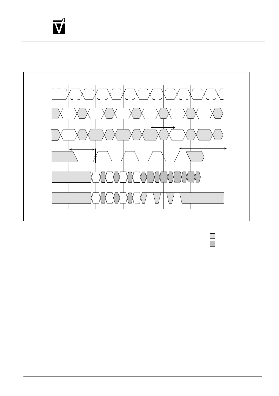
Data for any WRITE burst may be followed by a subsequent READ command. To follow a WRITE without
truncating the write burst, tWTR should be met as shown in Figures 22 and 23.
Data for any WRITE burst may be truncated by a subsequent READ command, as shown in Figures 24-27.
Note that only the data-in pairs that are registered prior to the tWTR period are written to the internal array, and
any subsequent data-in should be masked with DM(through one-half clock after the READ command).
Document : 1G5-0157 Rev.1 Page 38
Page 39
VIS
Preliminary VG37648041AT
256M:x4, x8, x16
CMOS Synchronous Dynamic RAM
CLK#
CLK
CKE
HIGH
CS#
RAS#
CAS#
WE#
x4:A0-A11
x8:A0-A9
x16:A0-A8
x4:A12
x8:A9,A12
x16:A8,A9,A12
A10
BA0,1
CA
EN AP
DIS AP
BA
=DON’T CARE
CA = Column Address
BA = Bank Address
EN AP = Enable Autoprecharge
DIS AP = Disable Autoprecharge
Figure 14
WRITE COMMAND
Document : 1G5-0157 Rev.1 Page 39
Page 40
VIS
Preliminary VG37648041AT
256M:x4, x8, x16
CMOS Synchronous Dynamic RAM
CLK#
CLK
COMMAND
ADDRESS
DQS
DQ
T0
WRITE
Bank a,
Col b
T1 T2 T3 T4 T5
t
DSS
NOP
max
Dl
b
NOP
T6
NOP
T7
DM
Dl b=Data In for column b
3 subsequent elements of Data In are applied in the programmed order following Dl b
A non-interrupted burst of 4 is shown
A10 is LOW with the WRITE command (AUTO PRECHARGE is disabled)
Figure 15
WRITE BURST - MAX DSS
DON’T CARE
UNDEFINED
Document : 1G5-0157 Rev.1 Page 40
Page 41
VIS
Preliminary VG37648041AT
256M:x4, x8, x16
CMOS Synchronous Dynamic RAM
CLK#
CLK
COMMAND
ADDRESS
DQS
DQ
T0
WRITE
Bank a,
Col b
T1 T2 T3 T4 T5
t
DSS
min
NOP
Dl
b
NOP
T6
NOP
DM
Dl b=Data In for column b
3 subsequent elements of Data In are applied in the programmed order following Dl b
A non-interrupted burst of 4 is shown
A10 is LOW with the WRITE command (AUTO PRECHARGE is disabled)
Figure 16
WRITE BURST - MIN DSS
DON’T CARE
UNDEFINED
Document : 1G5-0157 Rev.1 Page 41
Page 42

Preliminary VG37648041AT
VIS
256M:x4, x8, x16
CMOS Synchronous Dynamic RAM
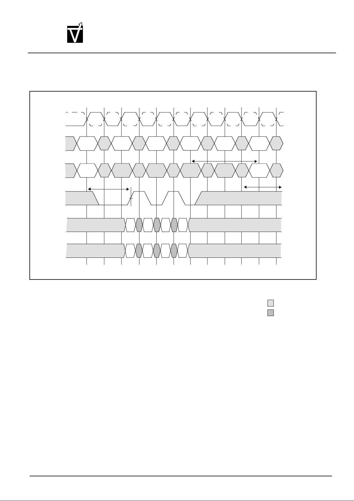
Data for any WRITE burst may be followed by a subsequent PRECHARGE command. To follow a WRITE with
out truncating the write burst, tWR should be met as shown in Figures 28 and 29.
Data for any WRITE burst may be truncated by a subsequent PRECHARGE command, as shown in Figures
30-33. Note that only the data -in pairs that are registered prior to the tWR period are written to the internal array,
and any subsequent data-in should be masked with DM (through one-half clock after the READ command). Following the PRECHARGE command, a subsequent command to the same bank can not be issued until tRP is
met.
In the case of a write burst being executed to completion, a PRECHARGE command issued at the optimum
time (as described above) provides the same operation that would result from the same burst with AUTO PRECHARGE. The disadvantage of the PRECHARGE command is that it requires that the command and address
buses be available at the appropriate time to issue the command. The advantage of the PRECHARGE command
is that it can be used to truncate bursts.
Document : 1G5-0157 Rev.1 Page 42
Page 43
VIS
Preliminary VG37648041AT
256M:x4, x8, x16
CMOS Synchronous Dynamic RAM
CLK#
CLK
COMMAND
ADDRESS
DQS
DQ
DM
T0 T1
WRITE
Bank,
Col b
T2 T3 T4 T5 T6 T7
t
max
DSS
NOP
Dl
b
WRITE
Bank,
Col n
NOP
T9
T8
NOP
Dl
n
T10
NOP
T11
Dl b, etc. = Data In for column b, etc.
3 subsequent elements of Data In are applied in the programmed order following Dl b
3 subsequent elements of Data In are applied in the programmed order following Dl n
A non-interrupted burst of 4 is shown
Each Write command may be to any bank
Figure 17
WRITE TO WRITE - MAX DSS
DON’T CARE
UNDEFINED
Document : 1G5-0157 Rev.1 Page 43
Page 44
VIS
Preliminary VG37648041AT
256M:x4, x8, x16
CMOS Synchronous Dynamic RAM
CLK#
CLK
COMMAND
ADDRESS
DQS
DQ
DM
T0 T1
WRITE
Bank,
Col b
t
DSS
min
T2 T3 T4 T5 T6 T7
NOP
Dl
b
WRITE
Bank,
Col n
Dl
n
NOP
T8
NOP
T9
T10
NOP
T11
Dl b, etc. = Data In for column b, etc.
3 subsequent elements of Data In are applied in the programmed order following Dl b
3 subsequent elements of Data In are applied in the programmed order following Dl n
A non-interrupted burst of 4 is shown
Each Write command may be to any bank
Figure 18
WRITE TO WRITE - MIN DSS
DON’T CARE
UNDEFINED
Document : 1G5-0157 Rev.1 Page 44
Page 45
VIS
Preliminary VG37648041AT
256M:x4, x8, x16
CMOS Synchronous Dynamic RAM
CLK#
CLK
COMMAND
ADDRESS
DQS
DQ
DM
T0 T1
WRITE
Bank,
Col b
t
max
DSS
T2
NOP
T3
T4 T5 T6 T7
NOP
Dl
b
WRITE
Bank,
Col n
T8
NOP
Dl
n
T10
T9
Dl b, etc. = Data In for column b, etc.
3 subsequent elements of Data In are applied in the programmed order following Dl b
3 subsequent elements of Data In are applied in the programmed order following Dl n
A non-iterrupted burst of 4 is shown
Each Write command may be to any bank
Figure 19
WRITE TO WRITE - MAX DSS, NON-CONSECUTIVE
DON’T CARE
UNDEFINED
Document : 1G5-0157 Rev.1 Page 45
Page 46
VIS
Preliminary VG37648041AT
256M:x4, x8, x16
CMOS Synchronous Dynamic RAM
CLK#
CLK
COMMAND
ADDRESS
DQS
DQ
DM
T0 T1
WRITE
Bank,
Col b
t
max
DSS
T2
WRITE
Bank,
Col x
T3
T4 T5 T6 T7
Dl
n’
WRITE
Bank,
Col g
WRITE
Bank,
Col n
Dl
b
b’
Dl
Dl
x
Dl
x’
WRITE
Bank,
Col a
Dl
n
T9
T8
Dl
Dl
a’
a
Dl b, etc.=Data In for coulmn b, etc.
b’,etc.=odd or even complement of b, etc.(i.e. column address LSB inverted)
Programmed burst Length=2,4 or 8 in cases shown
Each Write command may be to any bank.
Figure 20
RANDOM WRITE CYCLES - MAX DSS
DON’T CARE
UNDEFINED
Document : 1G5-0157 Rev.1 Page 46
Page 47
VIS
Preliminary VG37648041AT
256M:x4, x8, x16
CMOS Synchronous Dynamic RAM
CLK#
CLK
COMMAND
ADDRESS
DQS
DQ
DM
T0 T1
WRITE
Bank,
Col b
t
DSS
min
Dl
b
T2
WRITE
Bank,
Col x
T3
T4 T5 T6 T7
WRITE
Bank,
Col n
Dl
Dl
Dl
b’
x’
x
Dl
n
WRITE
Bank,
Col a
Dl
n’
Dl
a
T8
WRITE
Bank,
Col g
Dl
a’
Dl b, etc.=Data In for coulmn b, etc.
b’,etc.=odd or even complement of b, etc.(i.e. column address LSB inverted)
Programmed burst Length=2,4 or 8 in cases shown
Each Write command may be to any bank.
Figure 21
RANDOM WRITE CYCLES - MIN DSS
DON’T CARE
UNDEFINED
Document : 1G5-0157 Rev.1 Page 47
Page 48
VIS
Preliminary VG37648041AT
256M:x4, x8, x16
CMOS Synchronous Dynamic RAM
CLK#
CLK
COMMAND
ADDRESS
DQS
DQ
DM
T0 T1
WRITE
Bank,
Col b
T2 T3 T4 T5 T6 T7
t
DSS
max
NOP
Dl
b
NOP
NOP
t
WTR
T8
READ
Bank,
Col n
T9
T10
NOP
CL
T11
Dl b=Data In for column b
3 subsequent elements of Data In are applied in the programmed order following Dl b
A non-interrupted burst of 4 is shown
t
is referenced from the first positive CLK edge after the last Data In pair
WTR
A10 is LOW with the WRITE command (AUTO PRECHARGE is disabled)
The READ and WRITE commands are not necessarily to the same bank
Figure 22
WRITE TO READ - MAX DSS, NON-INTERRUPTING
DON’T CARE
UNDEFINED
Document : 1G5-0157 Rev.1 Page 48
Page 49
VIS
Preliminary VG37648041AT
256M:x4, x8, x16
CMOS Synchronous Dynamic RAM
CLK#
CLK
COMMAND
ADDRESS
DQS
DQ
DM
T0 T1
WRITE
Bank,
Col b
t
DSS
min
T2 T3 T4 T5 T6 T7
NOP
Dl
b
NOP
NOP
t
WTR
T8
READ
Bank,
Col n
T9
T10
NOP
CL
T11
Dl b=Data In for column b
3 subsequent elements of Data In are applied in the programmed order following Dl b
A non-interrupted burst of 4 is shown
t
is referenced from the first positive CLK edge after the last Data In pair
WTR
A10 is LOW with the WRITE command (AUTO PRECHARGE is disabled)
The READ and WRITE commands are not necessarily to the same bank
Figure 23
WRITE TO READ - MIN DSS, NON-INTERRUPTING
DON’T CARE
UNDEFINED
Document : 1G5-0157 Rev.1 Page 49
Page 50
VIS
Preliminary VG37648041AT
256M:x4, x8, x16
CMOS Synchronous Dynamic RAM
CLK#
CLK
COMMAND
ADDRESS
DQS
DQ
DM
T0 T1
WRITE
Bank,
Col b
T2 T3 T4 T5 T6 T7
t
DSS
max
NOP
Dl
b
NOP
NOP
t
WTR
T8
READ
Bank,
Col n
T9
T10
NOP
CL
T11
Dl b=Data In for column b
An interrupted burst of 8 is shown, 4 data elements are written
3 subsequent elements of Data In are applied in the programmed order following Dl b
t
is referenced from the first positive CLK edge after the last Data In pair
WTR
A10 is LOW with the WRITE command (AUTO PRECHARGE is disabled)
The READ and WRITE commands are not necessarily to the same bank
Figure 24
WRITE TO READ - MAX DSS, INTERRUPTING
DON’T CARE
UNDEFINED
Document : 1G5-0157 Rev.1 Page 50
Page 51
VIS
Preliminary VG37648041AT
256M:x4, x8, x16
CMOS Synchronous Dynamic RAM
CLK#
CLK
COMMAND
ADDRESS
DQS
DQ
DM
T0 T1
WRITE
Bank,
Col b
t
DSS
min
T2 T3 T4 T5 T6 T7
NOP
Dl
b
NOP
NOP
t
WTR
T8
READ
Bank,
Col n
T9
T10
NOP
CL
T11
Dl b=Data In for column b
An interrupted burst of 8 is shown, 4 data elements are written
3 subsequent elements of Data In are applied in the programmed order following Dl b
t
is referenced from the first positive CLK edge after the last desired Data In pair
WTR
A10 is LOW with the WRITE command (AUTO PRECHARGE is disabled)
The READ and WRITE commands are not necessarily to the same bank
Figure 25
WRITE TO READ - MIN DSS, INTERRUPTING
DON’T CARE
UNDEFINED
Document : 1G5-0157 Rev.1 Page 51
Page 52
VIS
Preliminary VG37648041AT
256M:x4, x8, x16
CMOS Synchronous Dynamic RAM
CLK#
CLK
COMMAND
ADDRESS
DQS
DQ
DM
T0 T1
WRITE
Bank,
Col b
t
DSS
min
T2 T3 T4 T5 T6 T7
NOP
Dl
b
NOP
NOP
t
WTR
T8
READ
Bank,
Col n
T9
T10
NOP
CL
T11
Dl b= Data In for column b
An interrupted burst of 8 is shown, 3 data elements are written
2 subsequent elements of Data In are applied in the programmed order following Dl b
t
is referenced from the first positive CLK edge after the last desired Data in pair (not the last desired
WTR
data in element)
A10 is LOW with the WRITE command (AUTO PRECHARGE is disabled)
The READ and WRITE commands are not necessarily to the same bank
Figure 26
WRITE TO READ - MIN DSS, ODD NUMBER OF DATA, INTERRUPTING
DON’T CARE
UNDEFINED
Document : 1G5-0157 Rev.1 Page 52
Page 53
VIS
Preliminary VG37648041AT
256M:x4, x8, x16
CMOS Synchronous Dynamic RAM
CLK#
CLK
COMMAND
ADDRESS
DQS
DQ
DM
T0 T1
WRITE
Bank,
Col b
t
DSS
nom
T2 T3 T4 T5 T6 T7
NOP
Dl
b
NOP
NOP
t
WTR
T8
READ
Bank,
Col n
CL
T10
NOP
T11
T9
Dl b= Data In for column b
An interrupted burst of 8 is shown, 4 data elements are written
3 subsequent elements of Data In are applied in the programmed order following Dl b
t
is referenced from the first positive CLK edge after the last desired Data In pair
WTR
A10 is LOW with the WRITE command (AUTO PRECHARGE is disabled)
The READ and WRITE commands are not necessarily to the same bank
Figure 27
WRITE TO READ - NOMINAL DSS, INTERRUPTING
DON’T CARE
UNDEFINED
Document : 1G5-0157 Rev.1 Page 53
Page 54
VIS
Preliminary VG37648041AT
256M:x4, x8, x16
CMOS Synchronous Dynamic RAM
CLK#
CLK
COMMAND
ADDRESS
DQS
DQ
DM
T0 T1
WRITE
Bank a,
Col b
T2 T3 T4 T5 T6 T7
t
DSS
max
NOP
Dl
b
NOP
NOP
T9
T8
NOP
t
WR
T10
PRE
Bank,
(a or all)
t
T11
RP
Dl b=Data In for column b
3 subsequent elements of Data In are applied in the programmed order following Dl b
A non-interrupted burst of 4 is shown
t
is referenced from the first positive CLK edge after the last Data In pair
WTR
A10 is LOW with the WRITE command (AUTO PRECHARGE is disabled)
Figure 28
WRITE TO PRECHARGE - MAX DSS, NON-INTERRUPTING
DON’T CARE
UNDEFINED
Document : 1G5-0157 Rev.1 Page 54
Page 55
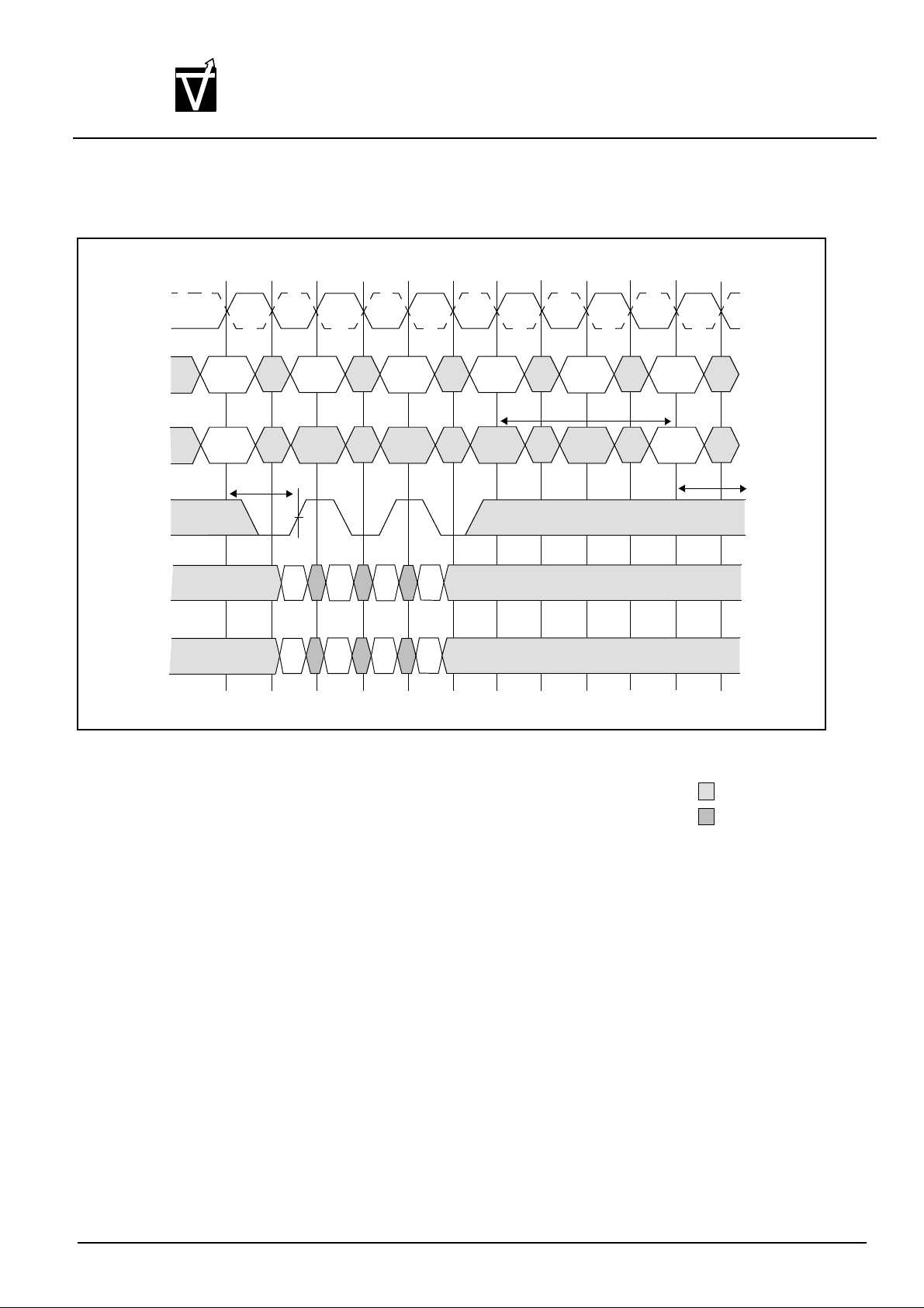
VIS
Preliminary VG37648041AT
256M:x4, x8, x16
CMOS Synchronous Dynamic RAM
CLK#
CLK
COMMAND
ADDRESS
DQS
DQ
DM
T0 T1
WRITE
Bank a,
Col b
t
DSS
min
T2 T3 T4 T5 T6 T7
NOP
Dl
b
NOP
NOP
T9
T8
NOP
t
WR
T10
PRE
Bank,
(a or all)
t
T11
RP
Dl b=Data In for column b
3 subsequent elements of Data In are applied in the programmed order following Dl b
A non-interrupted burst of 4 is shown
tWR is referenced from the first positive CLK edge after the last Data In pair
A10 is LOW with the WRITE command (AUTO PRECHARGE is disabled)
Figure 29
WRITE TO PRECHARGE - MIN DSS, NON-INTERRUPTING
DON’T CARE
UNDEFINED
Document : 1G5-0157 Rev.1 Page 55
Page 56
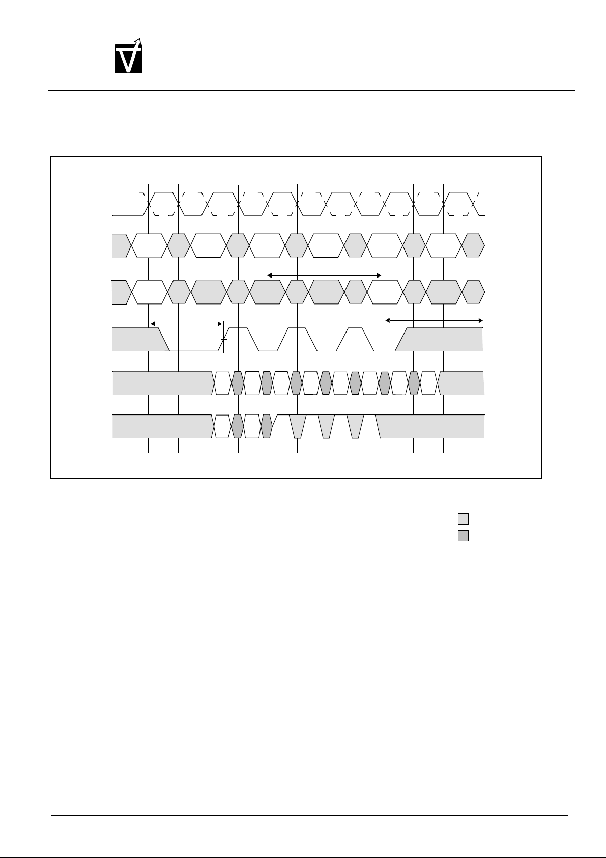
VIS
Preliminary VG37648041AT
256M:x4, x8, x16
CMOS Synchronous Dynamic RAM
CLK#
CLK
COMMAND
ADDRESS
DQS
DQ
DM
T0 T1
WRITE
Bank a,
Col b
T2 T3 T4 T5 T6 T7
t
DSS
max
NOP
Dl
b
NOP
T9
T8
NOP
t
WR
*2
*1
PRE
Bank,
(a or all)
*1
T10
NOP
t
RP
T11
Dl b =Data In for column b
An interrupted burst of 4 or 8 is shown, 2 data elements are written
1 subsequent element of Data In is applied in the programmed order following Dl b
tWR is referenced from the first positive CLK edge after the last desired Data In pair
A10 is LOW with the WRITE command (AUTO PRECHARGE is disabled)
*1=can be don’t care for programmed burst length of 4
*2=for programmed burst length of 4, DQS becomes don’t care at this point
Figure 30
WRITE TO PRECHARGE - MAX DSS, INTERRUPTING
DON’T CARE
UNDEFINED
Document : 1G5-0157 Rev.1 Page 56
Page 57
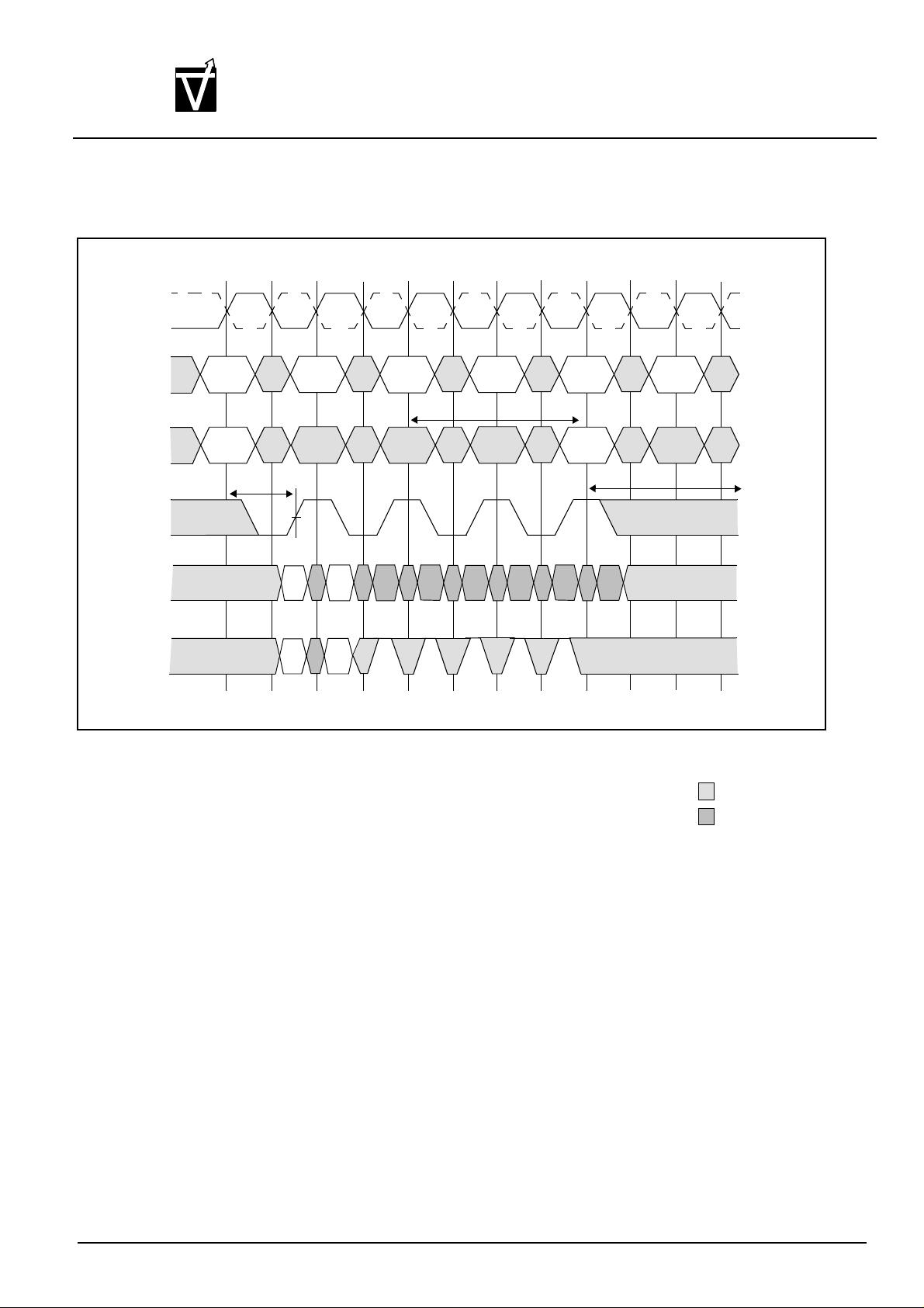
VIS
Preliminary VG37648041AT
256M:x4, x8, x16
CMOS Synchronous Dynamic RAM
CLK#
CLK
COMMAND
ADDRESS
DQS
DQ
DM
T0 T1
WRITE
Bank a,
Col b
t
DSS
min
T2 T3 T4 T5 T6 T7
NOP
Dl
b
NOP
t
WR
*2
*1
NOP
T9
T8
PRE
Bank,
(a or all)
*1
*1
T10
NOP
T11
t
RP
Dl b=Data In for column b
An interrupted burst of 4 or 8 is shown, 2 data elements are written
1 subsequent element of Data In is applied in the programmed order following Dl b
tWR is referenced from the first positive CLK edge after the last desired Data In pair
A10 is LOW with the WRITE command (AUTO PRECHARGE is disabled)
*1=can be don’t care for programmed burst length of 4
*2=for programmed burst length of 4, DQS becomes don’t care at this point
Figure 31
WRITE TO PRECHARGE - MIN DSS, INTERRUPTING
DON’T CARE
UNDEFINED
Document : 1G5-0157 Rev.1 Page 57
Page 58
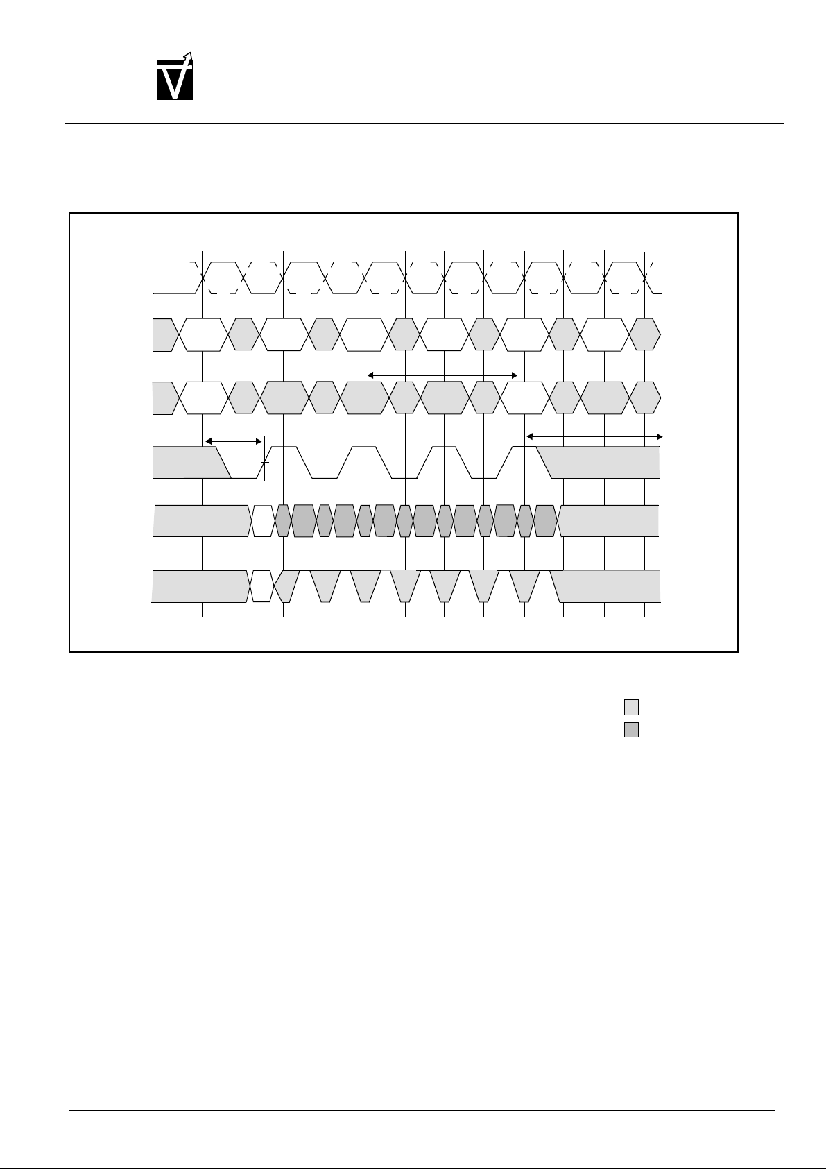
VIS
Preliminary VG37648041AT
256M:x4, x8, x16
CMOS Synchronous Dynamic RAM
CLK#
CLK
COMMAND
ADDRESS
DQS
DQ
DM
T0 T1
WRITE
Bank a,
Col b
t
DSS
min
T2 T3 T4 T5 T6 T7
NOP
Dl
b
NOP
t
WR
*2
NOP
T9
T8
PRE
Bank,
(a or all)
*1
*1
*1
T10
NOP
T11
t
RP
Dl b=Data In for column b
An interrupted burst of 4 or 8 is shown, 1 data elements are written
tWR is referenced from the first positive CLK edge after the last desired Data In pair
A10 is LOW with the WRITE command (AUTO PRECHARGE is disabled)
*1=can be don’t care for programmed burst length of 4
*2=for programmed burst length of 4, DQS becomes don’t care at this point
Figure 32
WRITE TO PRECHARGE - MIN DSS, ODD NUMBER OF DATA, INTERRUPTING
DON’T CARE
UNDEFINED
Document : 1G5-0157 Rev.1 Page 58
Page 59
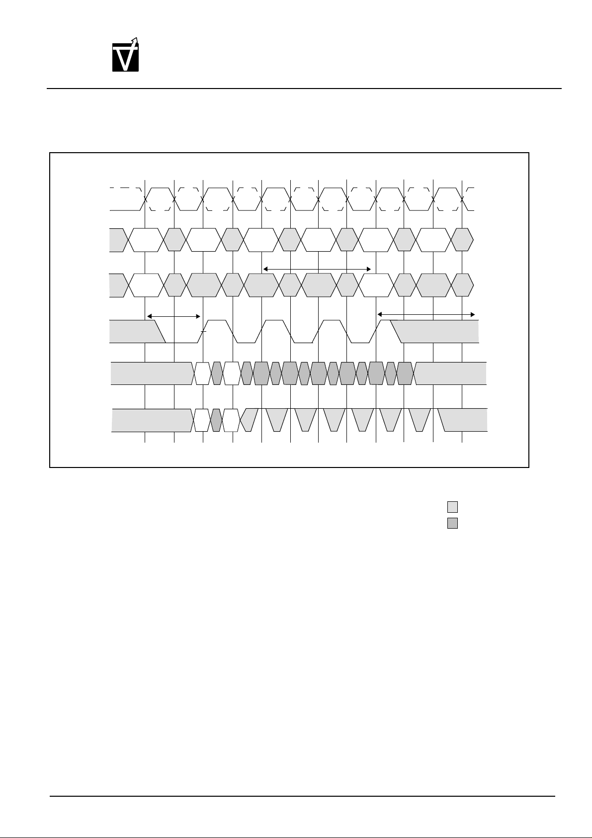
VIS
Preliminary VG37648041AT
256M:x4, x8, x16
CMOS Synchronous Dynamic RAM
CLK#
CLK
COMMAND
ADDRESS
DQS
DQ
DM
T0 T1
WRITE
Bank a,
Col b
t
DSS
nom
T2 T3 T4 T5 T6 T7
NOP
Dl
b
NOP
NOP
t
WR
*2
T8
PRE
Bank,
(a or all)
*1
T9
T10
NOP
t
RP
*1
T11
*1
Dl b=Data In for column b
An interrupted burst of 4 or 8 is shown, 2 data elements are written
1 subsequent element of Data In is applied in the programmed order following Dl b
tWR is referenced from the first positive CLK edge after the last desired Data In pair
A10 is LOW with the WRITE command (AUTO PRECHARGE is disabled)
*1=can be don’t care for programmed burst length of 4
*2=for programmed burst length of 4, DQS becomes don’t care at this point
Figure 33
WRITE TO PRECHARGE - NOMINAL DSS, INTERRUPTING
DON’T CARE
UNDEFINED
Document : 1G5-0157 Rev.1 Page 59
Page 60
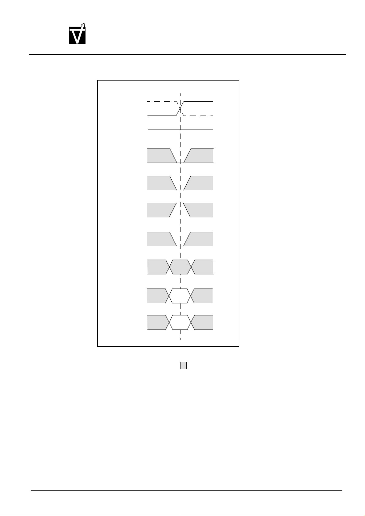
VIS
Preliminary VG37648041AT
256M:x4, x8, x16
CMOS Synchronous Dynamic RAM
CLK#
CLK
CKE
CS#
RAS#
CAS#
WE#
A0-A9,A11,A12
A10
HIGH
ALL BANKS
ONE BANK
BA0,1
BA=Bank Address (if A10 LOW, otherwise don’t care’)
Figure 34
PRECHARGE COMMAND
Document : 1G5-0157 Rev.1 Page 60
BA
=DON’T CARE
Page 61
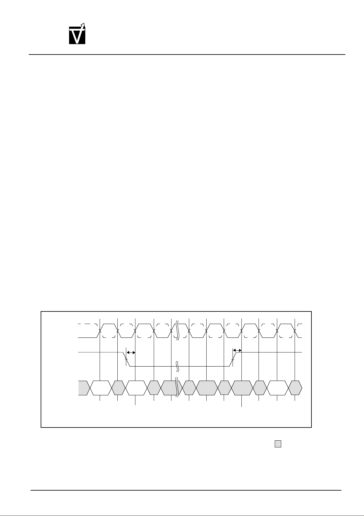
Preliminary VG37648041AT
VIS
CMOS Synchronous Dynamic RAM
PRECHARGE
The PRECHARGE command is used to deactivate the open row in a particular bank or the open
row in all banks. The bank(s) will be available for a subsequent row access some specified time (tRP)
after the PRECHARGE command is issued. Input A10 determines whether one or all banks are to be
precharged, and in the case where only one bank is to be prcharged, inputs BA0,BA1 select the bank.
When all banks are to be precharged, inputs BA0,BA1 are treated as “Don’t Care.” Once a bank has
been precharged, it is in the idle state and must be activated prior to any READ or WRITE commands
being issued to that bank.
POWER-DOWN
Power-down is entered when CKE is registered LOW (no accesses can be in progress). If power-
down occurs when all banks are idle, this mode is referred to as precharge power down; if powerdown occurs when there is a row active in either bank, this mode is referred to as active power-down.
Entering power-down deactivates the input and output buffers, excluding CLK, CLK# and CKE. For
maximum power savings, the user has the option of disabling the DLL prior to entering Power-down.
In that case, the DLL must be enabled after exiting power-down, and 200 clock cycles must occur
before a READ command can be issued. In either case, CKE LOW and a stable clock signal should
be maintained at the inputs of the DDR SDRAM, and all other input signals are “Don’t Care”. The
device may not remain in the power-down state loger than the refresh period (64ms) since no refersh
operations are performed in this mode.
The power-down state is exited when CKE is registered HIGH, and a command may be
256M:x4, x8, x16
applied be applied one clock cycle later.
CLK#
CLK
t
IS
CLK#
CLK
COMMAND
VALID
No column
access
in progress
NOP
Enter power-down
mode
Figure 35
POWER-DOWN
t
IS
Exit power-down
mode
VALID
DON’T CARE
Document : 1G5-0157 Rev.1 Page 61
Page 62
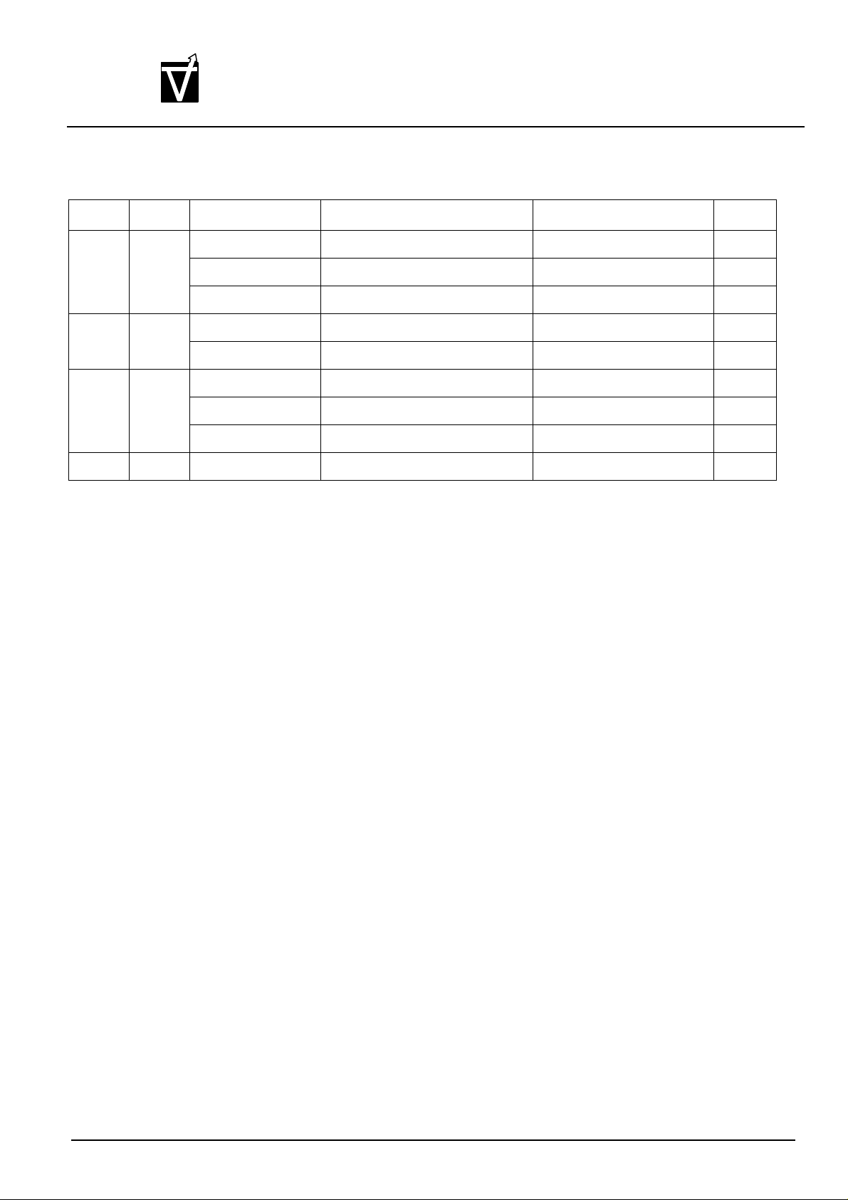
Preliminary VG37648041AT
VIS
256M:x4, x8, x16
CMOS Synchronous Dynamic RAM
TRUTH TABLE 2-CKE
(Notes: 1-4)
CKE
L L Power-Down X Maintain Power-Down
L H Power-Down COMMAND INHIBIT or NOP Exit Power-Down 5
H L All Banks Idle COMMAND INHIBIT or NOP Precharge Power-Down Entry
H H See Truth Table 3
n-1
CKE
CURRENT STATE COMAND
n
Self Refresh X Maintain Self Refresh
Self Refresh COMMAND INHIBIT or NOP Exit Self Refresh 6
Bank(s) Active COMMAND INHIBIT or NOP Active Power-Down Entry
All Banks Idle AUTO REFERESH Self Refresh Entry
n
ACTION
n
NOTES
NOTE: 1. CKEn is the logic state of CKE at clock edge n, CKE
2. Current state is the state of the DDR SDRAM immediately prior to clock edge n.
3. COMMANDn is the command registered at clock edge n, and ACTIONn is result of COMMAND
4. All states and sequences not shown are illegal or reserved.
5.Exiting power-down at clock edge n will put the device in the “all banks idle” state in time for clock edge n+1
6. Exiting self refreshh at clock edge n will put the device in the “all banks idle” state once tXSR is met. COMMAND INHIBIT or NOP commands should be issued on any clock edges occurring during the ‘XSR period. A
minimum of two NOP commands must be provided during t
needed before applying a read command, for the DLL to lock.
was the state of CKE at the previous clock edge.
n-1
period. A minimum of 200 clock cycles is
XSR
n-
Document : 1G5-0157 Rev.1 Page 62
Page 63
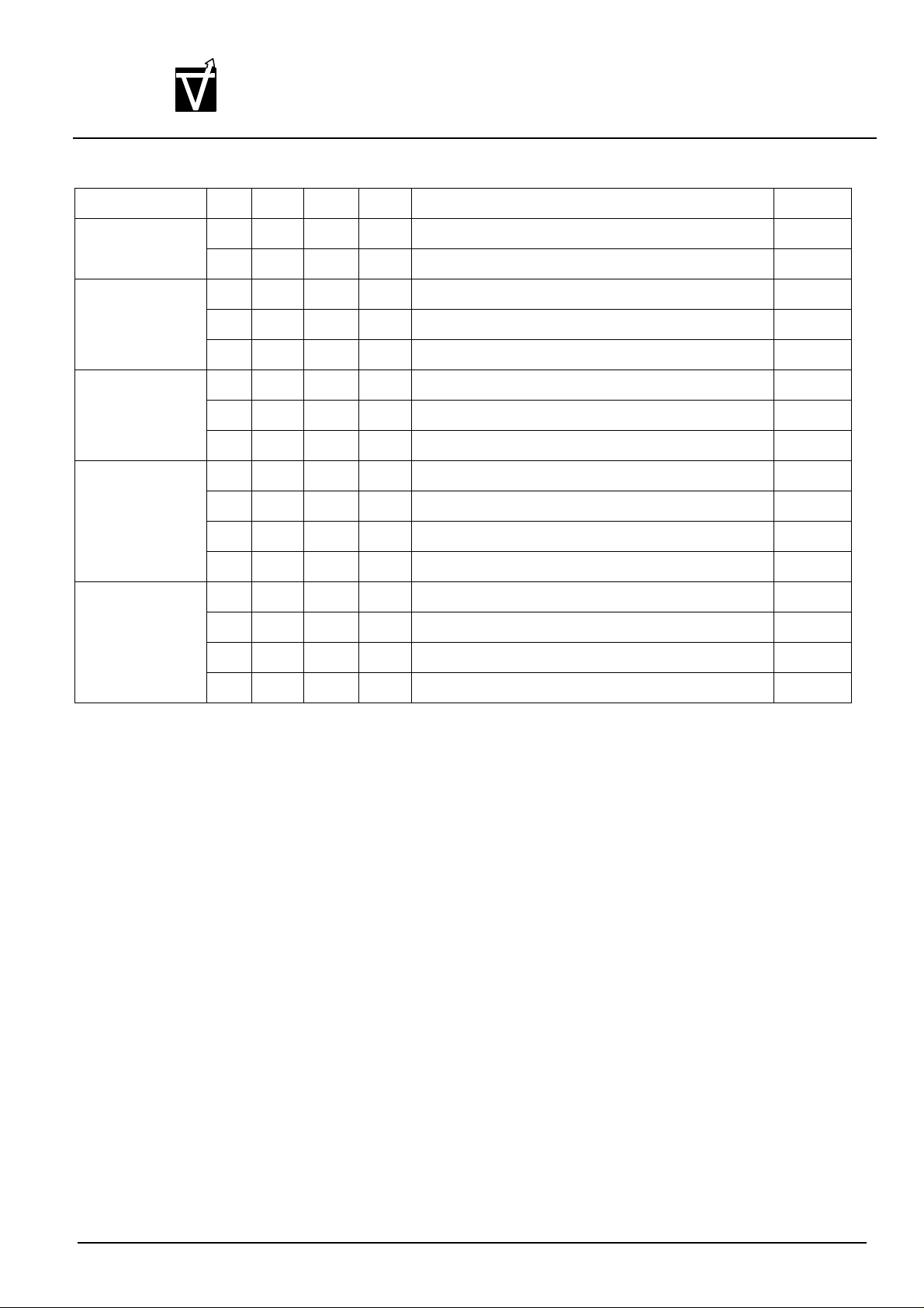
Preliminary VG37648041AT
VIS
256M:x4, x8, x16
CMOS Synchronous Dynamic RAM
TRUTH TABLE 3-Current State Bank n - Command to Bank n
(Notes: 1-6; notes appear below and on next page)
CURRENT STATE CS# RAS# CAS# WE# COMMANDACTION NOTES
Any H X X X COMMAND INHBIT (NOP/continue previous operation
L H H H NO OPERATION (NOP/continue previous operation)
L L H H ACTIVE (select and activate row)
Idle
Row Active
Read
(AutoPrecharge
Disabled)
Write
(AutoPrecharge
Disabled)
NOTE:
1. This table applies when CKE
been met (if the previous state was self refresh).
2. This table is bank-specific, except where noted, i.e., the current state is for a specific bank and the
commands shown are those allowed to be issued to that bank when in that state, Exceptions are
covered in the notes below.
3.Current state definitions:
L L L H AUTO REFRESH 7
L L L L LOAD MODE REGISTER 7
L H L H READ (select column and start READ burst) 10
L H L L WRITE (select column and start WRITE burst) 10
L L H L PRECHARGE (deactivate row in bank or banks) 8
L H L H READ (select column and start new READ burst) 10
L H L L WRITE (select column and start WRITE burst) 10
L L H L PRECHARGE(truncate READ burst, start PRECHARGE) 8
L H H L BURST TERMINATE 9
L H L H READ (select column and start READ burst) 10
L H L L WRITE (select column and start new WRITE burst) 10
L L H L PRECHARGE (truncate WRITE burst, start PRECHARGE) 8
was HIGH and CKEn Is HIGH (see Turn Table 2) and after tXSR has
n-1
Idle: The bank has been precharged, and tRP has been met.
Row Active: A row in the bank has been activated, and tRCD has been met. No data bursts/
accesses and no register accesses are in progress.
Read: A READ burst has been initiated, with AUTO PRECHARGE disabled, and has not yet termi-
nated or been terminated.
Write: A WRITE burst has been initiated, with AUTO PRECHARGE disabled, and has not yet ter-
minated or been terminated.
Document : 1G5-0157 Rev.1 Page 63
Page 64

Preliminary VG37648041AT
VIS
256M:x4, x8, x16
CMOS Synchronous Dynamic RAM
4. The following states must not be interrupted by a command issued to the same bank, COMMAND
INHIBIT or NOP commands, or allowable commands to the other bank should be issued on any clock
edge occurring during these states. Allowable commands to the other bank are determined by its current state and Truth Table3, and according to Truth Table 4.
Precharging: Starts with registration of a PRECHARGE command and ends when tRP is met. Once
t
RP is met, the bank will be in the idle state.
Row Activating: Starts with registration of an ACTIVE command and ends when tRCD is met. Once
t
RCD is met, the bank will be in the “row active” state.
Read w/AutoPrecharge Enabled: Starts with registration of a READ command with AUTO PRECHARGE
enabled and ends when tRP has been met. Once tRP is met, the bank will be
in the idle state.
Write w/Auto-
Precharge Enabled: Starts with registration of a WRITE command with AUTO PRECHARGE
enabled and ends when tRP has been met. Once tRP is met, the bank will be
in the idle state.
Write w/Auto
Precharge Enabled: Starts with registrayion of a WRITE command with AUTO PRECHARGE
enabled and ends when tRP has been met. Once tRP is met, the bank will be
in the idle state.
5.The following states must not be interrupted by any executable command; COMMAND INHIBIT or NOP
commands must be applied on each positive clock edge during these states.
Refreshing: Starts with registration of an AUTO REFERESH command and ends when tRC is met.
Once tRC is met, the DDR SDRAM will be in the “all banks idle” state.
Accessing Mode
Register: Starts with registration of a LOAD MODE REGISTER command and ends when tMTC has
been met. Once tMTC is met, the DDR SDRAM will be in the “all banks idle” state.
Precharging All: Starts with registration of a PRECHARGE ALL command and ends when tRP is
met. Once tRP is met, all banks will be in the idle state.
6. All states and sequences not shown are illegal or reserved.
7. Not bank-specific; reguired that all banks are idle.
8. May or may not be bank-specific; if all banks are to be precharged, all must be in a valid state for precharging.
9. Not bank-specific; BURST TERMINATE affects the most recent READ burst, regardless of bank.
10. READs or WRITEs listed in the Command/Action column include READs or WRITEs with AUTO
PRECHARGE enabled and READs or WRITEs with AUTO PRECHARGE disabled.
Document : 1G5-0157 Rev.1 Page 64
Page 65
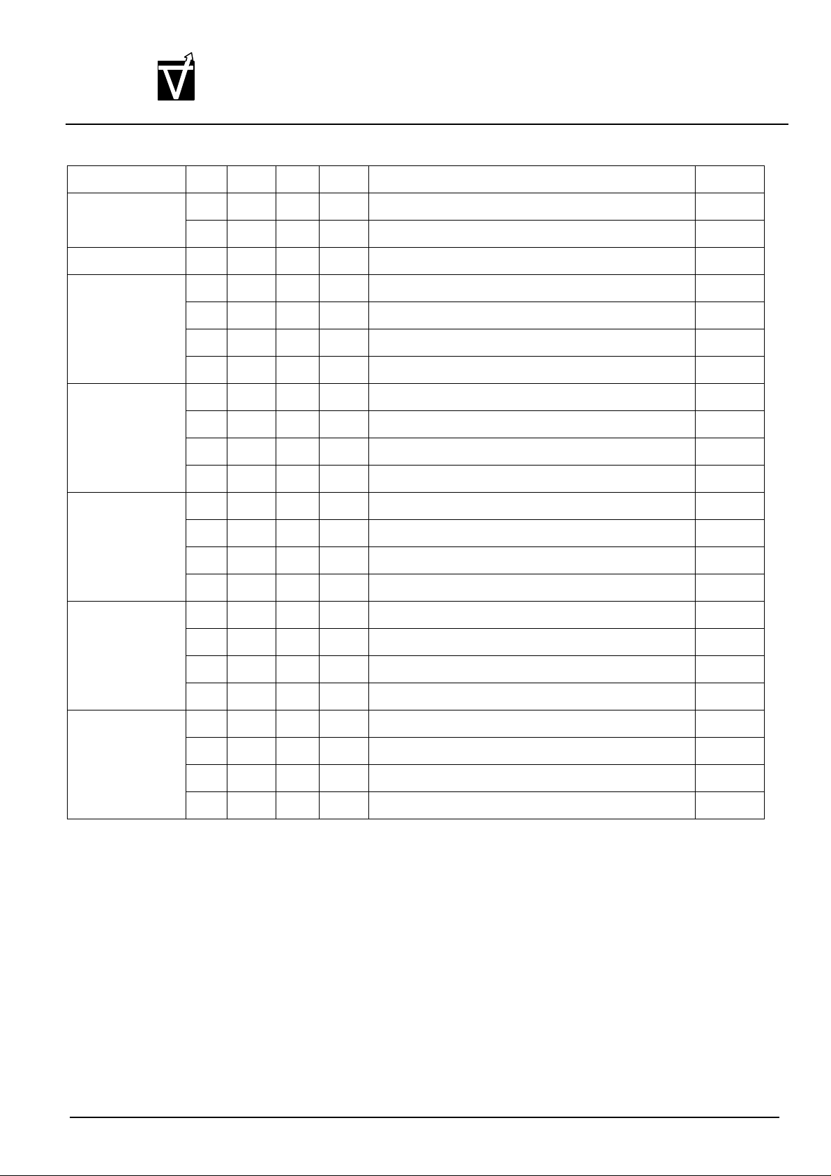
Preliminary VG37648041AT
VIS
256M:x4, x8, x16
CMOS Synchronous Dynamic RAM
TRUTH TABLE 4-Current State Bank n - Command to Bank m
(Notes: 1-6; notes appear below and on next page)
CURRENT STATE CS# RAS# CAS# WE# COMMANDACTION NOTES
Any H X X X COMMAND INHBIT (NOP/continue previous operation
L H H H NO OPERATION (NOP/continue previous operation)
Idle X X X X Any Command Otherwiswe Allowed to Bank m
Read
Activating,
Active, or
Precharging
Read
(AutoPrecharge
Disabled)
Write
(AutoPrecharge
Disabled)
Read
(With Auto-
Precharge)
L L H H ACTIVE (select andactivate row)
L H L H READ (select column and start READ burst) 7
L H L L WRITE(select column and start WRITE burst) 7
L L H L PRECHARGE
L L H H ACTIVE (select and activate row)
L H L H READ (select column and start new READ burst) 7
L H L L WRITE (select column and start WRITE burst) 7
L L H L PRECHARGE
L L H H ACTIVE (select and activate row)
L H L H READ (select column and start READ burst) 7
L H L L WRITE (select column and start new WRITE burst) 7
L L H L PRECHARGE
L L H H ACTIVE (select and activate row)
L H L H READ (select column and start new READ burst) 7
L H L L WRITE (select column and start WRITE burst) 7
L L H L PRECHARGE
Write
(With Auto-
Precharge)
NOTE:
1. This table applies when CKE
been met (if the previous state was self refresh).
2. This table describes alternate bank operation, except where noted, i.e., the current state is for bank n
and the commands shown are those allowed to be issued to bank m (assuming that bank m is in such
a state that the given command is allowable). Exceptions are covered in the notes below.
L L H H ACTIVE (select and activate row)
L H L H READ (select column and start READ burst) 7
L H L L WRITE (select column and start new WRITE burst) 7
L L H L PRECHARGE
was HIGH and CKEn Is HIGH (see Truth Table 2) and after tXSR has
n-1
Document : 1G5-0157 Rev.1 Page 65
Page 66

Preliminary VG37648041AT
VIS
CMOS Synchronous Dynamic RAM
3. Current state definitions:
Idle: The bank has been precharged, and tRP has been met.
Row Active: A row in the bank has been activated, and tRCD has been met. No data bursts/accesses
and no register accesses are in progress.
Read: A READ burst has been initiated, with AUTO PRECHARGE disabled, and has not yet termi-
nated or been terminated.
Write: A WRITE burst has been initiated, with AUTO PRECHARGE disabled, and has not yet termi-
nated or been terminated.
Read with Auto
Precharge Enabled: See following text
Write with Auto
Precharge Enabled: See following text
The Read with Auto Precharge Enabled or Write with Auto Precharge Enabled states can each be
broken into two parts: the access period and the precharge period. The precharge period is defined
as if the same burst was executed with Auto Precharge disabled and then followed with the earliest
possible PRECHARGE command that still accesses all of the data in the burst. The access period
256M:x4, x8, x16
starts with registration of the command and ends where the precharge period (or tRP) begins.
During the precharge period of the Read with Auto Precharge Enabled or Write with Auto Precharge
Enabled states, ACTIVE, PRECHARGE, READ and WRITE commands to the other bank may be
applied; during the access period, only ACTIVE and PRECHARGE commands to the other bank may
be applied. In either case, all other related limitations apply (e.g. following a Read with Auto Precharge by a Write command to another bank is subject to the same data path limitations as when following a Read by a Write).
4. AUTO REFERESH, LOAD MODE REGISTER and PRECHARGE ALL commands may only be issued
when all banks are idle.
5. A BURST TERMINATE command cannot be issued to another bank; it applies to the bank represented
by the current state only.
6. All states and sequences not shown are illegal or reserved.
7. READs or WRITEs listed in the Command/Action column include READs or WRITEs with AUTO PRECHARGE enabled and READs or WRITEs with AUTO PRECHARGE disabled.
Document : 1G5-0157 Rev.1 Page 66
Page 67
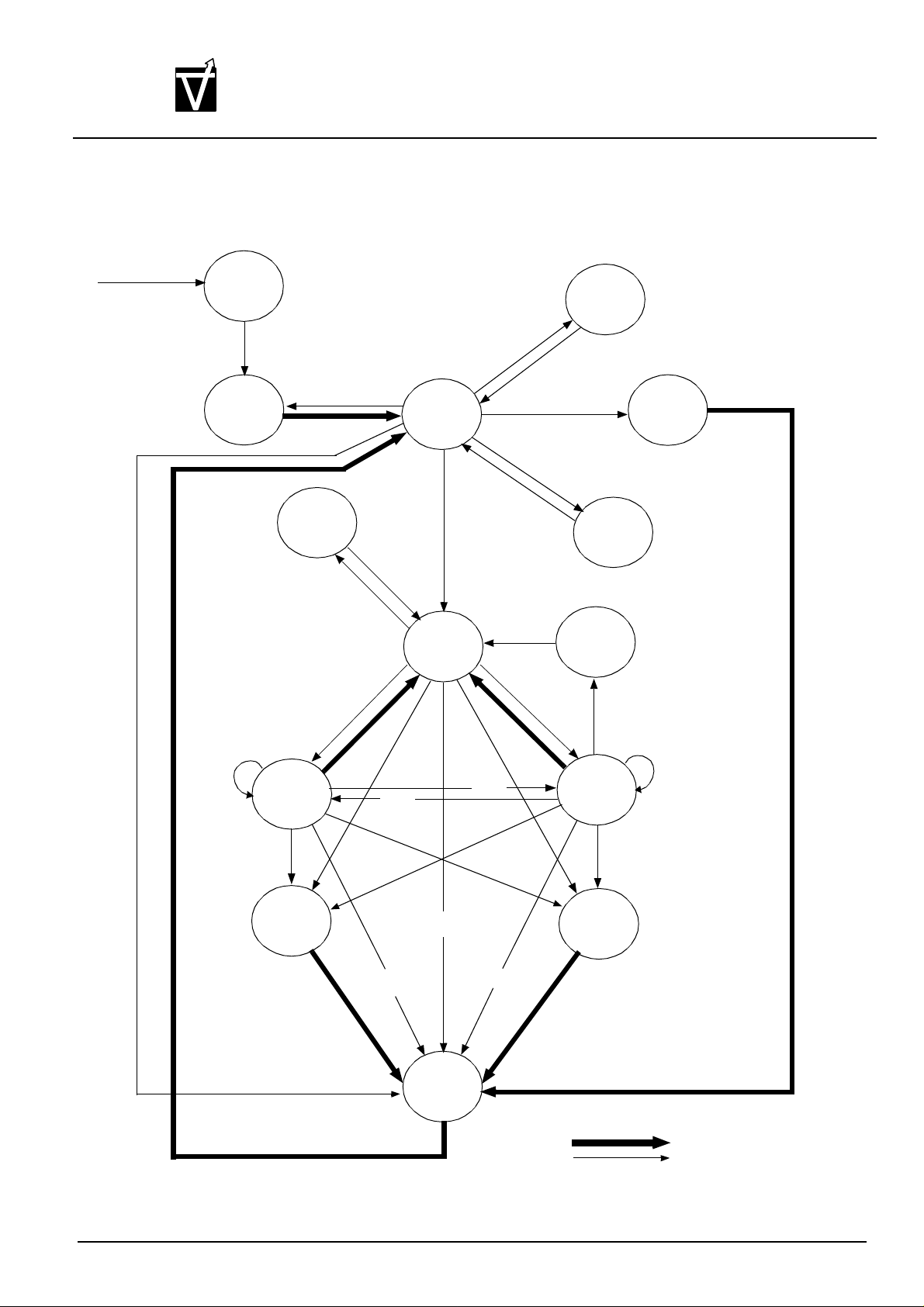
Preliminary VG37648041AT
VIS
CMOS Synchronous Dynamic RAM
Simplified state Diagram
Power
Applied
POWER
ON
MRS
EMRS
POWER
DOWN
MRS
IDLE
ACT
REFS
CKEH
REFSX
CKEL
REFA
256M:x4, x8, x16
SELF
REFRESH
AUTO
REFRESH
POWER
DOWN
WRITE
Write A
WRITE A
CKEL
Write
Write
A
Write
Write
PRE
CKEH
ROW
ACTIVE
Read
PRE
Read
Read
PRE
BURST STOP
Read
READ
Read A
A
READ A
PRE
Precharge
PREALL
Automatic Sequence
Command Sequence
Document : 1G5-0157 Rev.1 Page 67
Page 68
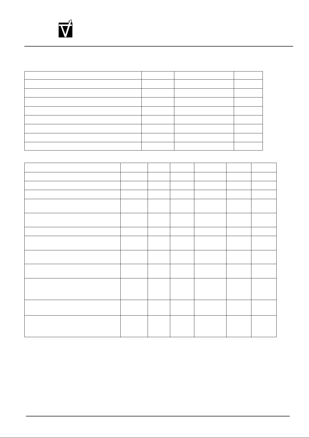
0VVINVDD
≤≥0VV
VDD
≤
≥
Preliminary VG37648041AT
VIS
CMOS Synchronous Dynamic RAM
Absolute Maximum ratings
Paramefer Sysbol Value Unit
Supply voltage relative to Vss (With VDD 3.3V) V
Voltage on VDDQ relative to Vss V
Voltage on input pin relative to Vss V
Voltage on I/O pin relative to Vss V
Short circuit output current V
Power dissipation P
Operating temperature (ambient) T
Storage temperature (plastic) PRE -55 to + 125 °C
Recommended DC Operating Conditions
Parameter Symbol Min
Supply voltage (with VDD 3.3V) V
I/O Supply Voltage V
I/O Reference Voltage V
I/O Termination Voltage (system) V
Input high Voltage, all inputs V
Input Low voltage, all inputs V
Input Voltage Level. CLK and CLK#
inputs
Input Differential Voltage, CLK and CLK#
inputs
Input Crossing Point Voltage, CLK and
CLK# inputs
Input Leakage Current
Any input
(All other pins not under test=0V)
Output Leakage Current
(DQs are disbled; )
Output Levels
Output High Current (V
Output Low current (V
out
=0.35V)
out
OUT
=1.95V)
Q
IH(DC)
IL(DC)
V
IN(DC)
V
ID(DC)
V
IX(DC)
I
I
I
DD
DDQ
REF
TT
I
I
OZ
OH
OL
DD
DDQ
IN
I/O
OUT
D
OPT
Typ
3.0 3.3
2.3 2.5 2.7 V
1.15 1.25 1.35 V 6
VREF-
0.04
VREF
+0.18
-0.3 - VREF-0.18 V
-0.3 - VDDQ+0.3 V
0.36 - VDD+0.6 V 8
1.15 - 1.35 V 9
-5 - 5 uA
-5 - 5 uA
-15.2 - -
VREF VREF+0.04 V 7
-1.0 + 4.6 V
-1.0 + 3.6 V
-1.0 + 3.6 V
-0.5 to VDDQ+0.5 V
50 mA
1.0 W
0 to + 70 °C
Max
3.6 V
- VDD+0.3 V
15.2
Unit Notes
mA
256M:x4, x8, x16
Document : 1G5-0157 Rev.1 Page 68
Page 69
VIS
0.2V
±
≥
≥
≥
≤
≤
CKE0.2V
≤
Capacitance
(Ta=25°C, f=1MHZ)
Preliminary VG37648041AT
256M:x4, x8, x16
CMOS Synchronous Dynamic RAM
Parameter Symbol Typ Max Unit NOTES
Input capacitance: CLK, CLK# C
Input capacitance (all input pins except data pins) C
Data input/output capacitance: DQs, DQS, DM C
Recommended Electrical Characteristic and D.C. Operating Conditions (VDDQ=+2.5,VDD=3.3V, Ta=0-70°C
Description/test condition Symbol
Operating Current: Active Mode
tRt
RCMIN()
CL=2.5, tCK=7ns for -8
Precharge Standby Current: Power-down mode, All banks idle
CKEVILMAX()
CL=2.5, tCK=7ns for -8
Precharge Standby Current: (MIN), All banks idle
CKEVILMIN()
CL=2.5, tCK=7ns for -8
, Burst=4, READ or Write
CSVIH≥
11
12
I/O
2.5 3.5 pF 13
2.5 3.5 pF 13
4.0 5.5 pF 13
Max Unit Notes
-75 -8
I
CC1
I
CC2P
I
CC2N
20
30
mA
Active Standby Current: (MIN), All banks active after t
met, no access in progress
CKEVILMIN()
CL=2.5, tCK=7ns for -8
Operating Current:
Burst=4, Continue burst
CKECILMAX()
transition once per clock cycle;
CL=2.5, tCK=7ns for-8
Auto refresh Current: I
Self Refresh Current:
CSVIH≥
READ or WRITE, All banks active, address
tRCt
RAS
≥
RCMIN()
I
I
I
CC3
CC4
CC5
CC6
180
210
2 11
Document : 1G5-0157 Rev.1 Page 69
Page 70
Preliminary VG37648041AT
VIS
CMOS Synchronous Dynamic RAM
AC OPERATIONS AND CONDITIONS:
Description Parameter Min. Max. Unit NOTES
Input High Voltage: DQ, DQS and DM signals VIH(AC) VREF+0.35 TBD V
256M:x4, x8, x16
Input Low Voltage: DQ, DQS and DM signals VIL(AC) TBD V
Input Differential Voltage, CLK and CLK# inputs VID(AC) 0.7 V
Input Crossing Point Voltage, CLK and CLK# inputs VIX(AC) 1.15 1.35 V 9
-0.35 V
REF
+0.6 V 8
DDQ
Document : 1G5-0157 Rev.1 Page 70
Page 71
VIS
0.2V±0.3V±0.2V
±
A.C Characteristics:
Preliminary VG37648041AT
256M:x4, x8, x16
CMOS Synchronous Dynamic RAM
Test Conditions: (Ta=0 to 70°C V
=2.5V , VDD=3.3V , or VDD=2.5V
DDQ
A.C. Parameter Symbol -75 -8 Unit Note
Access time from CLK/CLK# t
Clock high time t
Clock low time t
Clock cycle time CL=3 t
CL=2.5 t
CL=2 t
CL=1.5 t
Data-in hold time t
Data-in setup time t
Data-out high imedance from CLK/CLK# t
Data-out low impedance from CLK/CLK# t
DQS-DQ Skew t
DQ/DQS output valid time t
Write command to first DQS latching transition t
DQ/DQS input valid time t
LOAD MODE REGISTER COMMAND cycle time t
Write preamble setup time t
Write postamble t
Write command to DQS Low-Z t
Input hold time t
Input setup time t
Read preamble t
Read postamble t
ACTIVE to PRECHARGE command t
AUTO REFRESH, ACTIVE command period t
ACTIVE to READ or WRITE delay t
Refresh period (8192 rows) t
PRECHARGE command period t
ACTIVE bank A to Active bank B command t
Transition time t
Write recovery time t
Write data In to Read Command Delay t
Exit SELF REFRESH to ACTIVE command t
AC
CH
CL
CK3Q
CK2.5
CK2
CK15
DH
DS
HZ
LZ
DSDQ
DV
DSS
DSLH
MRD
WPR
WPO
WCP
IH
IS
RPR
RPO
RAS
RC
RCD
REF
RP
RRD
T
WR
WTR
XSR
Min. Max. Min. Max. t
-0.1 +0.1 -0.1 +0.1 t
0.45 0.55 0.45 0.55 t
CK
CK
CK
0.45 0.55 0.45 0.55 ns
5 15 6 15 ns
6.2 15 7 15 ns
7.5 15 8 15 ns
10 15 10 15 t
0.075 0.075 t
0.075 0.075 t
-0.1 +0.1 -0.1 +0.1 t
-0.1 +0.1 -0.1 +0.1 t
-0.075 +0.075 -0.075 +0.075 t
0.35 0.35 t
0.75 1.25 0.75 1.25 t
0.40 0.60 0.40 0.60 t
2 2 t
CK
CK
CK
CK
CK
CK
CK
CK
CK
CK
0 0 ns 19
0.4 0.6 0.4 0.6 t
CK
0 0 ns
0.15 0.15 t
0.15 0.15 t
0.9 1.1 0.9 1.1 t
0.4 0.6 0.4 0.6 t
CK
CK
CK
CK
45 120,000 48 120,000 ns
65 70 ns
20 20 ns
64 64 ms
20 20 ns
15 20 ns
ns
2 2 t
1 1 t
CK
CK
60 70 ns 21
18
18
22
20
Document : 1G5-0157 Rev.1 Page 71
Page 72
0.2V±3.3V
±
Preliminary VG37648041AT
VIS
CMOS Synchronous Dynamic RAM
NOTES
1. All voltages referenced to Vss.
2. Tests for AC timing, IDD, and electrical, AC and DC characteristics, may be conducted at nominal reference/supply voltage levels, but the related specifications and device operation are guaranteed for the full
voltage range specified.
3. Outputs measured with equivalent load:
V
TT
Ω
Ω
Output
25
(VOUT)
4.AC timing and IDD tests may use a VIL to VIH swing of up to 1.5V in the test environment, but input timing is
still referenced to V
teed for the specified AC input levels under normal use conditions. The minimum slew rate for the input sig-
nals used to test the device is 1V/ns in the range between V
5.The AC and DC input level specifications are as defined in the SSTL_2 Standard (i.e. the receiver will effectively switch as a result of the signal crossing the AC input level, and will remain in that state as long as the
signal does not ring back above (below) the DC input LOW(HIGH) level.
6.V
is expected to track variations in the DC level of V
REF
on V
7.VTT is not applied directly to the device. VTT is a system supply for signal termination resistors, is expected
to be set equal to V
8.VID is the magnitude of the difference between the input level on CLK and the input level on CLK#.
9.The value of VIX is expected to equal V
10.IDD is dependent on output loading and cycle rates.
Specified values are obtained with minimum cycle time and the outputs open.
11.Enables on chip refresh and address counters.
12.IDD specifications are tested after the device is properly initialized.
may not exceed +/-2% of the DC value.
REF
(or to the crossing point for CLK/CLK#), and parameter specifications are guaran-
REF
and must track variations in the DC level of V
REF
and must track variations in the DC level of V
REF
25
(Test point)
30pF
and V
IL(AC)
of the transmitting device. peak-to-peak noise
DDQ
REF
IH(AC)
.
.
.
REF
256M:x4, x8, x16
13.This parameter is sampled. VDDQ+2.5V , VDD=+3.3V , f=1MHz, tA=25°C
14.Input slew rate=1V/ns+/-20%.
15.The CLK/CLK# input reference level (for timeing referenced to CLK/CLK#) is the point at which CLK and
CLK# cross; the input reference level for signals other than CLK/CLK#, is VREF.
16.Inputs are not recognized as valid until V
lizes, CKE=<0.3V
17.The output timing reference level, as measured at the test point indicated in Note 3, is VTT.
18.tHZ and tLZ transitions occur in the same access time windows as valid data transitions. These parame-
ters are not referenced to a specific voltage level, but specify when the device output is no longer driving
(HZ), or begins driving (LZ).
19.The maximum limit for this parameter is not a device limit. The device will operate with a greater value for
this parameter, but system performance (bus turnaround) will degrade accordingly.
Document : 1G5-0157 Rev.1 Page 72
is recognized as LOW.
DDQ
stabilizes. Exceptions: during the period before V
REF
REF
stabi
Page 73

Preliminary VG37648041AT
VIS
CMOS Synchronous Dynamic RAM
20.The minimum limit for this parameter is not a device limit. The device will operate with a negative value for
this parameter, but system performance (bus turnaround) will degrade accordingly.
21.CLK must be toggled a minimum of two times during this period.
22.The specific reguirement is that DQS be valid (HIGH or LOW) on or befor this CLK edge. The case shown
(DQS going from High-Z to logic LOW) applies when no writes were previously in progress on the bus. If
a previous write was in progress. DQS could be HIGH at this time depending on tDSS.
256M:x4, x8, x16
Document : 1G5-0157 Rev.1 Page 73
Page 74
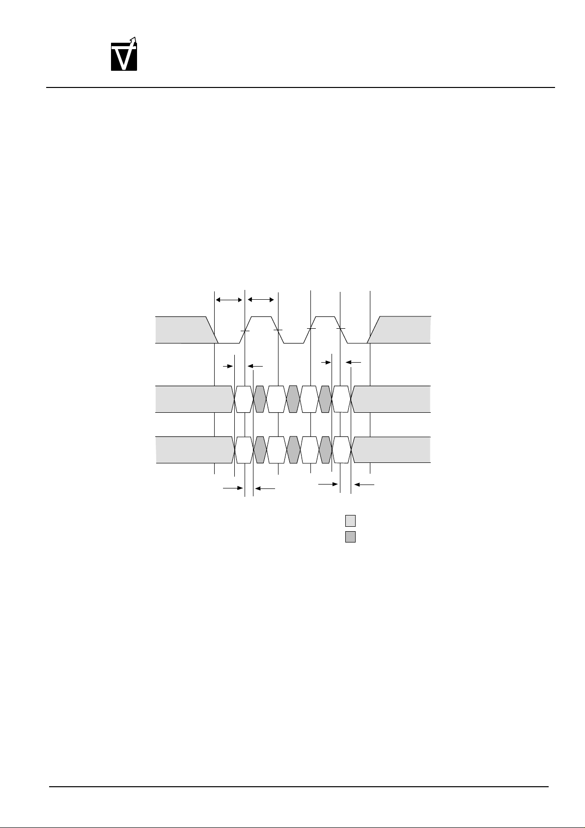
VIS
Preliminary VG37648041AT
256M:x4, x8, x16
CMOS Synchronous Dynamic RAM
DATA INPUT TIMING
DQS
DQ
DM
t
DSL
t
DS
Dl
n
t
DSH
t
DS
t
t
DH
DH
DON’T CARE
UNDEFINED
Dl n=Data In for column n
Burst Length=4 in the case shown
3 subsequent elements of Data In are applied in the programmed
order following Dl n
Document : 1G5-0157 Rev.1 Page 74
Page 75
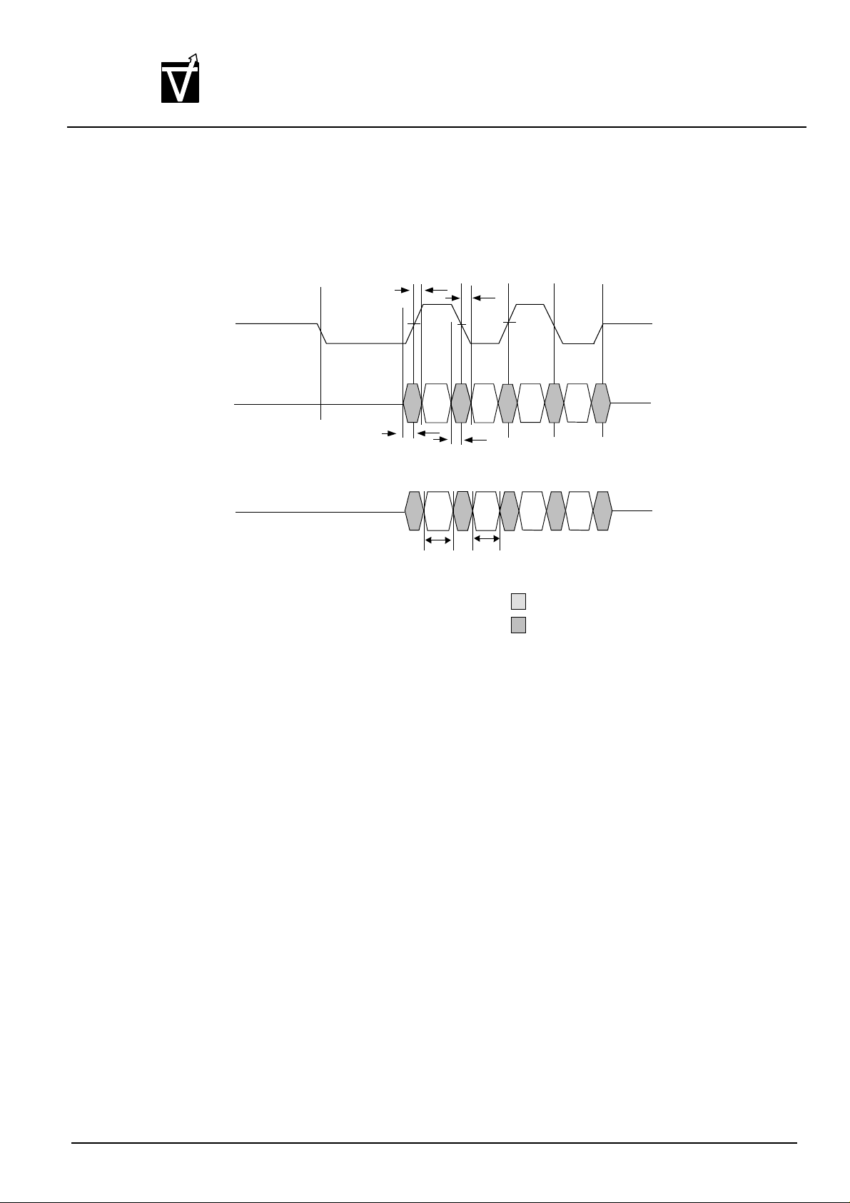
VIS
DQS
DQ
Preliminary VG37648041AT
256M:x4, x8, x16
CMOS Synchronous Dynamic RAM
DATA OUTPUT TIMING
t
t
DSDQ
min
DSDQ
min
Do
n
t
DSDQ
min
t
DSDQ
max
DQS,DO
Burst Length=4 in the case shown
t
DV
t
DV
DON’T CARE
UNDEFINED
Document : 1G5-0157 Rev.1 Page 75
Page 76
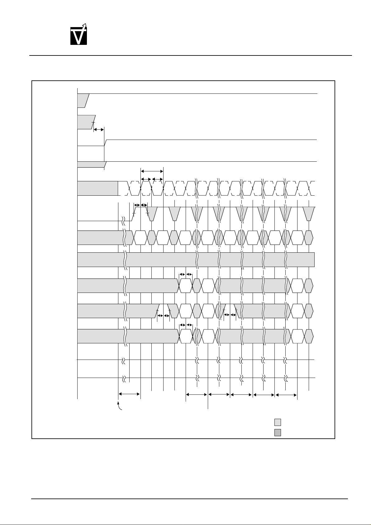
VIS
V
DD
V
DDQ
V
TT
(system*)
V
REF
CLK#
CLK
Preliminary VG37648041AT
256M:x4, x8, x16
CMOS Synchronous Dynamic RAM
INITIALIZE AND LOAD MODE REGISTERS
t
VTD
t
CK
t
t
CL
CH
t
IStIH
CKE
COMMAND
DM
A0,A9,
A11,A12
A10
BA0,BA1
DQS
DQ
LVCMOS LOW LEVEL
T=200
Power-up:
VDD and
CLK stable
NOP PRE
High-Z
High-Z
s
µ
ALL BANKS
t
IStIH
LMR
t
t
IS
CODE
CODE
t
t
IS
BA0=H,
BA1=L
Load
Extended
Mode
Register
IH
IH
t
MRD
LMR PRE
CODE
ALL BANKS
CODE
BA0=L,
BA1=L
200
cycles
of CLK...
Load
Base
Mode
Register
AR AR
t
t
IS
IH
t
RP
t
RC
ACT
RA
RA
BA
t
RC
DON’T CARE
UNDEFINED
•=VTT is not applied directly to the device, however t
must be greater than or equal to
VTD
zero to avoid device latch-up.
••=t
is required before any command can be applied, and 200 cycles of CLK are required before a
MRD
READ command can be applied.
Document : 1G5-0157 Rev.1 Page 76
Page 77
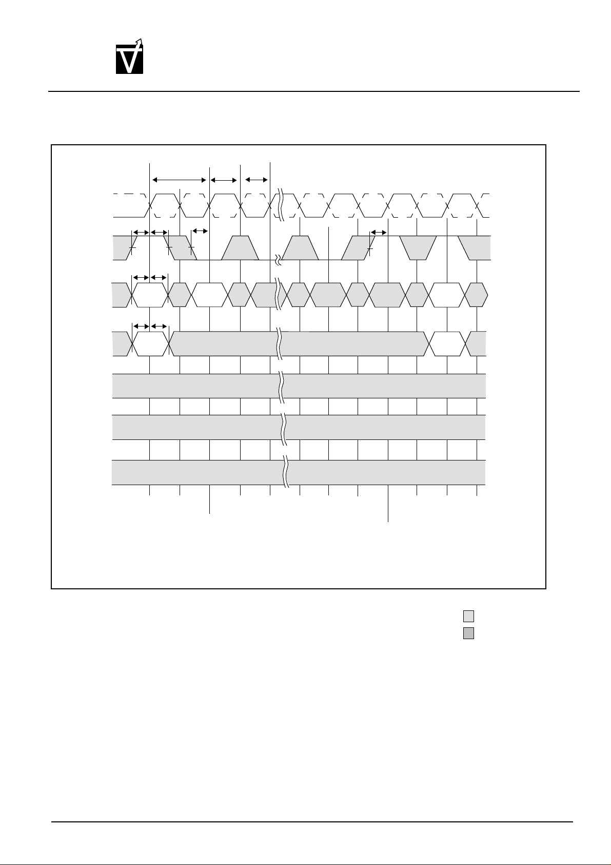
VIS
Preliminary VG37648041AT
256M:x4, x8, x16
CMOS Synchronous Dynamic RAM
POWER-DOWN MODE
CLK#
CLK
CKE
COMMAND
ADDR
DQS
DQ
t
IS
t
IS
VALID*
t
IS
VALID
t
CK
t
IH
t
IH
t
IH
t
t
IS
NOP
t
CH
CL
t
IS
VALID
VALID
DM
Enter
Power-Down
Mode
Exit
Power-Down
Mode
DON’T CARE
UNDEFINED
No column accesses are allowed to be in progress at the time Power-Down in entered
*= If this command is a PRECHARGE (or if the device is already in the idle state) then the Power-Down
mode shown is Precharge Power Down. If this command is an ACTIVE (or if at lease one row is already
active) then the Power-Down mode shown is Active Power Down.
Document : 1G5-0157 Rev.1 Page 77
Page 78
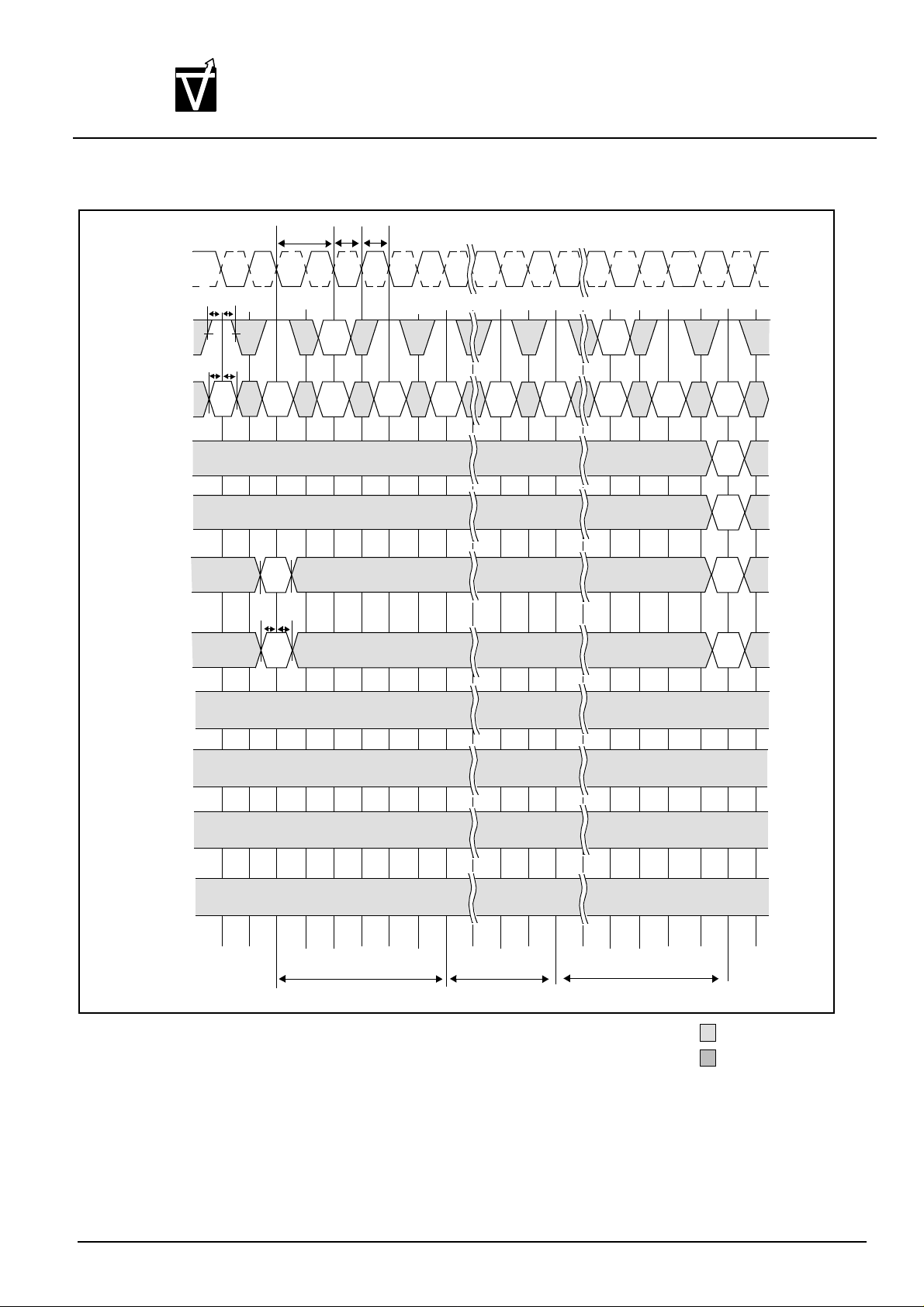
VIS
CLK#
CLK
Preliminary VG37648041AT
256M:x4, x8, x16
CMOS Synchronous Dynamic RAM
AUTO REFRESH MODE
t
CH
t
CL
t
CK
t
t
IS
IH
CKE
COMMAND
A0-A8
A9,A11,A12
A10
BA0,BA1
DQS
DQ
tISt
NOP
IH
PRE
ALL BANKS
ONE BANK
t
t
IS
IH
*Bank(s)
VALID
NOP
NOP
AR
NOP
AR
VALID
NOP
NOP ACT
RA
RA
RA
BA
DM
t
RP
t
RC
t
RC
DON’T CARE
UNDEFINED
DIS AP=Disable Autoprecharge
*=*Don’t Care”, if A10 is HIGH at this point; A10 must be HIGH if more than one bank is active(i.e. must pre-
charge all active banks)
PRE=PRECHARGE, ACT=ACTIVE, RA=Row Address, BA=Bank Address, AR=AUTOREFRESH
NOP commands are shown for ease of illustration; other valid commands may be possible at these times
DM, DQ and DQS signals are all *Don’t Care”/High-Z for operations shown
Document : 1G5-0157 Rev.1 Page 78
Page 79
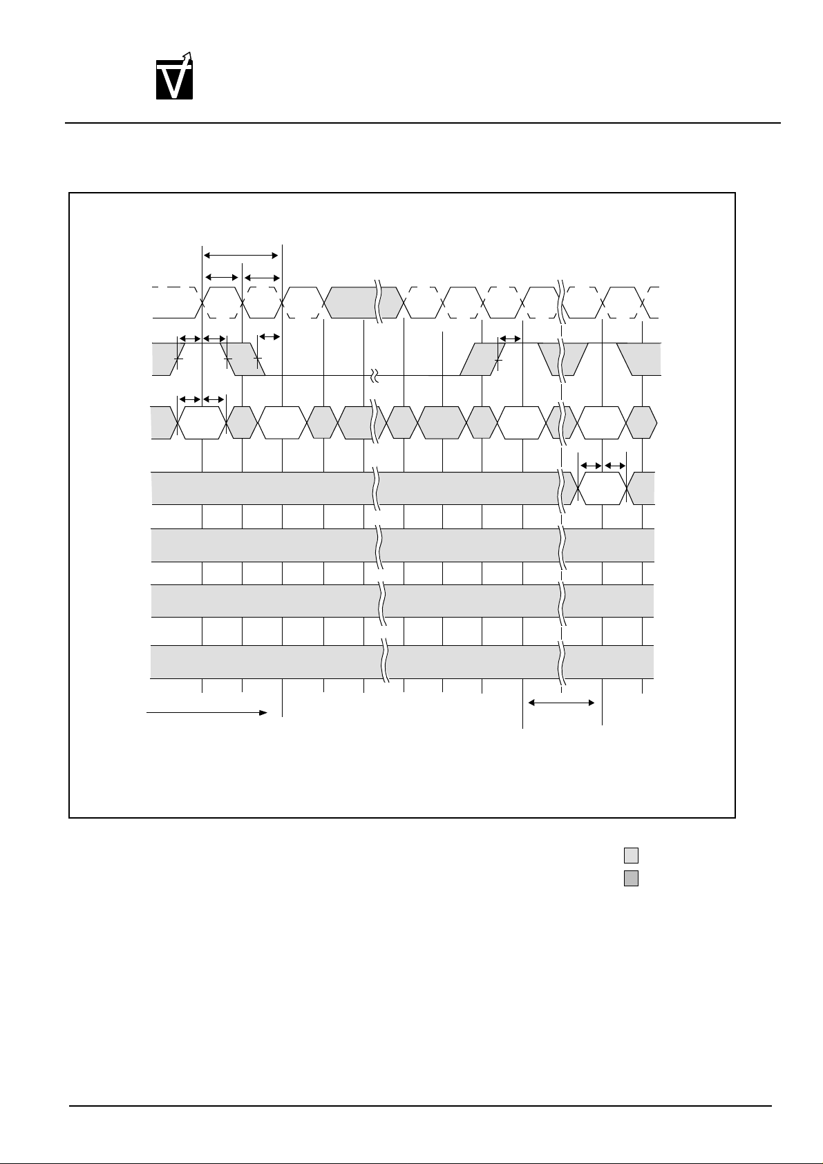
VIS
CLK#
CLK
CKE
Preliminary VG37648041AT
256M:x4, x8, x16
CMOS Synchronous Dynamic RAM
SELF REFRESH MODE
t
CK
t
t
CH
t
t
IH
IS
t
t
IS
IH
CL
t
IS
clock must be stable before
exiting Self Refresh mode
t
IS
COMMAND
ADDR
DQS
DQ
DM
t
RP*
NOP
AR
Enter
Self Refresh
Mode
NOP
EXIT
Self Refresh
Mode
200 cycles
of CLK**
VALID
t
IS
VALID
t
IH
DON’T CARE
UNDEFINED
*=Device must be in the “All banks idle” state prior to entering Self Refresh mode
**=tRC is required before any command can be applied, and 200 cycles of CLK are required before a READ
command can be applied.
The minimum time in Self Refresh mode is t
RAS
MIN.
Document : 1G5-0157 Rev.1 Page 79
Page 80
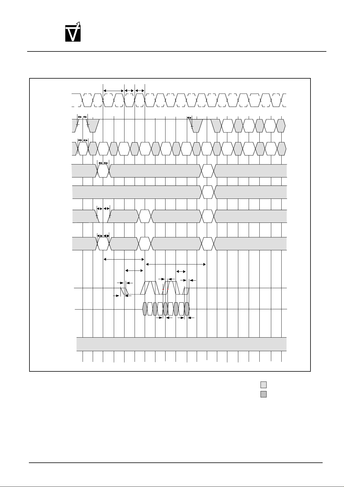
VIS
CLK#
CLK
Preliminary VG37648041AT
256M:x4, x8, x16
CMOS Synchronous Dynamic RAM
READ-WITHOUT AUTO PRECHARGE
t
CH
t
CL
t
IH
t
CK
t
t
IS
IH
CKE
COMMAND
x4:A0,A9,A11
x8:A0,A9
x16:A0,A8
x4:A12
x8:A9,A12
x16:A8,A9,A12
A10
BA0,BA1
DQS
tISt
NOP
VALID
IH
READ
tISt
Col n
t
t
IS
DIS AP
t
IS
Bank x
IH
IH
t
IH
NOP PRE
ALL BANKS
ONE BANK
*Bank x
CL=2
t
RPR
t
LZ
max
NOP
t
t
AC
max
RP
t
RPO
NOP
t
HZ
max
ACT
RA
RA
RA
Bank x
NOP
VALID
NOP NOP
VALID
t
LZ
DQ
min
DM
DO
n
t
min
AC
min
t
HZ
DON’T CARE
UNDEFINED
DO n=Data Out from column n
Burst Length=4 in the case shown
3 subsequent elements of Data Out are provided in the programmed order following Do n
DIS AP= Disable Autoprecharge
*=”Don’t Care”, if A10 is HIGH at this point
PRE=PRECHARGE, ACT=ACTIVE,RA=Row Address, BA=Bank Address
NOP commands are shown for ease of illustration; other commands may be valid at these times
Document : 1G5-0157 Rev.1 Page 80
Page 81
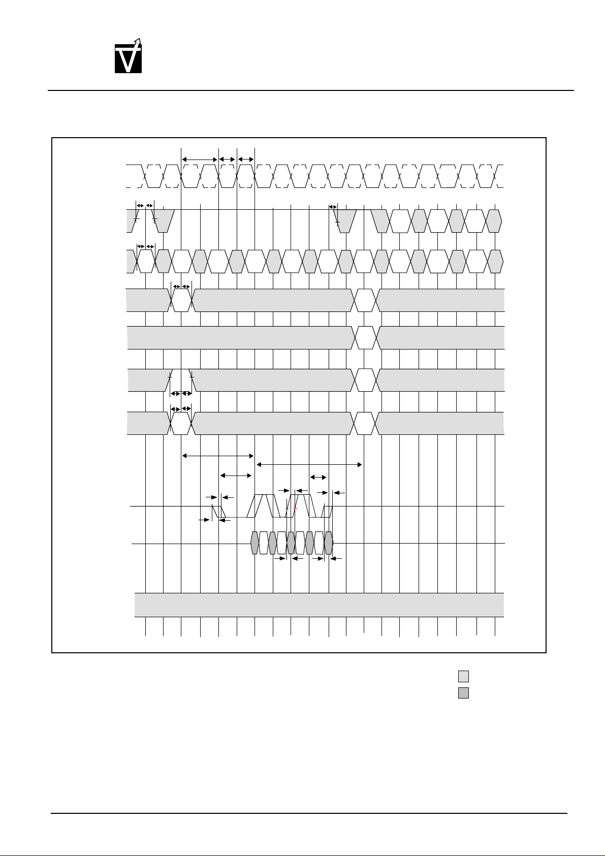
VIS
CLK#
CLK
Preliminary VG37648041AT
256M:x4, x8, x16
CMOS Synchronous Dynamic RAM
READ-WITH AUTO PRECHARGE
t
CH
t
CL
t
IH
t
CK
t
t
IS
IH
CKE
COMMAND
x4:A0,A9,A11
x8:A0,A9
x16:A0,A8
x4:A12
x8:A9,A12
x16:A8,A9,A12
A10
BA0,BA1
DQS
tISt
NOP
VALID
IH
READ
tISt
Col n
EN AP
t
IS
Bank x
IH
t
IH
NOP PRE
CL=2
t
RPR
t
LZ
max
NOP
t
t
AC
max
RP
t
RPO
NOP
t
HZ
max
ACT
RA
RA
RA
Bank x
NOP
VALID
NOP NOP
VALID
t
LZ
DQ
min
DM
DO
n
t
min
AC
min
t
HZ
DON’T CARE
UNDEFINED
DO n=Data Out from column n
Burst Length=4 in the case shown
3 subsequent elements of Data Out are provided in the programmed order following DO n
EN AP=Enable Autoprecharge
ACT=ACTIVE, RA=Row Address
NOP commands are shown for ease of illustration; other commands may be valid at these times
Document : 1G5-0157 Rev.1 Page 81
Page 82
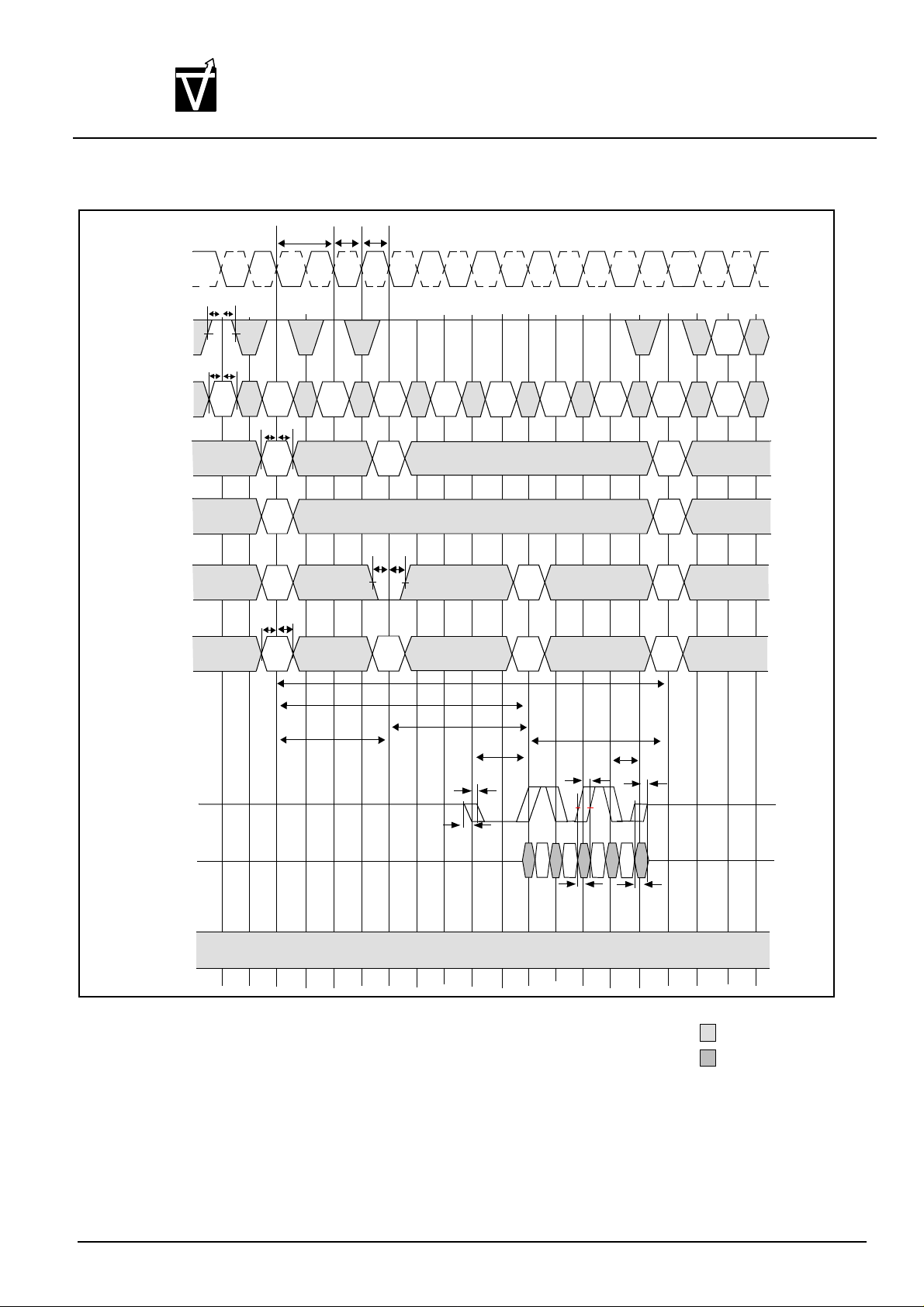
VIS
CLK#
CLK
Preliminary VG37648041AT
256M:x4, x8, x16
CMOS Synchronous Dynamic RAM
BANK READ ACCESS
t
CH
t
CL
t
CK
t
t
IS
IH
CKE
COMMAND
x4:A0,A9,A11
x8:A0,A9
x16:A0,A8
x4:A12
x8:A9,A12
x16:A8,A9,A12
A10
BA0,BA1
DQS
tISt
NOP
VALID
IH
t
RPO
ACT
Bank x
t
HZ
max
NOP
RA
RA
RA
ACT
tISt
RA
RA
RA
tISt
Bank x
IH
IH
NOP READ
t
t
RCD
Col n
t
IStIH
DIS AP
Bank x
RAS
NOP
CL=2
t
t
LZ
max
RPR
PRE
ALL BANKS
ONE BANK
*Bank x
NOP
NOP
t
RC
t
RP
t
AC
max
t
LZ
min
DQ
DM
DO
N
t
AC
min
t
min
HZ
DON’T CARE
UNDEFINED
DO n=Data Out from column n
Burst Length=4 in the case shown
3 subsequent elements of Data Out are provided in the programmed order following DO n
DIS AP=Disable Autoprecharge
*=”Don’t Care”, if A10 is HIGH at this point
PRE=PRECHARGE, ACT=ACTIVE, RA=Row Address, BA=Bank Address
NOP commands are shown for ease of illustration; other commands may be valid at these times
Document : 1G5-0157 Rev.1 Page 82
Page 83
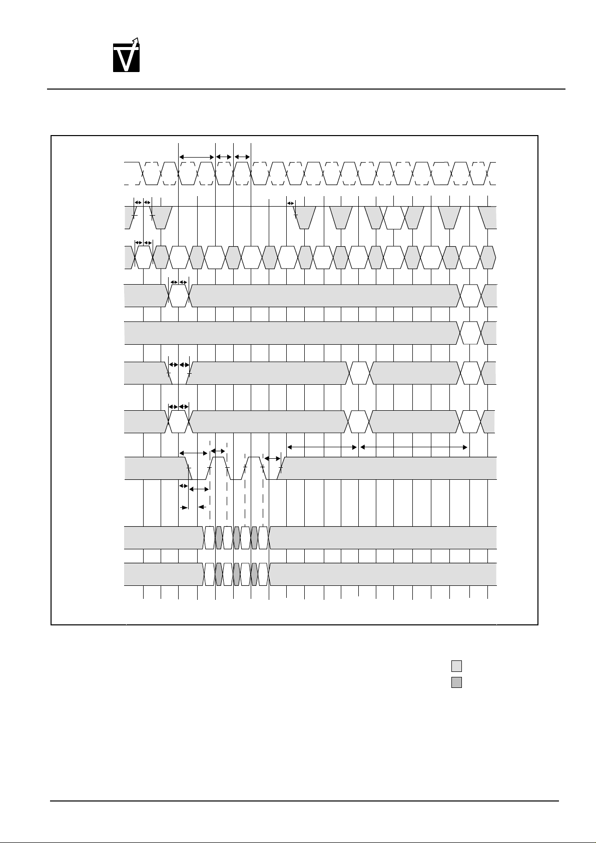
VIS
CLK#
CLK
Preliminary VG37648041AT
256M:x4, x8, x16
CMOS Synchronous Dynamic RAM
WRITE-WITHOUT AUTO PRECHARGE
t
CH
t
CL
t
IH
t
CK
t
t
IS
IH
CKE
COMMAND
x4:A0,A9,A11
x8:A0,A9
x16:A0,A8
x4:A12
x8:A9,A12
x16:A8,A9,A12
A10
BA0,BA1
DQS
DQ
tISt
NOP
VALID
IH
WRITE
tISt
Col n
t
IStIH
DIS AP
tISt
Bank x
t
WCP
IH
IH
t
WPR
t
DSS
t
NOP NOP
t
DSH
DSL
Dl
n
t
WPO
NOP
NOP
t
WR
PRE
ALL BANKS
ONE BANK
*Bank x
NOP
NOP
t
RP
ACT
RA
RA
RA
BA
DM
DON’T CARE
UNDEFINED
DI n=Data In for column n
Burst Length=4 in the case shown
3 subsequent elements of Data In are provided in the programmed order following DI n
DIS AP=Disable Autoprecharge
*=”Don’t Care”, if A10 is HIGH at this point
PRE=PRECHARGE, ACT=ACTIVE, RA=Row Address, BA=Bank Address
NOP commands are shown for ease of illustration; other commands may be possible at these times
Document : 1G5-0157 Rev.1 Page 83
Page 84
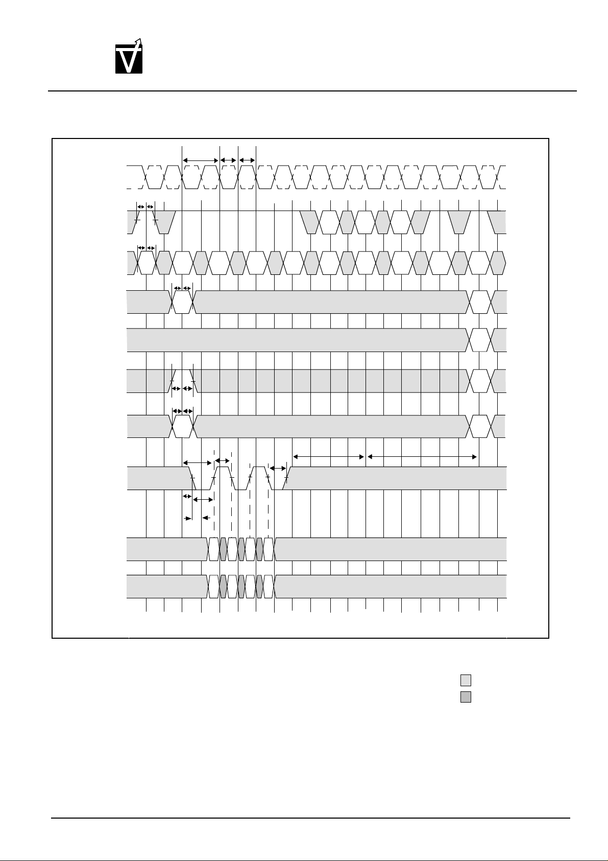
VIS
CLK#
CLK
Preliminary VG37648041AT
256M:x4, x8, x16
CMOS Synchronous Dynamic RAM
WRITE-WITH AUTO PRECHARGE
t
CH
t
CL
t
CK
t
t
IS
IH
CKE
COMMAND
x4:A0,A9,A11
x8:A0,A9
x16:A0,A8
x4:A12
x8:A9,A12
x16:A8,A9,A12
A10
BA0,BA1
DQS
tISt
NOP
VALID
IH
t
WPO
NOP
NOP
t
WR
EN AP
tISt
t
WCP
WRITE
tISt
Col n
Bank x
IH
IH
t
WPR
t
DSS
t
NOP NOP
t
DSH
DSL
VALID
NOP
VALID
NOP
NOP
t
RP
ACT
RA
RA
RA
BA
DQ
DM
Dl
n
DON’T CARE
UNDEFINED
DI n=Data In for column n
Burst Length=4 in the case shown
3 subsequent elements of Data In are provided in the programmed order following DI n
DIS AP=Disable Autoprecharge
*=”Don’t Care”, if A10 is HIGH at this point
PRE=PRECHARGE, ACT=ACTIVE, RA=Row Address, BA=Bank Address
NOP commands are shown for ease of illustration; other commands may be possible at these times
Document : 1G5-0157 Rev.1 Page 84
Page 85
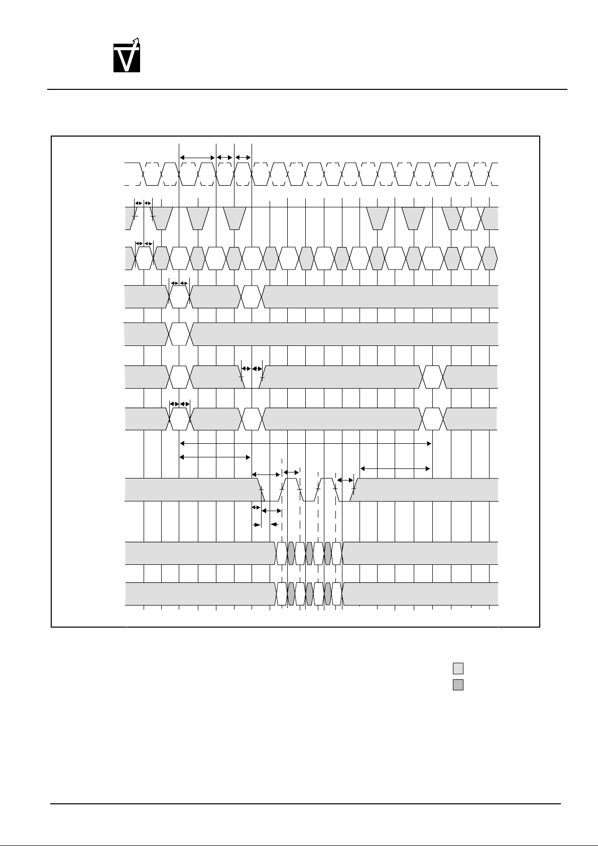
VIS
CLK#
CLK
Preliminary VG37648041AT
256M:x4, x8, x16
CMOS Synchronous Dynamic RAM
BANK WRITE ACCESS
t
CH
t
CL
t
CK
t
t
IS
IH
CKE
COMMAND
x4:A0,A9,A11
x8:A0,A9
x16:A0,A8
x4:A12
x8:A9,A12
x16:A8,A9,A12
A10
BA0,BA1
DQS
DQ
tISt
NOP
VALID
IH
ACT
tISt
RA
RA
RA
tISt
Bank x
IH
IH
NOP WRITE
t
RCD
t
Col n
t
IStIH
DIS AP
Bank x
WCP
t
t
RAS
t
DSS
WPR
t
DSL
Dl
n
NOP
t
DSH
NOP
t
WPO
NOP
NOP
t
WR
PRE
ALL BANKS
ONE BANK
*Bank x
NOP
DM
DON’T CARE
UNDEFINED
DI n=Data In for column n
Burst Length=4 in the case shown
3 subsequent elements of Data In are provided in the programmed order following DI n
DIS AP=Disable Autoprecharge
*=”Don’t Care”, if A10 is HIGH at this point
PRE=PRECHARGE, ACT=ACTIVE, RA=Row Address, BA=Bank Address
NOP commands are shown for ease of illustration; other commands may be possible at these times
Document : 1G5-0157 Rev.1 Page 85
Page 86
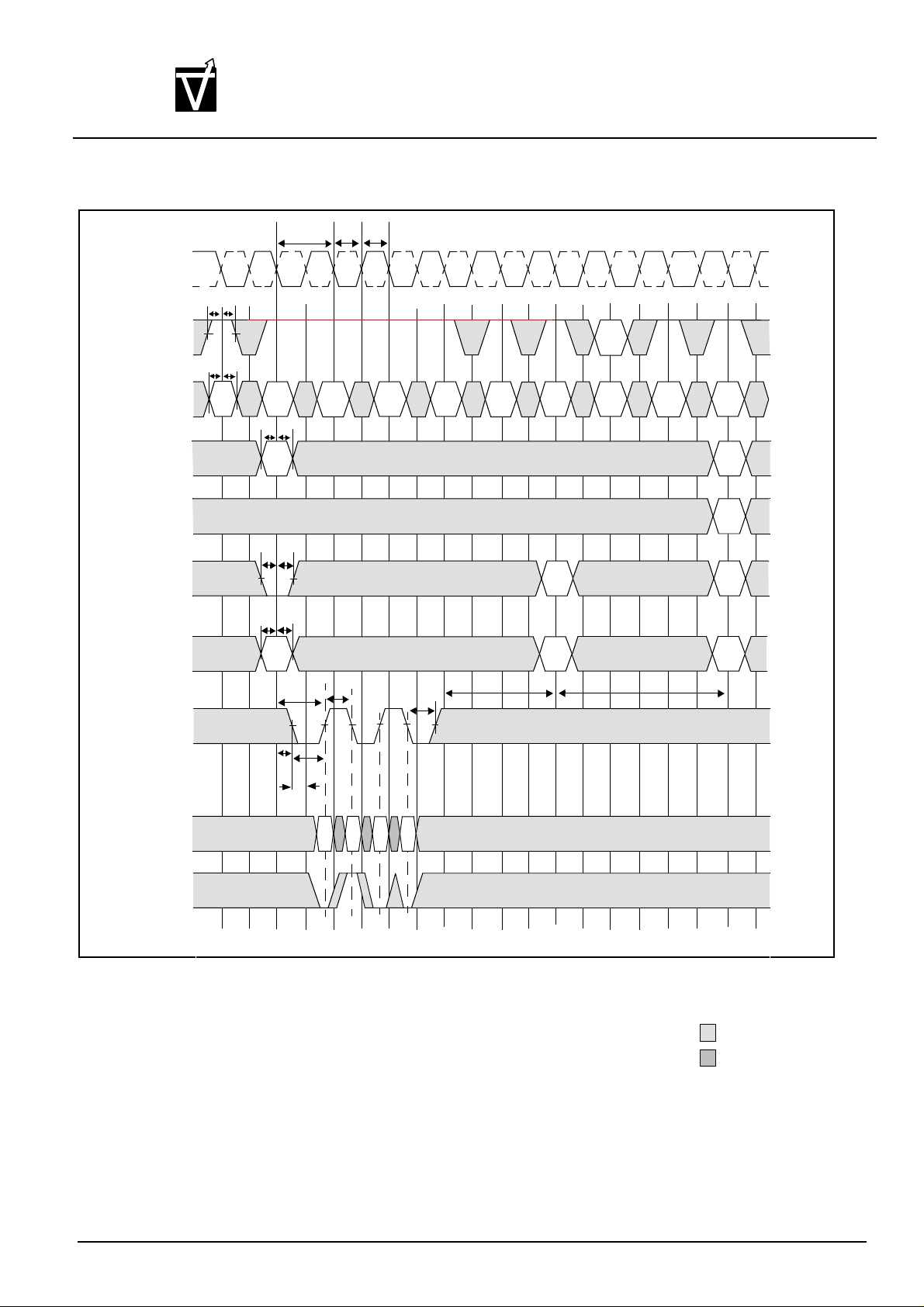
VIS
CLK#
CLK
Preliminary VG37648041AT
256M:x4, x8, x16
CMOS Synchronous Dynamic RAM
WRITE-DQM OPERATION
t
CH
t
CL
t
CK
t
t
IS
IH
CKE
COMMAND
x4:A0,A9,A11
x8:A0,A9
x16:A0,A8
x4:A12
x8:A9,A12
x16:A8,A9,A12
A10
BA0,BA1
DQS
DQ
tISt
NOP
VALID
IH
WRITE
tISt
Col n
t
IStIH
DIS AP
tISt
Bank x
t
WCP
IH
IH
t
WPR
t
DSS
t
NOP NOP
t
DSH
DSL
Dl
n
t
WPO
NOP
NOP
t
WR
PRE
ALL BANKS
ONE BANK
*Bank x
NOP
NOP
t
RP
ACT
RA
RA
RA
BA
DM
DON’T CARE
UNDEFINED
DI n=Data In for column n
Burst Length=4 in the case shown
3 subsequent elements of Data In are provided in the programmed order following DI n (The second element
of the four is masked)
DIS AP=Disable Autoprecharge
*=”Don’t Care”, if A10 is HIGH at this point
PRE=PRECHARGE, ACT=ACTIVE, RA=Row Address, BA=Bank Address
NOP commands are shown for ease of illustration; other commands may be possible at these times
Document : 1G5-0157 Rev.1 Page 86
 Loading...