

Page 1

0.3V
±
Preliminary VG3664321(4)1(2)BT
VIS
Description
The device is CMOS Synchronous Dynamic RAM organized as 524,288 - word x 32 - bit x 4 bank, and 1,048,576 - word x 32 - bit x 2 - bank, respectively. lt is fabricated with an advanced
submicron CMOS technology and designed to operate from a singly 3.3V only power supply. It is
packaged in JEDEC standard pinout and standard plastic TSOP package.
Features
• Single 3.3V () power supply
• High speed clock cycle time : 8/10 for LVTTL
• High speed clock cycle time : 8/10 for SSTL - 3
• Fully synchronous with all signals referenced to a positive clock edge
• Programmable CAS Iatency (2,3)
• Programmable burst length (1,2,4,8,& Full page)
• Programmable wrap sequence (Sequential/Interleave)
• Automatic precharge and controlled precharge
• Auto refresh and self refresh modes
• Dual Internal banks controlled by A11 (Bank select) for VG36643211(2)
• Quad Internal banks controlled by A11 & A12 (Bank select) for VG36643241(2)
• Each Banks can operate simultaneously and independently
• LVTTL compatible I/O interface for VG36643211 and VG36643241
• SSTL - 3 compatible I/O interface for VG36643212 and VG36643242
• Random column access in every cycle
• x32 organization
• Input/Output controlled by DQM0 ~ 3
• 4,096 refresh cycles/64ms
• Burst termination by burst stop and precharge command
• Burst read/single write option
CMOS Synchronous Dynamic RAM
Document : 1G5-0099 Rev.1 Page 1
Page 2
VIS
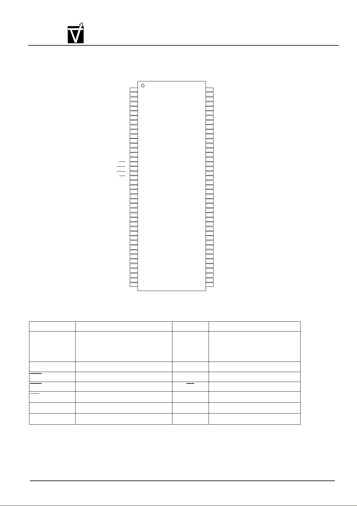
Pin Configuration
Preliminary VG3664321(4)1(2)BT
CMOS Synchronous Dynamic RAM
V
DD
DQ0
V
DDQ
DQ1
DQ2
V
SSQ
DQ3
DQ4
V
DDQ
DQ5
DQ6
V
SSQ
DQ7
NC
V
DD
DQM0
WE
CAS
RAS
CS
NC
A11/BA
NC
A10/AP
A0
A1
A2
DQM2
V
DD
NC
DQ16
V
SSQ
DQ17
DQ18
V
DDQ
DQ19
DQ20
V
SSQ
DQ21
DQ22
V
DDQ
DQ23
V
DD
1
2
3
4
5
6
7
8
9
10
11
12
13
14
15
16
17
18
19
20
21
22
23
24
25
26
27
28
29
30
31
32
33
34
35
36
37
38
39
40
41
42
43
86
85
84
83
82
81
80
79
78
77
76
75
74
73
72
71
70
69
68
67
66
65
64
63
62
61
60
59
58
57
56
55
54
53
52
51
50
49
48
47
46
45
44
V
SS
DQ15
V
SSQ
DQ14
DQ13
V
DDQ
DQ12
DQ11
V
SSQ
DQ10
DQ9
V
DDQ
DQ8
NC
V
SS
DQM1
NC (VREF)
NC
CLK
CKE
A9
A8
A7
A6
A5
A4
A3
DQM3
V
SS
NC
DQ31
V
DDQ
DQ30
DQ29
V
SSQ
DQ28
DQ27
V
DDQ
DQ26
DQ25
V
SSQ
DQ24
V
SS
Pin Description
VG36643211 (2)
Pin Name Function Pin Name Function
A0 - A11 Address inputs
DQM0 ~ 3 DQ Mask enable
- Row address A0 - A10
- Column address A0 - A8
A11 : Bank select
DQ0 ~ DQ31 Data - in/data - out CLK Clock input
RAS Row address strobe CKE Clock enable
CAS Column address strobe CS Chip select
WE Write enable V
V
SS
V
DD
Ground V
Power ( + 3.3V) (V
DDQ
SSQ
REF
Supply voltage for DQ
Ground for DQ
) Reference Voltage, SSTL - 3 only
Document : 1G5-0099 Rev.1 Page 2
Page 3
VIS
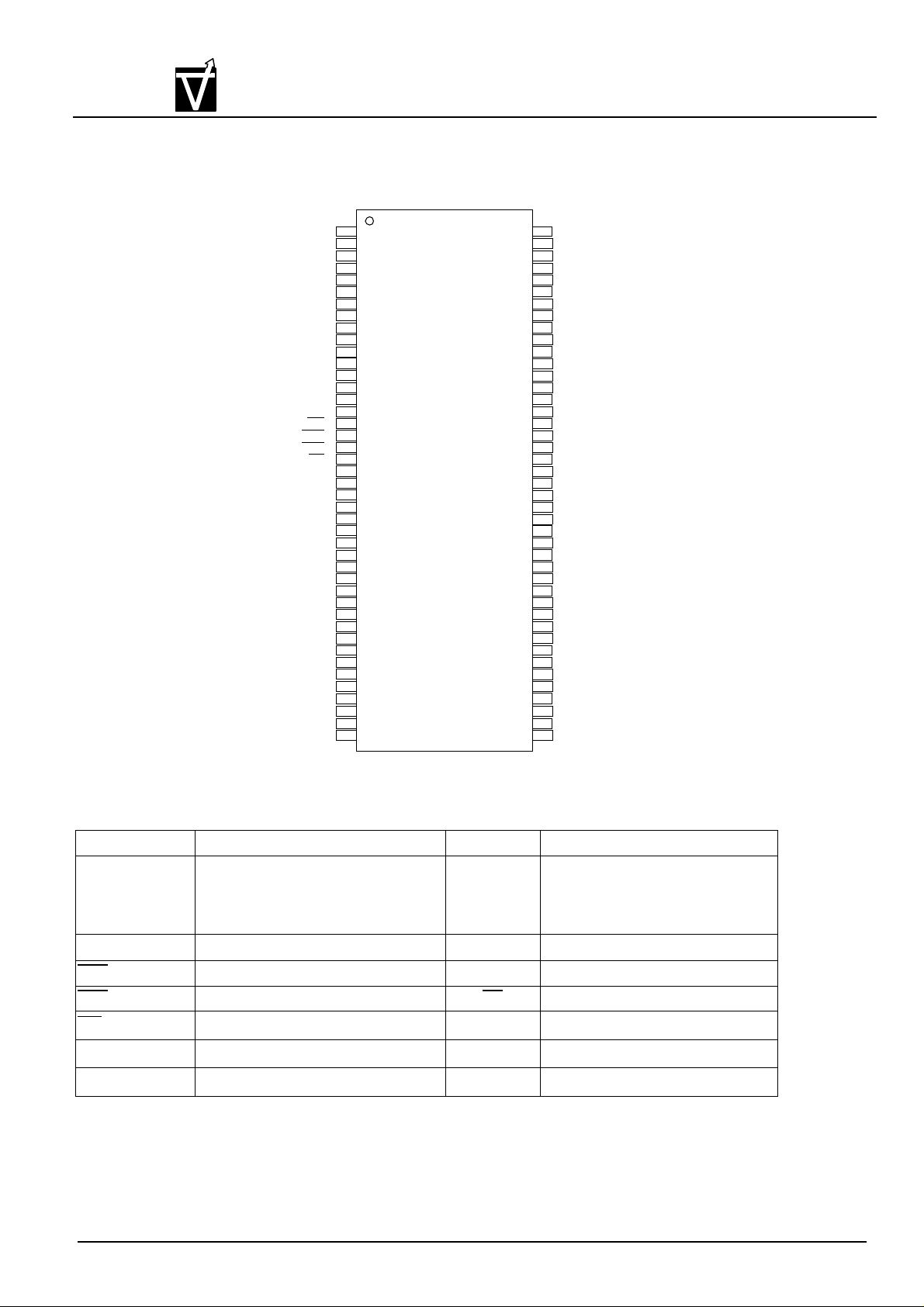
Pin Configuration
Preliminary VG3664321(4)1(2)BT
CMOS Synchronous Dynamic RAM
V
DD
DQ0
V
DDQ
DQ1
DQ2
V
SSQ
DQ3
DQ4
V
DDQ
DQ5
DQ6
V
SSQ
DQ7
NC
V
DD
DQM0
WE
CAS
RAS
CS
NC
A12/BA0
A11/BA1
A10/AP
A0
A1
A2
DQM2
V
DD
NC
DQ16
V
SSQ
DQ17
DQ18
V
DDQ
DQ19
DQ20
V
SSQ
DQ21
DQ22
V
DDQ
DQ23
V
DD
1
2
3
4
5
6
7
8
9
10
11
12
13
14
15
16
17
18
19
20
21
22
23
24
25
26
27
28
29
30
31
32
33
34
35
36
37
38
39
40
41
42
43
86
85
84
83
82
81
80
79
78
77
76
75
74
73
72
71
70
69
68
67
66
65
64
63
62
61
60
59
58
57
56
55
54
53
52
51
50
49
48
47
46
45
44
V
SS
DQ15
V
SSQ
DQ14
DQ13
V
DDQ
DQ12
DQ11
V
SSQ
DQ10
DQ9
V
DDQ
DQ8
NC
V
SS
DQM1
NC (VREF)
NC
CLK
CKE
A9
A8
A7
A6
A5
A4
A3
DQM3
V
SS
NC
DQ31
V
DDQ
DQ30
DQ29
V
SSQ
DQ28
DQ27
V
DDQ
DQ26
DQ25
V
SSQ
DQ24
V
SS
Pin Description
VG36643241 (2)
Pin Name Function Pin Name Function
A0 - A12 Address inputs
DQM0 ~ 3 DQ Mask enable
- Row address A0 - A10
- Column address A0 - A7
A11 & A12 : Bank select
DQ0 ~ DQ31 Data - in/data - out CLK Clock input
RAS Row address strobe CKE Clock enable
CAS Column address strobe CS Chip select
WE Write enable V
V
SS
V
DD
Ground V
Power ( + 3.3V) (V
DDQ
SSQ
REF
Supply voltage for DQ
Ground for DQ
) Reference Voltage, SSTL - 3 only
Document : 1G5-0099 Rev.1 Page 3
Page 4
VIS
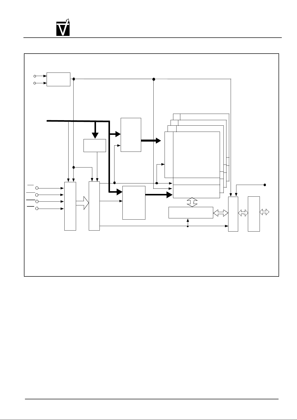
Block Diagram
Preliminary VG3664321(4)1(2)BT
CMOS Synchronous Dynamic RAM
CLK
CKE
Address
CS
RAS
CAS
WE
Clock
Generator
Row
Address
Buffer
Mode
Register
Control Logic
Command Decoder
&
Refresh
Counter
Column
Address
Buffer
&
Burst
Counter
Row Decoder
Column Decoder &
Latch Circuit
Data Control Circuit
(Bank D)
(Bank C)
Bank B
Bank A
Sense Amplifier
DQM
DQ
Buffer
Latch Circuit
Input & Output
Note: Bank C and Bank D are for VG36643241(2) only
Document : 1G5-0099 Rev.1 Page 4
Page 5
≤
Preliminary VG3664321(4)1(2)BT
VIS
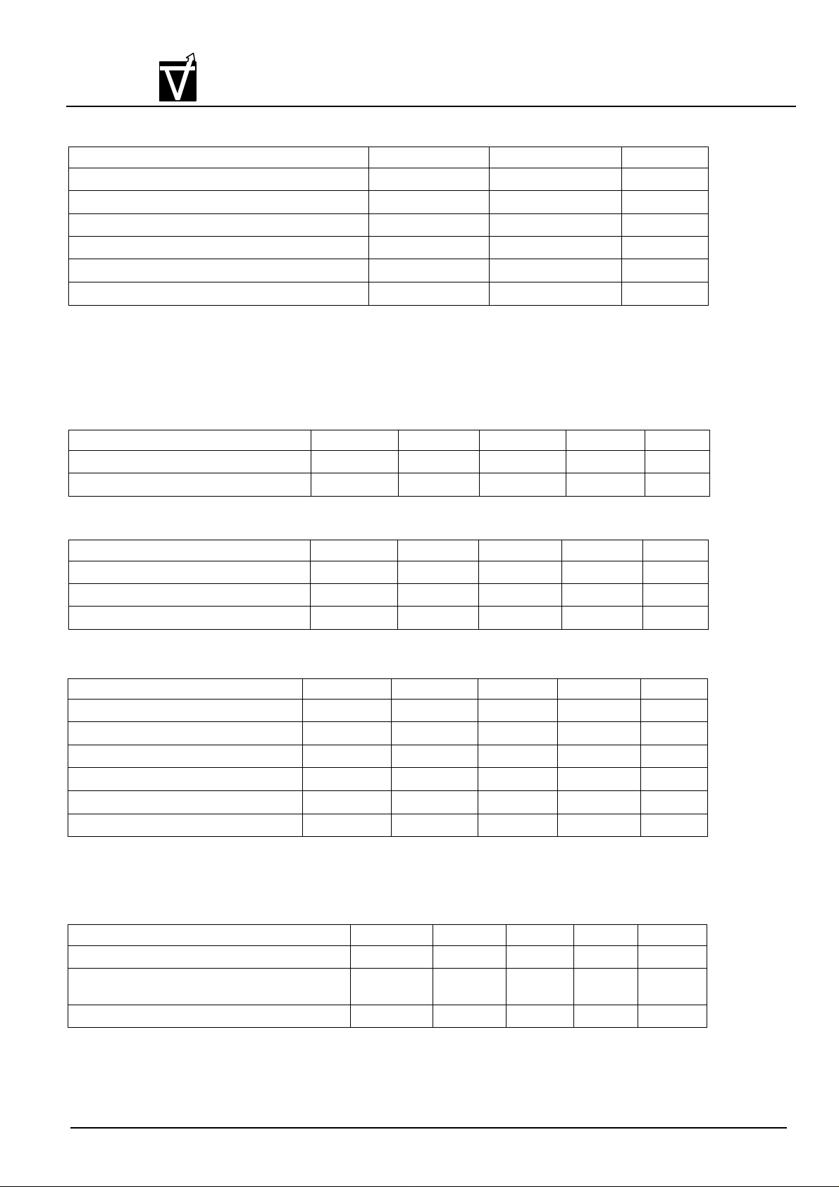
Absolute Maximum D.C. Ratings
Voltage on any pin relative to Vss VIN, V
Supply voltage relative to Vss VDD, V
Short circuit output current I
Power dissipation P
Operating temperature T
Storage temperature T
Caution Exposing the device to stress above those listed in Absolute Maximum Ratings could cause
permanent damage. The device is not meant to be operated under conditions outside the limits
described in the operational section of this specification. Exposure to Absolute Maximum Rating
conditions for extended periods may affect device reliability.
Maximum A.C. Operating Requirements for LVTTL Compatible
Parameter Symbol Min Max Unit Notes
Input High Voltage V
Input Low Voltage V
CMOS Synchronous Dynamic RAM
Parameter Symbol Value Unit
OUT
DDQ
OUT
D
OPT
STG
IH
IL
2.0 V
V
-2.0 0.8 V 2
SSQ
-0.5 to + 4.6 V
-0.5 to + 4.6 V
50 mA
1.0 W
0 to + 70 °C
-55 to + 125 °C
+ 2.0 V 2
DDQ
Recommended DC Operating Conditions for LVTTL Compatible
Parameter Symbol Min Typ Max Unit
Supply Voltage V
DD, VDDQ
Input High Voltage, all inputs V
Input Low Voltage, all inputs V
IH
IL
3.0 3.3 3.6 V
2.0 - V
-0.3 - 0.8 V
Recommended DC Operating Conditions for SSTL - 3 Interface
Parameter Symbol Min Typ Max Unit
Supply Voltage V
Supply Voltage (Ground) V
DD, VDDQ
SS, VSSQ
Reference Voltage V
Termination Voltage V
Input High Voltage, all inputs V
Input Low Voltage, all inputs V
REF
TT
IH(dc)
IH(dc)
3.0 3.3 3.6 V
0 - 0 V
1.3 1.5 1.7 V
V
-005 V
REF
V
+ 0.2 - V
REF
REF
-0.3 - V
Capacitance
(Ta = 25°C, f = 1MHZ)
Parameter Symbol Typ Max Unit Notes
Input capacitance (Address) C
Input capacitance (all input pins
I1
C
I2
- 4 pF 1
- 4 pF 1
except address pins & data pins.)
Data input/output capacitance C
Notes : 1. Capacitance measured with effective capacitance measuring method.
2. The overshoot and undershoot voltage duration is 3ns with no input clamp diodes.
I/O
- 5 pF 1
+ 0.3 V
DD
V
+ 0.05 V
REF
+ 0.3 V
DD
-0.2 V
REF
Document : 1G5-0099 Rev.1 Page 5
Page 6
≥≤≤
∞
≥≥≥
∞
≤≤≤
∞
≥≥≥
∞
≤≥≤
≥≤≥≤µ
Preliminary VG3664321(4)1(2)BT
VIS
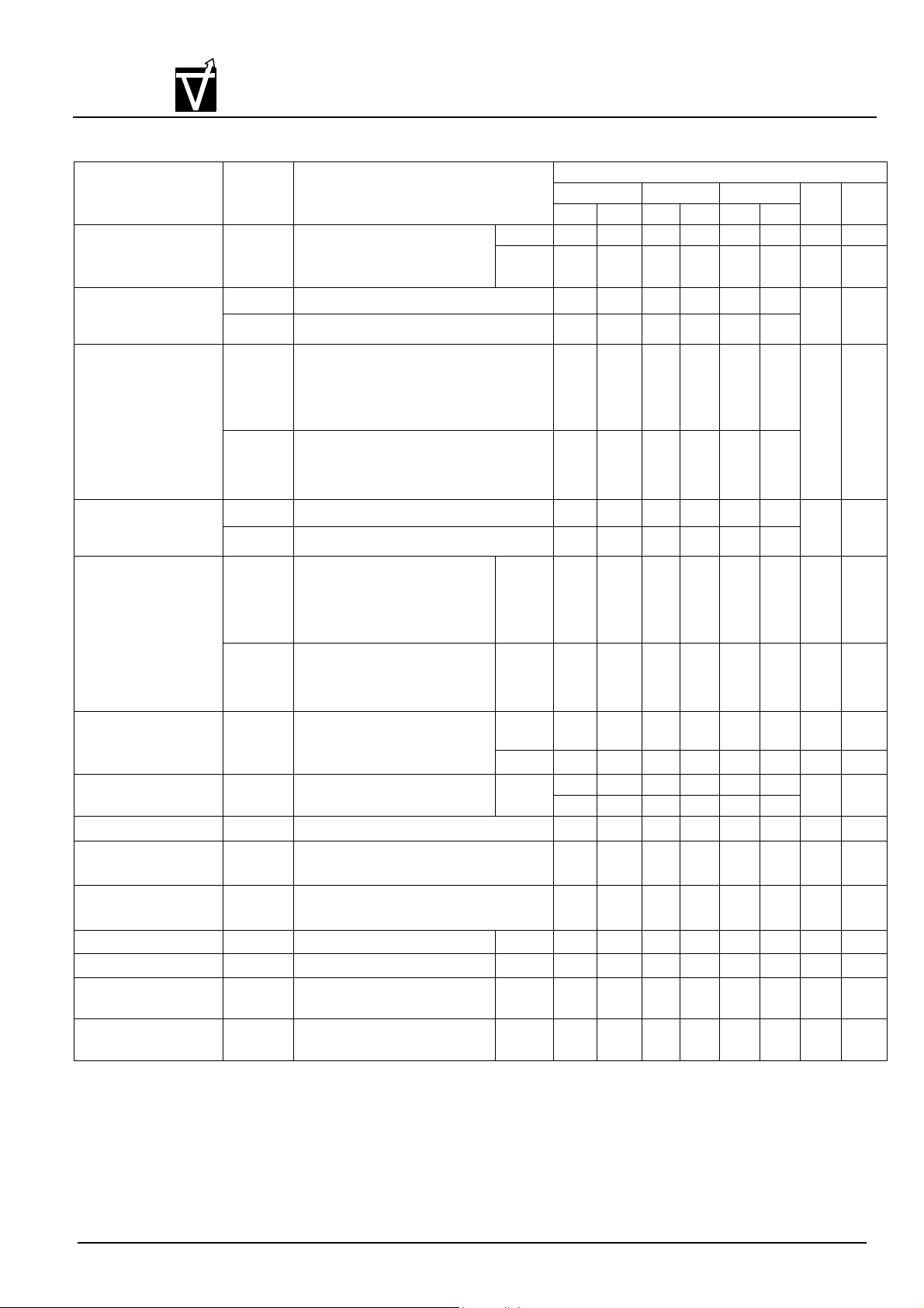
DC Characteristics (Recommended Operating Conditions unless otherwise noted)
Parameter Symbol Test Conditions
Operating current I
Precharge standby
current in power
down mode
Precharge standby
current in Non - power
down mode
Active standby
current in power
down mode
Active standby
current in Nonpower
down mode
Operating current
(Burst mode)
Refresh current I
Selfrefresh current I
lnput Ieakege current I
Output Ieakege
current
Output Low Voltage V
Output High Voltage V
Output Low Voltage V
Output High Voltage V
Notes : 1. ICC1 depends on output loading and cycle rates. Specified values are obtained with the output open.
In addition to this, ICC1 is measured on condition that addresses are changed only one time duringt
2. ICC4 depends on output loading and cycle rates. Specified values are obtained with the output open.
In addition to this, ICC4 is measured on condition that addresses are changed only one time during t
3. ICC5 is measured on condition that addresses are changed only one time during t
4. For LVTTL compatible, VG3664321(4)1.
5. For SSTL - 3 interface, VG3664321(4)2.
6. Refresh on every 15.6s.
CMOS Synchronous Dynamic RAM
VG36648041(2)B
-8H -8L -10 Unit Notes
Min Max Min Max Min Max
CC1
Burst length = 1
One bank active
tRC t
I
CC 2P CKE V
I
CC 2PS
I
CC 2N CKE V
CKE V
CS V
changed one
time during 2 CLK cycles.
I
CC 2NS
CKEV
CLKV
Input signals are stable.
I
CC 3P
I
CC 3PS
I
CC 3N
CKE V
CKE V
CKE V
CS V
Input signals are changed
one time during 2CLKs.
I
CC 3NS CKE V
CLE V
Input signals are stable.
I
CC4
tCK t
Io = 0mA
All banks Active
CC5
CC6
LI
tRC = t
CKE 0.2V
Vin 0, Vin VDD + 0.3V
Pins not under test = 0V
I
LO
V
0, V
out
DQ# in H - Z., Dout disabled
OL
OH
OL
OH
lOL = 2mA 0.4 0.4 0.4 V 4
lOH = -2mA 2.4 2.4 2.4 V 4
l
= 16mA V
OL
lOH = -16mA V
RC(MIN.)
IH(MAX.) tCK
IH(MAX.) tCK
IH(MIN.) tCK
IH(MIN.)
IH(MIN.)
IL(MAX.)
IL(MAX.)
IL(MAX.)
IH(MIN.)
IH(MIN.)
IH(MIN.) tCK
IL(MAX.)
CK(MIN.)
RC(MIN.)
VDD
out
, Io = 0mA
= 15ns
=
= 15ns
Input signals are
, tCK =
, t
= 15ns
CK
, t
=
CK
, t
= 15ns
CK
=
(MAX)
CL = 3 100 100 90 mA 1
CL = 2 95 95 85
3 3 3 mA
2 2 2
20 20 20 mA
6 6 6
5 5 5 mA
4 4 4
25 25 25 mA
10 10 10
CL = 3 160 160 135 mA 2
CL = 2 145 125 105
CL = 3
CL = 2
130 130 110 mA 3,6
125 125 105
2 2 2 mA
- 5 5 - 5 5 - 5 5 uA
- 5 5 - 5 5 - 5 5 uA
TT
+ 0.8
TT
+ 0.8
V
TT
+ 0.8
V
TT
+ 0.8
CK(MIN.)
V
TT
+ 0.8
.
V
TT
+ 0.8
V 5
V 5
CK(MIN.)
CK(MIN.)
.
.
Document : 1G5-0099 Rev.1 Page 6
Page 7
VIS
±
Preliminary VG3664321(4)1(2)BT
CMOS Synchronous Dynamic RAM
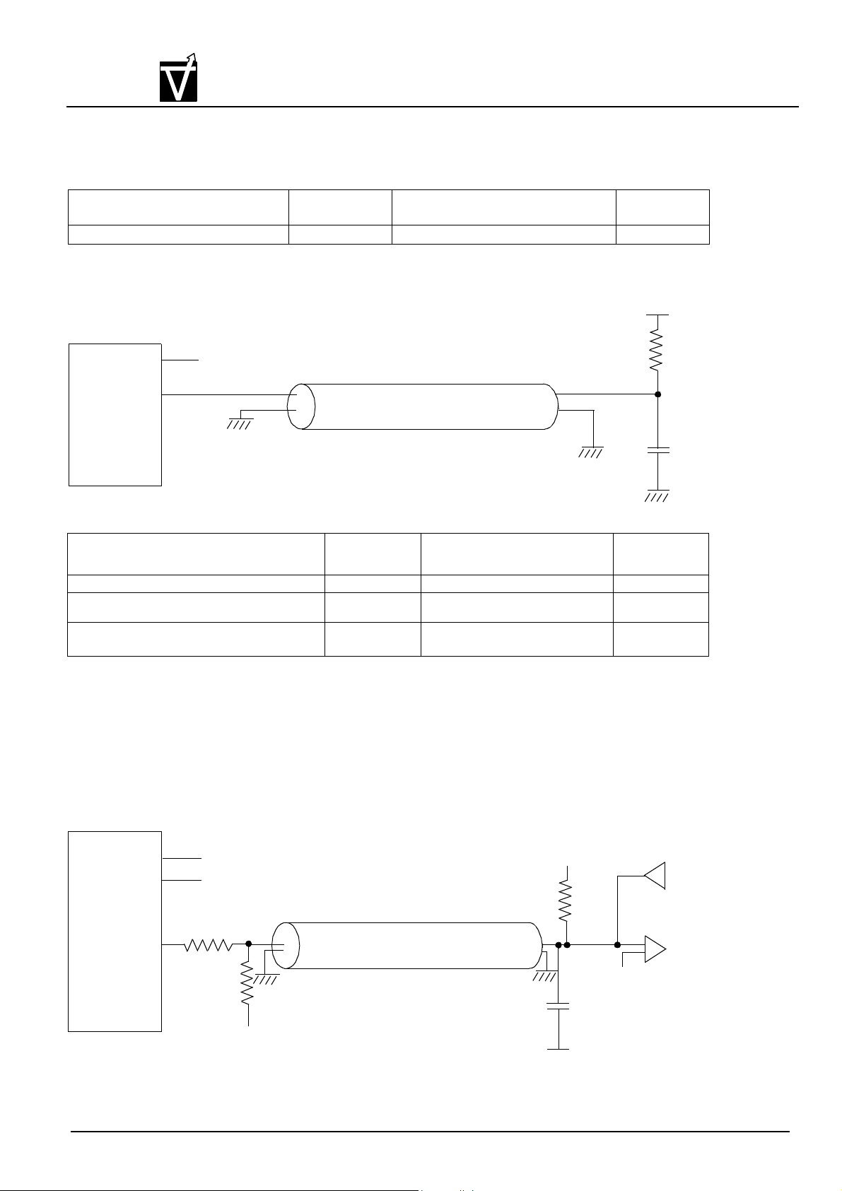
A. C Characteristics : (Ta = 0 to 70°C V
Test Conditions for LVTTL Compatible :
AC input Levels (VIH/VIL) 2.0/0.8V Input timing reference level/
= 3.3V 0.3V
DD
SS
= 0V)
1.4V
Output timing reference level
Input rise and fall time 1ns Output load condition 50pF
AC Test Load Circuits (for LVTTL interface) :
V
DDQ
Device
Under
Test
V
V
DDQ
OUT
Z = 50
Ω
1.4V
50
50PF
Test Conditions for SSTL - 3 Interface
Input Hihg (min)/Input low (max) Voltage VREF + 0.4V/
VREF - 0.4V
Input Reference Voltage
(VREF)
0.45 x VDDQ
Timing Reference Levels of Output Signals 0.45 x VDDQ Input Signal MAX. Slew Rate 1V/ns
Input Signal MAX. Peak to Peak Swing 2.0V Output Circuit See Figure
Below
Min. Required output pull - up under AC
test load
VTT + 0.8V Min. Required output pull -
down under AC test load
VTT - 0.8V
Ω
AC Test Load Circuits (for SSTL - 3 interface) :
V
DDQ
V
REF
V
OUT
Device
Under
Test
Document : 1G5-0099 Rev.1 Page 7
V
DDQ
0.45 * V
RS = 25Ohms
VTT = 0.45 * V
DDQ
RT1 = 50 Ohms
DDQ
Z = 50 Ohms
RT2 = 50 Ohms
C
LOAD
VTT = 0.45 * V
= 30 pF
DDQ
VIN
V
= 0.45 * V
REF
V
SS
DD
Page 8
±
≤
Preliminary VG3664321(4)1(2)BT
VIS
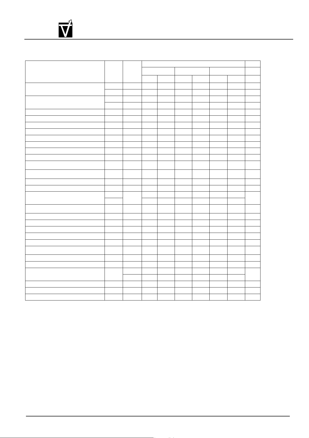
A.C Characteristics : (Ta = 0 to 70°C VDD = 3.3V 0.3V, VSS = 0V)
CMOS Synchronous Dynamic RAM
Parameter CAS
CLK cycle time
Latency
(1)
symbol
3 t
2 t
CLK to valid output delay 3 t
2 t
CLK high pulse width t
CLK low pulse width t
CKE setup time t
CKE hold time t
Address setup time t
Address hold time t
Command setup time t
Command hold time t
Data input setup time t
Data input hold time t
Output data hold time t
CLK to output in low - Z t
CLK to output in Hi - Z 3 t
2 6 6 6
CLK to output in Hi - Z without load t
Row active to active delay t
RAS to CAS delay t
Row precharge time t
ROW active time t
ROW cycle time t
Last data in to burst stop t
Data - in to ACT(REF) command t
Data - in to precharge t
Transition time t
Mode reg. set cycle t
Self refresh exit time t
Refresh time t
ck3
ck2
Ac3
Ac2
CH
CL
CKS
CKH
AS
AH
CMS
CMH
DS
DH
OH
LZ
HZ
OHN
RRD
RCD
RP
RAS
RC
BDL
DAL
DPL
T
t
T
RSC
SRX
REF
VG3664321 (4) 1 (2) B Unit
-8H -8L -10
Min Max Min Max Min Max
8 8 10 ns
10 12 15 ns
6 6 6 ns
6 6 6 ns
3 3 3 ns
3 3 3 ns
2 2 3 ns
1 1 1 ns
2 2 3 ns
1 1 1 ns
2 2 3 ns
1 1 1 ns
2 2 3 ns
1 1 1 ns
3 3 3 ns
0 0 0 ns
6 6 6 ns
1 1 2 ns
16 16 20 ns
20 20 26 ns
20 20 26 ns
48 120K 48 120K 60 120K ns
70 70 90 ns
1 1 1 CLK
1+ t
RP
1+ t
RP
1+ t
RP
8 8 10 ns
(1)
(2)
1 10 1 10 1 10 ns
0.2 5 0.2 5 0.2 5
2 2 2 CLK
1 1 1 CLK
64 64 64 ms
CLK
Notes : (1) The input clock should be stable and continuous. (jitter 7% * tCK)
Document : 1G5-0099 Rev.1 Page 8
Page 9
Preliminary VG3664321(4)1(2)BT
VIS
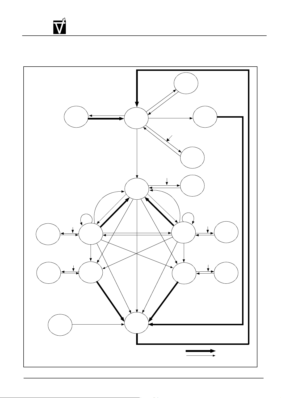
Basic Features and Function description
1. simplified State diagram
CMOS Synchronous Dynamic RAM
Mode
Register
Set
MRS
IDLE
Self
Refresh
y
r
t
n
e
F
L
t
E
S
ACT
i
x
e
F
L
E
S
C
K
REF
CKE
E
AUTO
Refresh
Power
Down
Write (Write recovery)
WRITE
SUSPEND
WRITE A
SUSPEND
CKE
CKE
Write with
Auto Precharge
CKE
CKE
WRITE
WRITE A
B
S
T
READ
READ A
Read
Active
Power
Down
CKE
CKE
Read with
Auto Precharge
CKE
CKE
READ
SUSPEND
READA
SUSPEND
ROW
ACTIVE
T
S
B
h
Write
Write recov
Read (write recovery)
A
u
P
R
E
(
P
t
i
w
ry
h
e
e
t
d
i
r
e
r
W
p
o
t
u
A
R
e
a
d
w
t
o
i
t
P
h
r
e
c
h
a
r
g
r
e
c
h
a
r
g
e
t
e
r
m
i
n
a
t
i
o
n
)
A
e
g
r
a
PRE
Write
W
e
A
(
w
r
i
t
e
P
CKE
CKE
Read
R
u
e
t
a
o
d
P
w
r
e
i
t
c
h
h
a
r
g
e
h
t
i
e
g
w
r
e
a
t
i
r
h
c
e
r
P
o
t
u
r
e
c
o
v
e
r
y
)
)
n
o
i
t
a
n
i
m
r
e
t
e
g
r
a
h
c
e
r
P
(
E
R
POWER
ON
Precharge
Precharge
Automatic sequence
Manual input
Note: After the AUTO refresh operation, precharge operation is
performed automatically and enter the IDLE state
Document : 1G5-0099 Rev.1 Page 9
Page 10
Preliminary VG3664321(4)1(2)BT
VIS
2.Truth Table
2.1 Command Truth Table
FUNCTION Symbol
Device deselect DESL H X H X X X X X X
No operation NOP H X L H H H X X X
Mode register set MRS H X L L L L L L V
Bank activate ACT H X L L H H V V V
Read READ H X L H L H V L V
Read with auto precharge READA H X L H L H V H V
Write WRIT H X L H L L V L V
Write with auto precharge WRITA H X L H L L V H V
Precharge select bank PRE H X L L H L V L X
Precharge all banks PALL H X L L H L X H X
Burst stop BST H X L H H L X X X
CBR (Auto) refresh REF H H L L L H X X X
Self refresh SELF H L L L L H X X X
Notes : (1) Bank address. lt would be different from organizations.
CMOS Synchronous Dynamic RAM
CKE
n - 1 n
CS RAS CAS WE BA
(1)
A10 A9 - A0
2.2 DQM Truth Table
CKE DQM
FUNCTION Symbol
Data write/output enable ENB H X L
Data mask/output disable MASK H X H
DQ24 ~ DQ31 write enable/output enable ENB3 H X L X X X
DQ16 ~ DQ23 write enable/output enable ENB2 H X X L X X
DQ8 ~ DQ7 write enable/output enable ENB1 H X X X L X
DQ0 ~ DQ7 write enable/output enable ENB0 H X X X X L
DQ24 ~ DQ31 write enable/output enable MASK3 H X H X X X
DQ16 ~ DQ23 write enable/output enable MASK2 H X X H X X
DQ8 ~ DQ15 write enable/output enable MASK1 H X X X H X
DQ0 ~ DQ7 write enable/output enable MASK0 H X X X H
2.3 CKE Truth Table
Current State Function Symbol
Activating Clock suspend mode entry H L X X X X X
Any Clock suspend L L X X X X X
Clock suspend Clock suspend mode exit L H X X X X X
Idle CBR refresh command REF H H L L L H X
Idle Self refresh entry SELF H L L L L H X
Self refresh Self refresh exit L H L H H H X
Idle Power down entry H L X X X X X
Power down Power down exit L H X X X X X
H : High level, L : Low level
X : High or Low level (Don’t care), V : Valid Data input
n - 1 n - 1 3 2 1 0
CKE
CS RAS CAS WE
L H H X X X X
Add
ressn - 1 n
Document : 1G5-0099 Rev.1 Page 10
Page 11
VIS
→
→
→
→
→
→
Preliminary VG3664321(4)1(2)BT
CMOS Synchronous Dynamic RAM
2.4 Operative Command Table Notes 1
Current state CS RAS CAS WE Address Command Action Notes
Idle H X X X X DESL Nop or Power down 2
L H H X X NOP or BST Nop or Power down 2
L H L H BA, CA, A10 READ/READA ILLEGAL 3
L H L L BA, CA, A10 WRIT/WRITA ILLEGAL 3
L L H H BR, RA ACT Row active
L L H L BA, A10 PRE/PALL Nop
L L L H X REF/SELF Refresh or Self refresh 4
L L L L Op - Code MPS Mode register access
Row active H X X X X DESL Nop
L H H X X NOP or BST Nop
L H L H BA, CA, A10 READ/READA Begin read : Determine AP 5
L H L L BA, CA, A10 WRIT/WRITA Begin write : Determine AP 5
L L H H BA, RA ACT ILLEGAL 3
L L H L BA, A10 PRE/PALL Precharge 6
L L L H X REF/SELF ILLEGAL
L L L L Op - Code MRS ILLEGAL
Read H X X X X DESL
L H H H X NOP
L H H L X BST
L H L H BA, CA, A10 READ/READA Term burst, new read : Determine AP 7
L H L L BA, CA, A10 WRIT/WRITA Term burst, start write : Determine AP 7,8
L L H H BA, RA ACT ILLEGAL 3
L L H L BA, A10 PRE/PALL Term burst, precharging
L L L H X REF/SELF ILLEGAL
L L L L Op - Code MRS ILLEGAL
Write H X X X X DESL
L H H H X NOP
L H H L X BST
L H L H BA, CA, A10 READ/READA Term burst, start read : Determine AP 7,8
L H L L BA, CA, A10 WRIT/WRITA Term burst, new write : Determine AP 7
L L H H BA, RA ACT ILLEGAL 3
L L H L BA, A10 PRE/PALL Term burst, precharging 9
L L L H X REF/SELF ILLEGAL
L L L L Op - Code MRS ILLEGAL
Continue burst to end Row active
Continue burst to end Row active
Burst stop Row active
Continue burst to end write recovering
Continue burst to end write recovering
Burst stop Row active
(1/3)
Document : 1G5-0099 Rev.1 Page 11
Page 12
→
→
→→→→→→→
→
→
Preliminary VG3664321(4)1(2)BT
VIS
CMOS Synchronous Dynamic RAM
(2/3)
Current state CS RAS CA WE Address Command Action No
Read with auto
precharge
Write with auto
precharge
Precharging H X X X X DESL
Row activating H X X X X DESL
H X X X X DESL
L H H H X NOP
L H H L X BST ILLEGAL
L H L H BA, CA, A10 READ/READA ILLEGAL 11
L H L L BA, CA, A10 WRIT/WRITA ILLEGAL 11
L L H H BA, RA ACT ILLEGAL 3,11
L L H L BA, A10 PRE/PALL ILLEGAL 3,11
L L L H X PEF/SELF ILLEGAL
L L L L Op - Code MRS ILLEGAL
H X X X X DESL
L H H H X NOP
L H H L X BST ILLEGAL
L H L H BA, CA, A10 READ/READA ILLEGAL 11
L H L L BA, CA, A10 WRIT/WRITA ILLEGAL 11
L L H H BA, RA ACT ILLEGAL 3,11
L L H L BA, A10 PRE/PALL ILLEGAL 3,11
L L L H X REF/SELF ILLEGAL
L L L L Op - code MRS ILLEGAL
L H H H X NOP
L H H L X BST
L H L H BA, CA, A10 READ/READA ILLEGAL 3
L H L L BA, CA, A10 WRIT/WRITA ILLEGAL 3
L L H H BA, RA ACT ILLEGAL 3
L L H L BA, A10 PRE/PALL
L L L H X REF/SELF ILLEGAL
L L L L Op - Code MRS ILLEGAL
L H H H X NOP
L H H L X BST
L H L H BA, CA, A10 READ/READA ILLEGAL 3
L H L L BA, CA, A10 WRIT/WRITA ILLEGAL 3
L L H H BA, RA ACT ILLEGAL 3,9
L L H L BA, A10 PRE/PALL ILLEGAL 3
L L L H X REF/SELF ILLEGAL
L L L L Op - Code MRS ILLEGAL
Continue burst to end Precharging
Continue burst to end Precharging
Continue burst to end write
recovering with auto precharge
Continue burst to end write
recovering with auto precharge
Nop Enter idle after t
Nop Enter idle after t
Nop Enter idle after t
Nop Enter idle after t
Nop Enter row active after t
Nop Enter row active after t
Nop Enter row active after t
RP
RP
RP
RP
RCD
RCD
RCD
Document : 1G5-0099 Rev.1 Page 12
Page 13
→→→
→
→
→
→
→
Preliminary VG3664321(4)1(2)BT
VIS
Current state CS RAS CA WE Address Command Action Notes
Write
recovering
Write
recovering
with auto
precharge
Auto
Refreshing
Mode register
accessing
Note 1. All entries assume that CKE was active (High level) during the preceding clock cycle.
2. If both banks are idle, and CKE is inactive (Low level), the device will enter Power down mode.
All input buffers except CKE will be disabled.
3. Illegal to bank in specified states; Function may be legal in the bank indicated by Bank Address
(BA), depending on the state of that bank.
4. If both banks are idle, and CKE is inactive (Low level), the device will enter Self refresh mode.All
input buffers except CKE will be disabled.
5. Illegal if t
6. Illegal if t
7. Must satisfy burst interrupt condition.
8. Must satisfy bus contention, bus turn around, and/or write recovery requirements.
9. Must mask preceding data which don’t satisfy t
10. Illegal if t
11. Illegal for single bank, but legnl for other banks in mulfi - bank deuleo.
CMOS Synchronous Dynamic RAM
(3/3)
H X X X X DESL
L H H H X NOP
L H H L X BST
L H L H BA, CA, A10 READ/READA Start read, Determine AP 8
L H L L BA, CA, A10 WRIT/WRITA New write, Determine AP
L L H H BA, RA ACT ILLEGAL 3
L L H L BA, A10 PRE/PALL ILLEGAL 3
L L L H X PEF/SELF ILLEGAL
L L L L Op - Code MRS ILLEGAL
H X X X X DESL
L H H H X NOP
L H H L X BST
L H L H BA, CA, A10 READ/READA ILLEGAL 3,8,11
L H L L BA, CA, A10 WRIT/WRITA ILLEGAL 3,11
L L H H BA, RA ACT ILLEGAL 3,11
L L H L BA, A10 REF/PALL ILLEGAL 3
L L L H X REF/SELF ILLEGAL
L L L L Op - Code MRS ILLEGAL
H X X X X DESL Nop Enter idle after t
L H H X X NOP/BST Nop Enter idle after t
L H L X X READ/WRIT ILLEGAL
L L H X X ACT/PRE/PALL ILLEGAL
L L L X X REF/SELF/MRS ILLEGAL
H X X X X DESL
L H H H X NOP
L H H L X BST ILLEGAL
L H L X X READ/WRITE ILLEGAL
L L X X X ACT/PRE/PALL/
REF/SELF/MRS
is not satisfied.
RCD
is not satisfied.
RAS
.
DPL
is not satisfied.
RRD
Nop Enter row active after t
Nop Enter row active after t
Nop Enter row active after t
Nop Enter precharge after t
Nop Enter precharge after t
Nop Enter precharge after t
RC
RC
Nop Enter idle after 2 Clocks
Nop Enter idle after 2 Clocks
ILLEGAL
DPL
DPL
DPL
DPL
DPL
DPL
Document : 1G5-0099 Rev.1 Page 13
Page 14
VIS
→
Preliminary VG3664321(4)1(2)BT
CMOS Synchronous Dynamic RAM
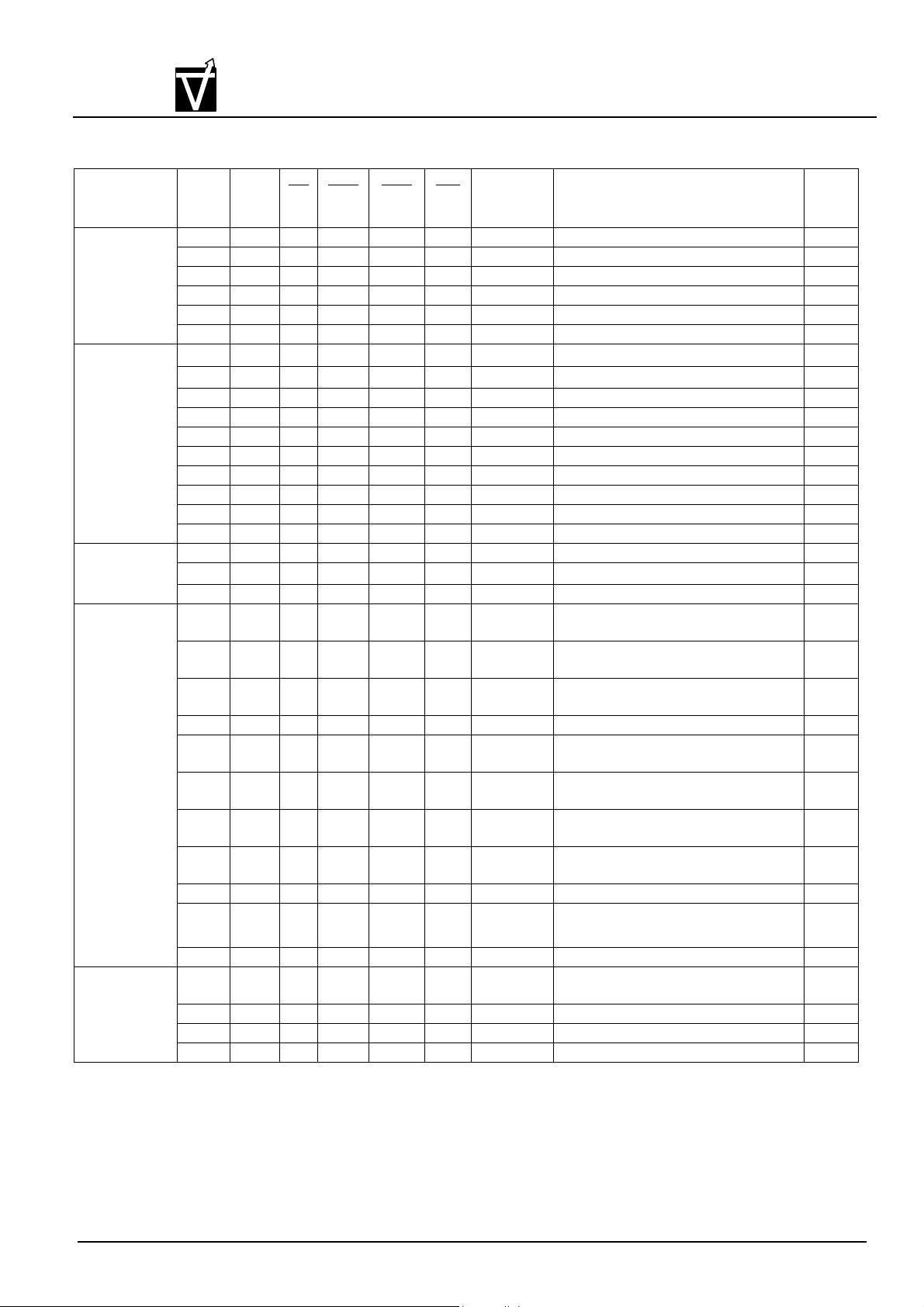
2.5 Command Truth Table for CKE
Current state CKE
n - 1
Self refresh
(S.R.)
Self refresh
recovery
Power down
(P.D.)
Both banks idle H H H X X X Refer to operations in Operative
Any state other
than listed
above
Note 1. H : Hight level, L : low level, X : High or low level (Don't care).
2. CKE Low to High transition will re - enable CLK and other inputs asynchronously. A minimum setup time
must be satisfied before any command other than EXIT.
3. Power down and Self refresh can be entered only from the both banks idle state.
4. Must be legal command as defined in Operative Command Table.
5. Illegal if t
SREX
CKEnCS RAS CAS WE Address Action Notes
H X X X X X X INVALID, CLK (n - 1)would exit S.R.
L H H X X X X S.R. Recovery 2
L H L H H X X S.R. Recovery 2
L H L H L X X ILLEGAL
L H L L X X X ILLEGAL
L L X X X X X Maintain S.R.
H H H X X X X Idle after t
H H L H H X X Idle after t
H H L H L X X ILLEGAL
H H L L X X X ILLEGAL
H L H X X X X Begin clock suspend next cycle 5
H L L H H X X Begin clock suspend next cycle 5
H L L H L X X ILLEGAL
H L L L X X X ILLEGAL
L H X X X X X Exit clock suspend next cycle 2
L L X X X X X Maintain clock suspend
H X X X X X INVALID, CLK (n - 1) would exit P.D.
L H X X X X X
L L X X X X X Maintain power down mode
H H L H X X Refer to operations in Operative
H H L L H X Refer to operation in Operative
H H L L L H X Auto Refresh
H H L L L L Op - Code Refer to operations in Operative
H L H X X X Refer to operations in Operative
H L L H X X Refer to operations in Operative
H L L L H X Refer to operations in Operative
H L L L L H X Self refresh 3
H L L L L L Op - Code Refer to operations in Operative
L X X X X X X Power down 3
H H X X X X X Refer to operations in Operative
H L X X X X X Begin clock suspend next cycle 4
L H X X X X X Exit clock suspend next cycle
L L X X X X X Maintain clock suspend
is not satisfied.
Note 1
RC
RC
EXIT P.D. Idle
Command Table
Command Table
Command Table
Command Table
Command Table
Command Table
Command Table
Command Table
Command Table
2
Document : 1G5-0099 Rev.1 Page 14
Page 15
Preliminary VG3664321(4)1(2)BT
VIS
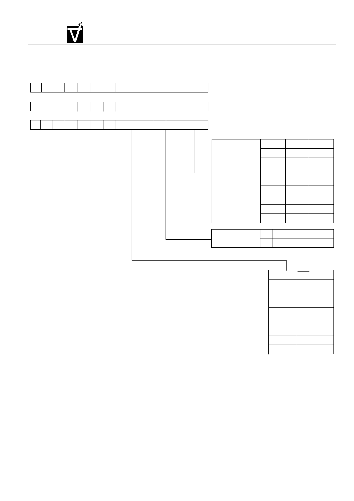
5.Mode Register (Address Input for Mode Set)
CMOS Synchronous Dynamic RAM
13
12
0 Reserved
0
12
13
x
x
13
12
x
x
10
11
0 0
11 10
x
x
11
10
x x 0
9 8
0 0
9
1
9
8
0
8
0 0
7
1
7 6
0
7 6
6
5
5
LTMODE
5
LTMODE
3
4
3 2
4
WT
3
4
WT
2 1
2
1
BL
1
BL
0
JEDEC Standard Test Set
0
Burst Read and Single Write (for Write Through Cache)
0
Burst Read and Burst Write X = Don’t care
Burst length
Wrap type
Bits2 - 0
000
001
010
011
100
101
110
111
0
1
WT = 0
1
2
4
8
R
R
R
Full page
Sequential
Interleave
WT = 1
1
2
4
8
R
R
R
R
Latency
mode
Bits6 - 4
000
001
010
011
100
101
110
111
Remark R : Reserved
CAS Iatency
R
R
2
3
R
R
R
R
Document : 1G5-0099 Rev.1 Page 15
Page 16
Preliminary VG3664321(4)1(2)BT
VIS
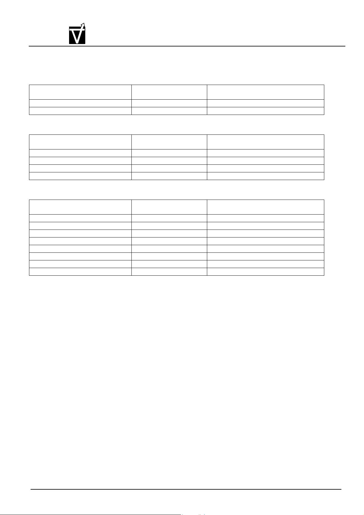
5.1 Burst Length and Sequence
(Burst of Two)
Starting Address
(column address A0, binary)
(Burst of Four)
Starting Address
(column address A1 - A0, binary)
(Burst of Eight)
Starting Address
(column address A2 - A0, binary)
CMOS Synchronous Dynamic RAM
0 0, 1 0, 1
1 1, 0 1, 0
00 0, 1, 2, 3 0, 1, 2, 3
01 1, 2, 3, 0 1, 0, 3, 2
10 2, 3, 0, 1 2, 3, 0, 1
11 3, 0, 1, 2 3, 2, 1, 0
000 0, 1, 2, 3, 4, 5, 6, 7 0, 1, 2, 3, 4, 5, 6, 7
001 1, 2, 3, 4, 5, 6, 7, 0 1, 0, 3, 2, 5, 4, 7, 6
010 2, 3, 4, 5, 6, 7, 0, 1 2, 3, 0, 1, 6, 7, 4, 5
011 3, 4, 5, 6, 7, 0, 1 ,2 3, 2, 1, 0, 7, 6, 5, 4
100 4, 5, 6, 7, 0, 1, 2, 3 4, 5, 6, 7, 0, 1, 2, 3
101 5, 6 ,7, 0, 1, 2, 3, 4 5, 4, 7, 6, 1, 0, 3, 2
110 6, 7 ,0 ,1 ,2 ,3 ,4 ,5 6, 7, 4, 5, 2, 3, 0, 1
111 7, 0, 1, 2, 3, 4, 5, 6 7, 6, 5, 4, 3, 2, 1, 0
Sequential Addressing
Sequence (decimal)
Sequential Addressing
Sequence (decimal)
Sequential Addressing
Sequence (decimal)
Interleave Addressing Sequence (decimal)
Interleave Addressing Sequence (decimal)
Interleave Addressing Sequence(decimal)
Full page burst is an extension of the above tables of sequential addressing, with the length
being 256 for 4B 2M x 32, and 512 for 2B 2M x 32.
Document : 1G5-0099 Rev.1 Page 16
Page 17
Preliminary VG3664321(4)1(2)BT
VIS
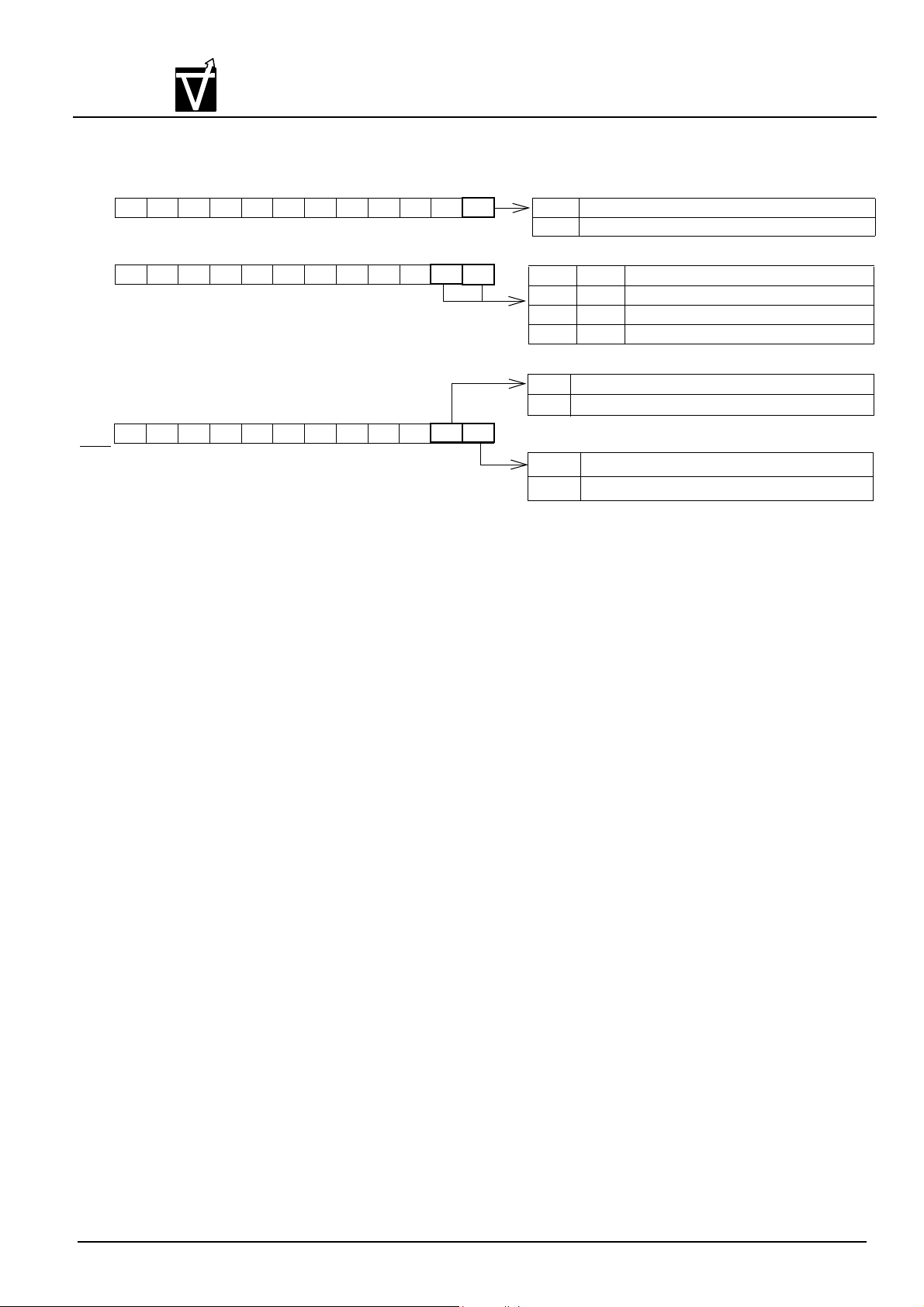
6.Address Bits of Bank-Select and Precharge
6.1 Qual banks controlled by A11 (for VG36643211/VG36643212)
CMOS Synchronous Dynamic RAM
Row
A0 A1 A2 A3 A4 A5 A6 A7 A8 A9 A10 A11
(Activate command)
A0 A1 A2 A3 A4 A5 A6 A7 A8 A9 A10 A11
Row
(Activate command)
A0 A1 A2 A3 A4 A5 A6 A7 A8 A9 A10 A11
Co1.
(CAS strobes)
0 Select Bank A “Activate” command
1 Select Bank B “Activate” command
A10 A11 Result
0 0 Precharge Bank A
0 1 Precharge Bank B
1 X Precharge All Banks
X : Don’t care
0 disables Auto - Precharge (End of Burst)
1 Enables Auto - Precharge (End of Burst)
0 enables Read / Write commands for Bank B
1 enables Read / Write commands for Bank B
Document : 1G5-0099 Rev.1 Page 17
Page 18
Preliminary VG3664321(4)1(2)BT
VIS
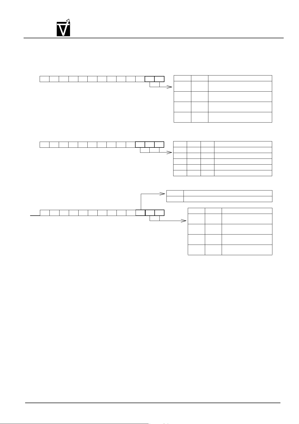
6.2 Quad banks controlled by A11 & A12 (for VG36643241 / VG36643242)
CMOS Synchronous Dynamic RAM
A0 A1 A2 A3 A4 A5 A6 A7 A8 A9 A10A11 A12
Row
(Activate command)
A0 A1 A2 A3 A4 A5 A6 A7 A8 A9 A10A11 A12
Row
(Precharge command)
A0 A1 A2 A3 A4 A5 A6 A7 A8 A9 A10A11 A12
Col.
(CAS strobes)
A11 A12 Result
0 0 Select Bank A
“Activate” command
0 1 Select Bank B
“Activate” command
1 0 Select Bank C
“Activate” command
1 1 Select Bank D
“Activate” command
A10 A11 A12 Result
0 0 0 Precharge Bank A
0 0 1 Precharge Bank B
0 1 0 Precharge Bank C
0 1 1 Precharge Bank D
1 x x Precharge AII Banks
X : Don’t care
0 Disables Auto - Precharge (End of Burst)
1 Enables Auto - Precharge (End of Burst)
A11 A12 Result
0 0 Enables Read / Write
commants for Baml A
0 1 Enables Read / Write
commants for Baml B
1 0 Enables Read / Write
commants for Baml C
1 1 Enables Read / Write
commants for Baml D
Document : 1G5-0099 Rev.1 Page 18
Page 19
VIS
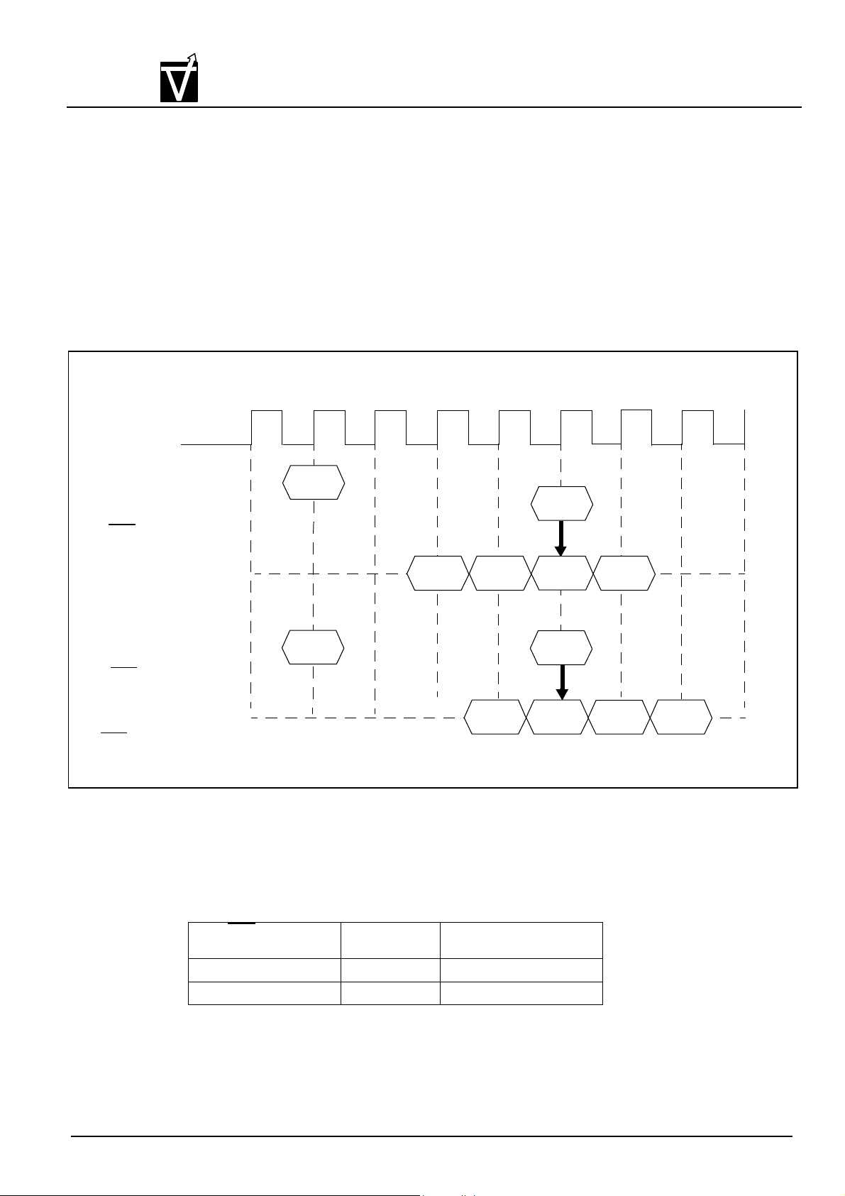
7.PRECHARGE
Preliminary VG3664321(4)1(2)BT
CMOS Synchronous Dynamic RAM
synchronous DRAM enters the idle state after t
required to perform the precharge.
any data in the burst is as follows.
PRECHARGE
CLK
Command
CAS latency = 2
DQ
The precharge command can be asserted anytime after t
Soon after the precharge command is asserted, the precharge operation is performed and the
is satisfied. The parameter tRP is the time
RP(min.)
The earliest timing in a read cycle that a precharge command can be asserted without losing
T0 T1
Read
T2
Q0
RAS(min)
T3
Q1
is satisfied.
T4 T5
PRE
Burst length = 4
T6
Q3Q2
T7
Hi - Z_
Command
CAS latency = 3
DQ
CAS latency = 2 : One clock earlier than the last output data.
3 : Two clocks earlier than the last output data.
4 : Three clocks earlier than the last output data.
In order to write all data to the memory cell correctly, the asynchronous parameter ”t
be satisfied. The t
asserted. The minimum number of clocks are calculated by dividing t
time.
In summary, the precharge command can be asserted relative to reference clock that indicates the last data word is valid. In following table, minus means clocks before the reference; plus
means time after the reference.
DPL(min.)
CAS latency Read
Read
specification defines the earliest time that a precharge command can be
2 -1 + t
3 -2 + t
Q0
Write
DPL(min.)
DPL(min.)
PRE
Q1
DPL(min.)
Q2
by the clock cycle
Q3
(t
RAS is satisfied
” must
DPL
Hi - Z
)
Document : 1G5-0099 Rev.1 Page 19
Page 20
Preliminary VG3664321(4)1(2)BT
VIS
8.Auto Precharge
During a read or write command cycle, A10 controls whether auto precharge is selected.
If A10 is high in the read or write command (Read with Auto precharge command or Write with
Auto precharge command), auto precharge is selected and precharging begins automatically
after the burst access.
In the write cycle, t
to the bank being precharged.
When using auto precharge in the read cycle, knowing when the precharge starts is
important because the next activate command to the bank being precharged cannot be executed until the precharge cycle ends. Once auto precharge has started, an activate command
to the bank can be asserted after tRP has been satisfied.
A Read or Write command without auto - precharge can be terminated in the midst of a
burst operation. However, a Read or Write command with auto - precharge can not be interrupted by the same bank commands before the entire burst operation is completed. Therefore
use of the same bank Read, Write, Precharge or Burst Stop command is prohibited during a
read or write cycle with auto - precharge. It should be noted that the device will not respond to
the Auto - Precharge command if the device is programmed for full page burst read or write
cycles.
The timing when the auto precharge cycle begins depends both on both the CAS Iatency
programmed into the mode register and whether the cycle is read or write.
CMOS Synchronous Dynamic RAM
DAL(min.)
must be satisfied before asserting the next activate command
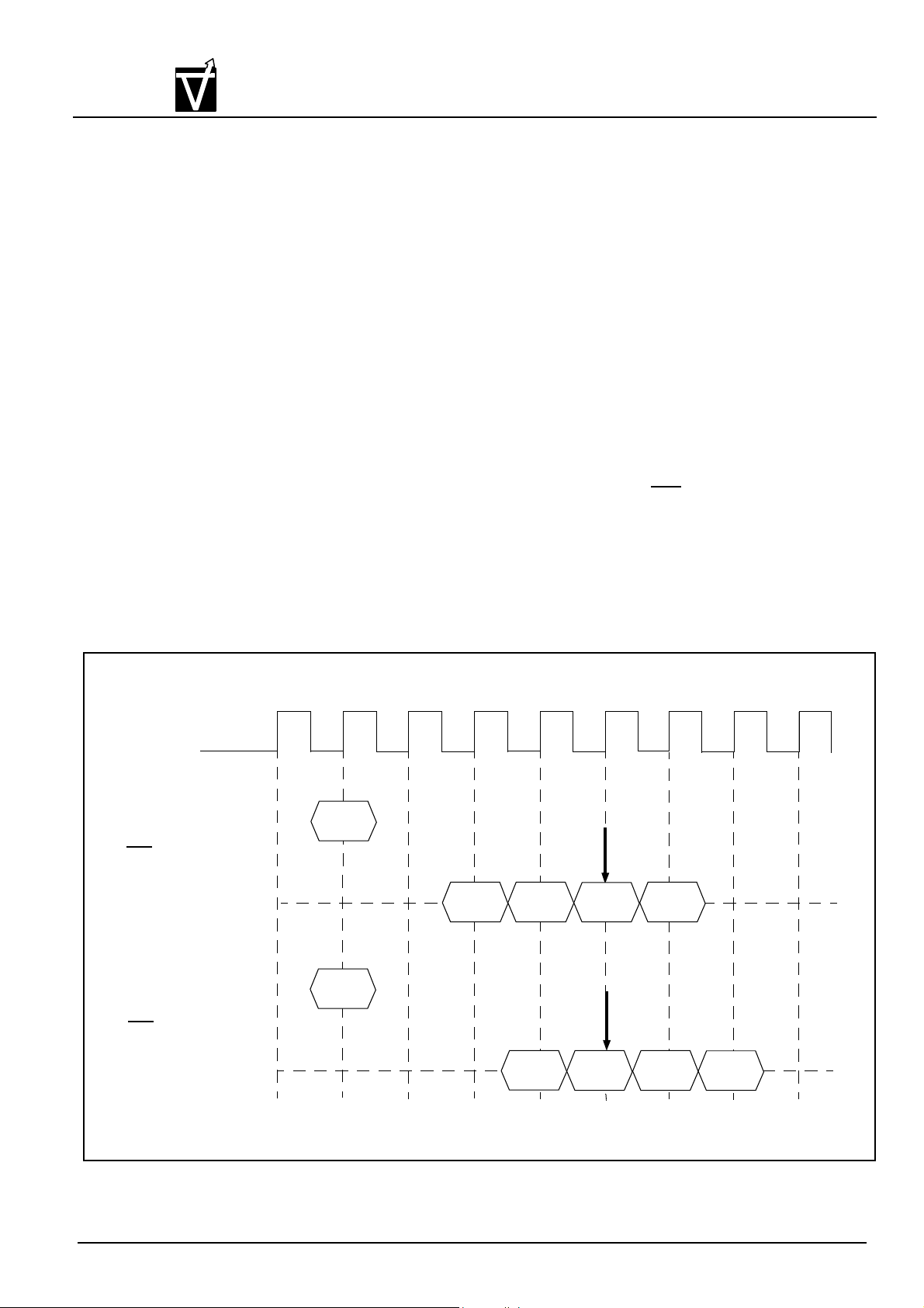
8.1 Read with Auto Precharge
During a READA cycle, the auto precharge begins one clock earlier (CL = 2) or two
clocks earlier (CL = 3) than the last word output.
READ with AUTO PRECHARGE
T0 T1
CLK
Command
READA B
CAS latency = 2
DQ
Command
READA B
T2
QB0
T3
T4
Auto precharge starts
QB1
Auto precharge starts
T5
Burst length = 4
T6
QB3QB2
T7
Hi - Z
T8
CAS latency = 3
DQ
Remark READA means READ with AUTO PRECHARGE
Document : 1G5-0099 Rev.1 Page 20
QB0
QB1
QB2
QB3
Hi - Z
Page 21
Preliminary VG3664321(4)1(2)BT
VIS
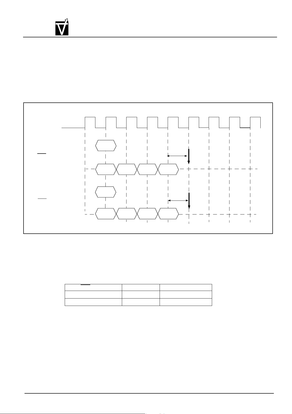
8.2 Write with Auto Precharge
of t
WRITE with AUTO PRECHRGE
CLK
CMOS Synchronous Dynamic RAM
During a write cycle, the auto precharge starts at the timing that is equal to the value
DPL(min.)
after the last data word input to the device.
T0 T1
Burst length = 4
T
2
T3
T4 T5
T6
T7
T8
Command
WRITA B
CAS latency = 2
DQ
Command
CAS latency = 3
DQ
Remark WRITA means WRITE with Auto precharge
In summary, the auto precharge cycle begins relative to a reference clock
that indicates the last data word is valid.
In the table below, minus means clocks before the reference; plus means
clocks after the reference.
CAS latency Read Write
DB0
WRITA B
DB0
2 -1 + t
3 -2 + t
DB1
DB1
DB2
AUTO PRECHARGE starts
t
DPL
DB3DB2
AUTO PRECHARGE starts
t
DPL
DB3
DPL(min.)
DPL(min.)
Hi - Z
Hi - Z
_
Document : 1G5-0099 Rev.1 Page 21
Page 22
VIS
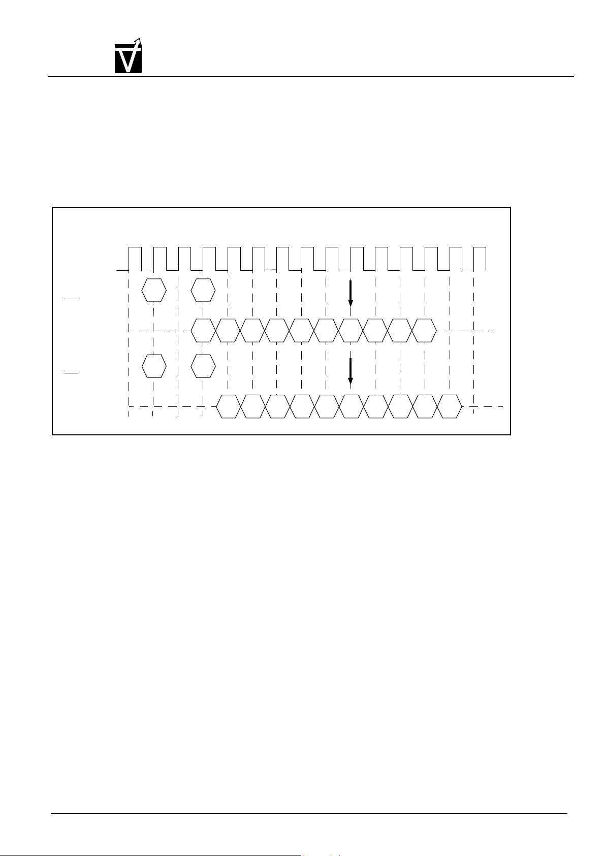
8.3 Multidank Operation - Read with Auto Precharge
Multibank Operation
CLK
Command
CAS latency=2
Preliminary VG3664321(4)1(2)BT
CMOS Synchronous Dynamic RAM
During a READA cycle interrupted by a Read. Write command of
another banks, the auto - precharge scheduled time would not be changed.
T0 T1 T2 T3 T4 T5 T6 T7 T8 T9 T10 T11 T12 T13 T14
Auto precharge bank A starts
READA A
Read B
Burst lengh=8
DQ
Command
CAS latency=3
DQ
READA A
QA0
Read B
QA1
QB0
QA0 QA1
similiar top. 21
QB2 QB3 QB4 QB5 QB6 QB7 QB1
Auto precharge bank A starts
QB0 QB2
QB3
QB4
Hi-Z
QB5 QB6 QB7 QB1
Hi-Z
Document : 1G5-0099 Rev.1 Page 22
Page 23
Preliminary VG3664321(4)1(2)BT
VIS
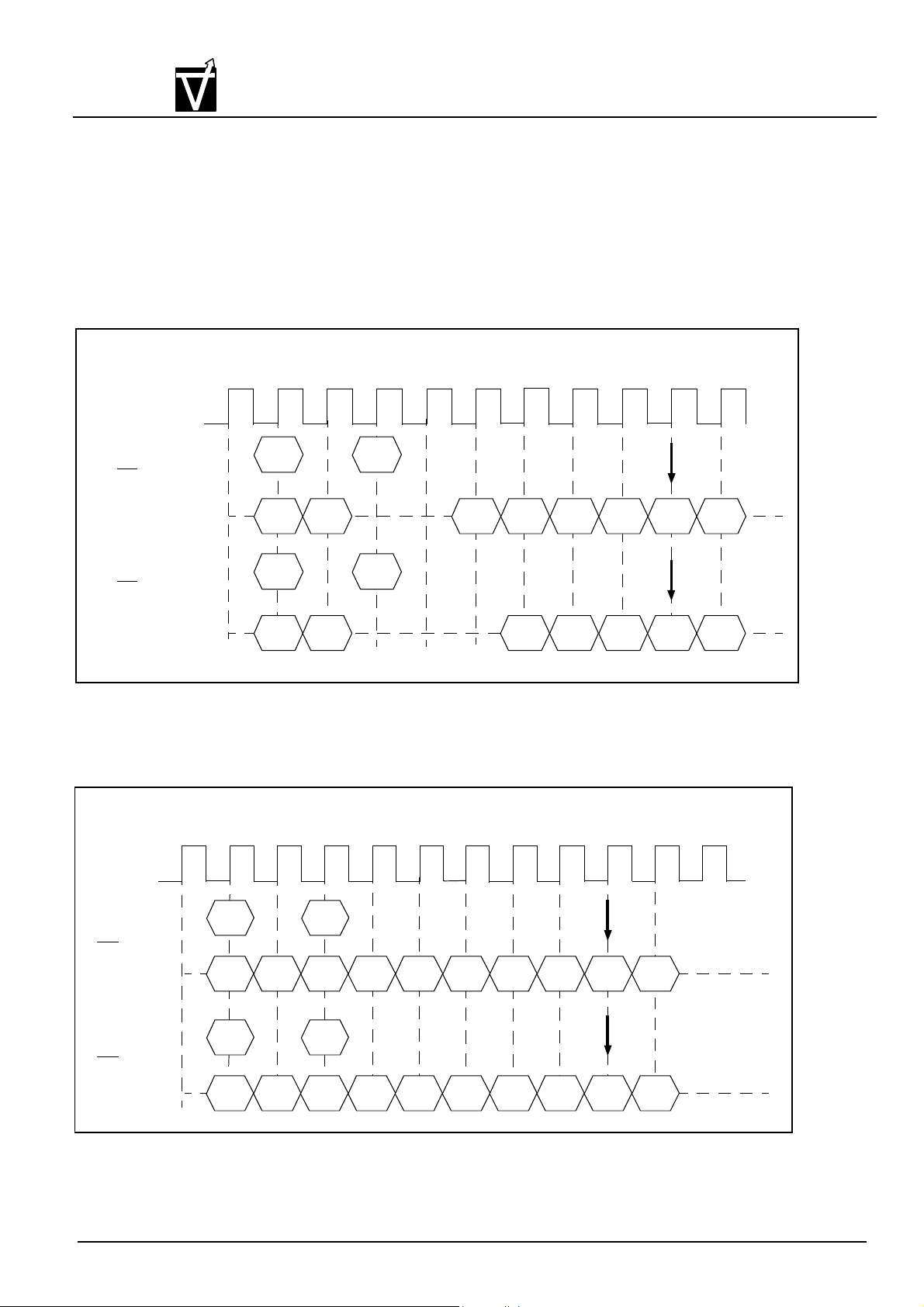
8.3 Multidank Operation - Write with Auto Precharge
During a WRITEA cycle interrupted by a Read, Write command of another banks, the
auto - precharge scheduled time would not be changed.
Multidank Operation
CLK
Command
CAS latency=2
CMOS Synchronous Dynamic RAM
T0 T1 T2 T3 T4 T5 T6 T7 T8 T9 T10
WRITA A
Read B
Burst length = 8
Auto precharge bank A starts
DQ
Command
CAS latency=3
DQ
Multibank Operation
T0 T1 T2 T3 T4 T5 T6 T7 T8 T9 T10 T11
CLK
Command
CAS latency=2
DQ
DA0
WRITA A
DA0
WRITA A Write B
DA0
DA1
DA1
DA1
DB0
Read B
DB1 DB2
DB3
DB0
DB1
DB0
DB4 DB6
DB2 DB3
DB1
Auto precharge bank A starts
DB5
Auto precharge bank A starts
DB2 DB3
DB4
Auto precharge bank A starts
DB7
DB5
DB4
Burst length = 8
Hi-Z
Hi-Z
Hi-Z
DA1
Write B
DB0
DB1 DB2
DB3
DB4 DB5 DB6
DB7
Command
CAS latency=3
DQ
WRITA A
DA0
Document : 1G5-0099 Rev.1 Page 23
Hi-Z
Page 24
Preliminary VG3664321(4)1(2)BT
VIS
9.READ/WRITE Command Interval
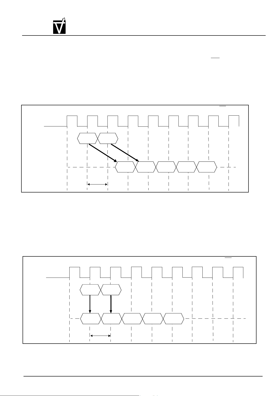
9.1 Read to Read command interval
During a read cycle when a new read command is asserted, it will be effective after the CAS
latency, even if the previous read operation has not completed. READ will be interrupted by another
READ.
Each read command can be asserted in every clock without any restriction.
READ to READ Command Interval
CLK
CMOS Synchronous Dynamic RAM
T0 T1
T2
T3
T4 T5
Burst lengh=4, CAS latency=2
T6
T7
T8
1 cycle
Read B
QB0
QB2QB1
Command
DQ QA0
Read A
9.2 WRITE to WRITE Command Interval
During a write cycle, when a new Write command is asserted, the previous burst will terminated
and the new burst will begin with a new write command. WRITE will be interrupted by another
WRITE.
Each write command can be asserted in every clock without any restriction.
WRITE to WRITE Command Interval
T0 T1
T2
T3
T4 T5
QB3
Burst lengh=4, CAS latency=2
T6
Hi-Z_
T7
T8
CLK
1 cycle
Write B
QB0
QB2QB1
QB3
Hi-Z_
Command
DQ
Write A
QA0
Document : 1G5-0099 Rev.1 Page 24
Page 25
Preliminary VG3664321(4)1(2)BT
VIS
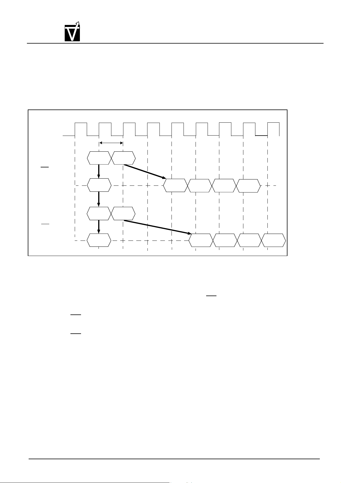
9.3 Write to Read Command lnterval
The write command to read command to read command interval is also a minimum of 1 cycle. Only the
write data before the read command will be written. The data bus must be Hi - Z at least one cycle prior to
the first D
OUT
CLK
CMOS Synchronous Dynamic RAM
.
Burst length = 4
T0 T1
1 cycle
T2
T3
T4 T5
T6
T7
T8
Command
CAS latency=2
DQ
Command
CAS latency=3
DQ
WRITE A
DA0
Write A
DA0
9.4 Read to Write command lnterval
During READ cycle, READ can be interrupted by WRITE. When the CAS latency is 3
and the burst length is Full page, the burst read cannot be interrupted by WRITE (A Burst
Stop command (BST) or a - Precharge command can interrupt).
In case CAS latency is 2, the read and write command interval is 1 cycle minimum.
The data bus must be Hi - Z using DQM before WRITE and DQM must be High at least 3
clocks prior to the Write command. There is a restriction to avoid data conflict.
In case CAS latency is 3 (bust length is not Full page), READ can be interrupted by
WRITE command. The minimum command interval is [burst length + 1] cycles. DQM
must be High at least 3 clocks prior to the Write command.
Read B
Read B
Hi-Z
Hi-Z
QB0
QB1
QB0
QB1
QB3QB2
QB2
QB3
Document : 1G5-0099 Rev.1 Page 25
Page 26
Preliminary VG3664321(4)1(2)BT
VIS
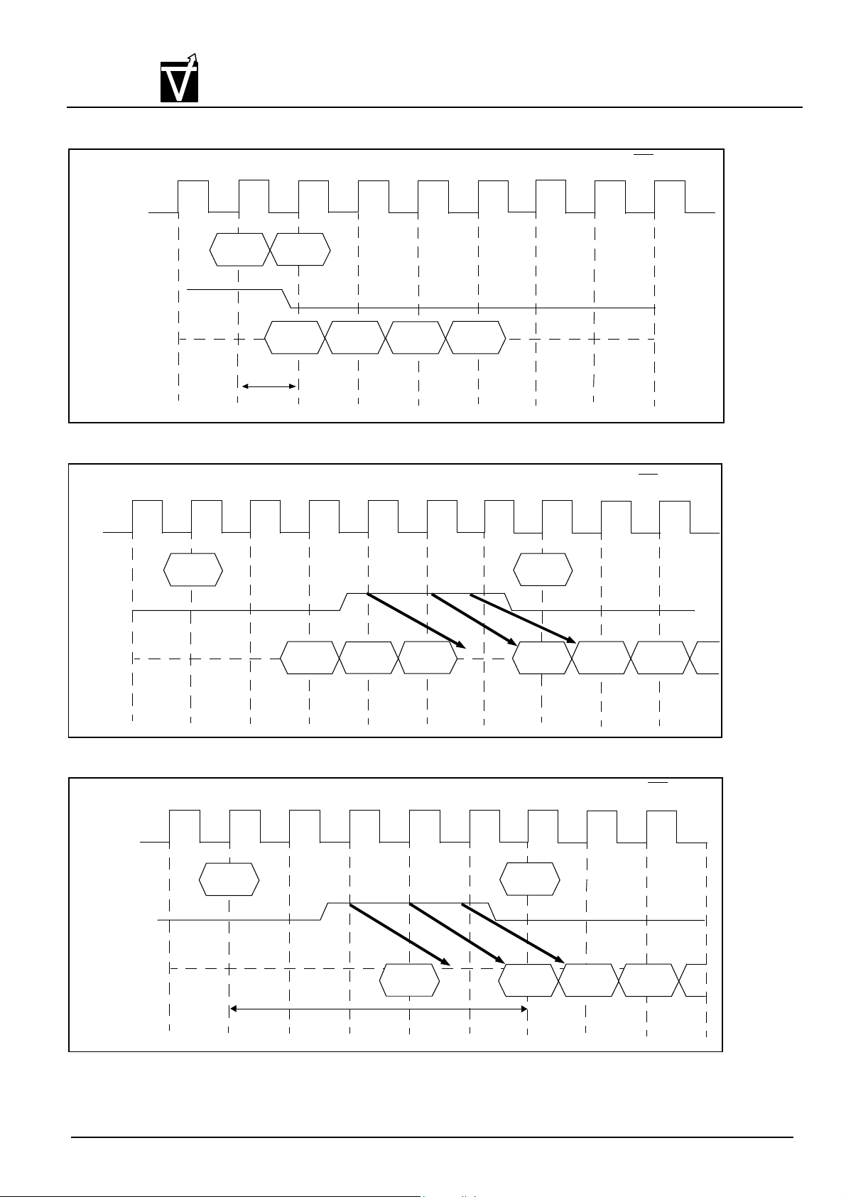
READ to WRITE Command Interval
CLK
CMOS Synchronous Dynamic RAM
T0 T1
T2
T3
T4 T5
T6
CAS latency = 2
T7
T8
command
DQM
DQ
CLK
Command
DQM
DQ
Hi-Z
T0 T1
Read
Read
1 cycle
Write
D0
T2
Q0
D1
T3
T4 T5
Q1
Q2
D3D2
Hi-Z is
necessary
Burst length = 8, CAS latency = 2
T6
T7
Write
D0
T8
D1
T9
D2
example: Burst length = 4, CAS latency = 3
CLK
Command
DQM
DQ
T0 T1
Read
The minimum command interval = (4+1) cycles
T2
T3
Q2
T4 T5
Hi-Z is
necessary
Write
D0
T6
D1
T7
D2
Document : 1G5-0099 Rev.1 Page 26
T8
Page 27
Preliminary VG3664321(4)1(2)BT
VIS
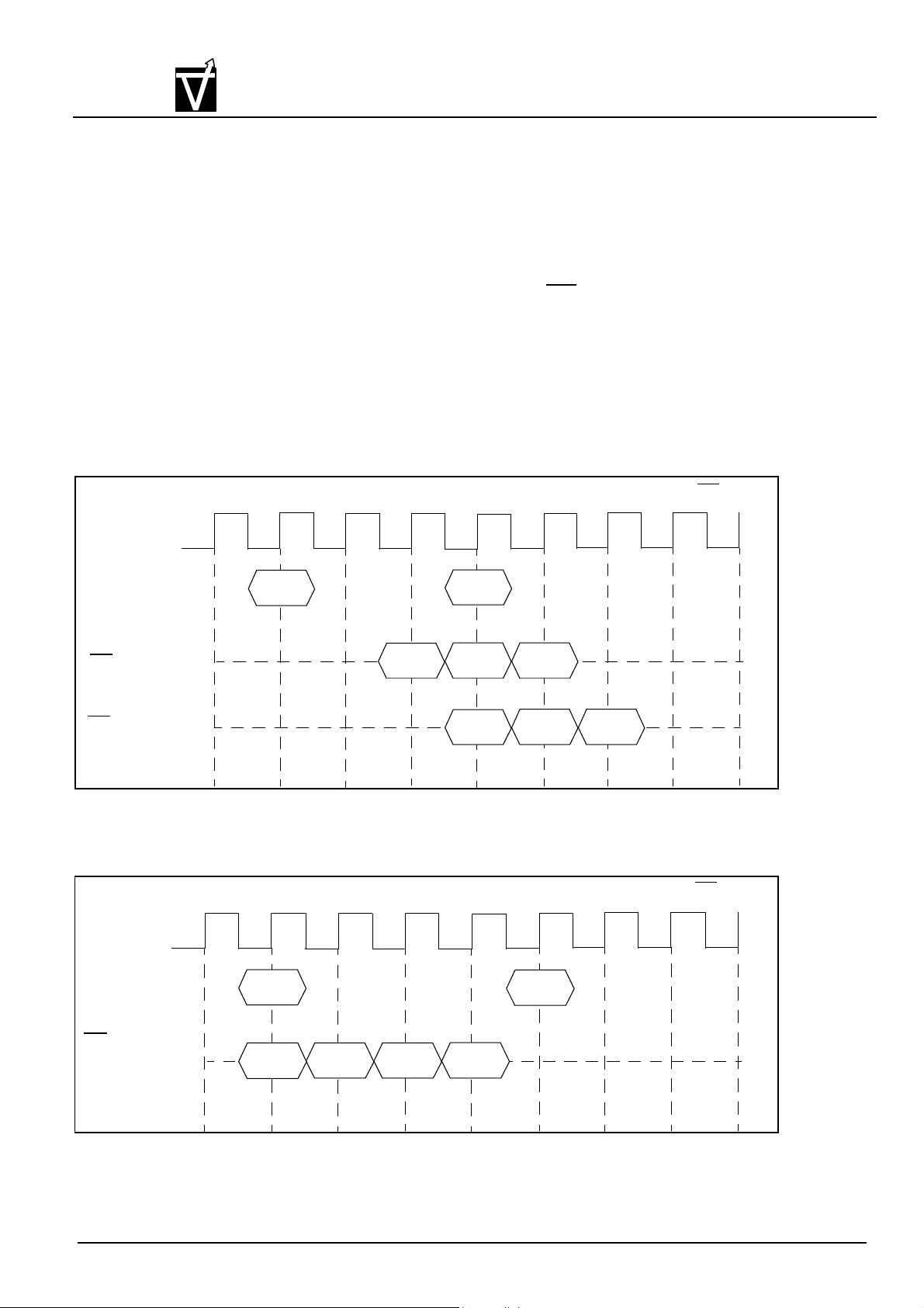
10. Burst Termination
There are two methods to terminate a burst operation other than using a read or a write
command. Ond is the burst stop command and the other is the precharge command.
10.1 Burst Stop Command
During a read burst, when the burst stop command is asserted, the burst read data are
terminated and the data bus goes to high - impedance after the CAS latency from the burst
stop command.
During a write burst, when the burst stop command is asserted, any data provided at
that cycle will not be written. The burst write is effectively terminated and no further data
can be written until a new write command is asserted.
Burst Termination
CMOS Synchronous Dynamic RAM
T0 T1
CLK
Command
CAS latency=2
DQ
CAS latency=3
DQ
Read
Remark BST : Burst stop command
T0 T1
T2
Burst length = X, CAS Intency=2,3
Q0
T3
T3
BST
Q1
Q0
T4 T5
Q2
Q1
T4 T5
T2
T6
Hi-Z
Q2
Burst length = X, CAS latency=2,3
T6
T7
Hi-Z
T7
CLK
Command
CAS latency=2,3
DQ
Write
Q0
Q0
Q1
Q2
BST
Hi-Z_
Remark BST : Burst stop command
Document : 1G5-0099 Rev.1 Page 27
Page 28
Preliminary VG3664321(4)1(2)BT
VIS
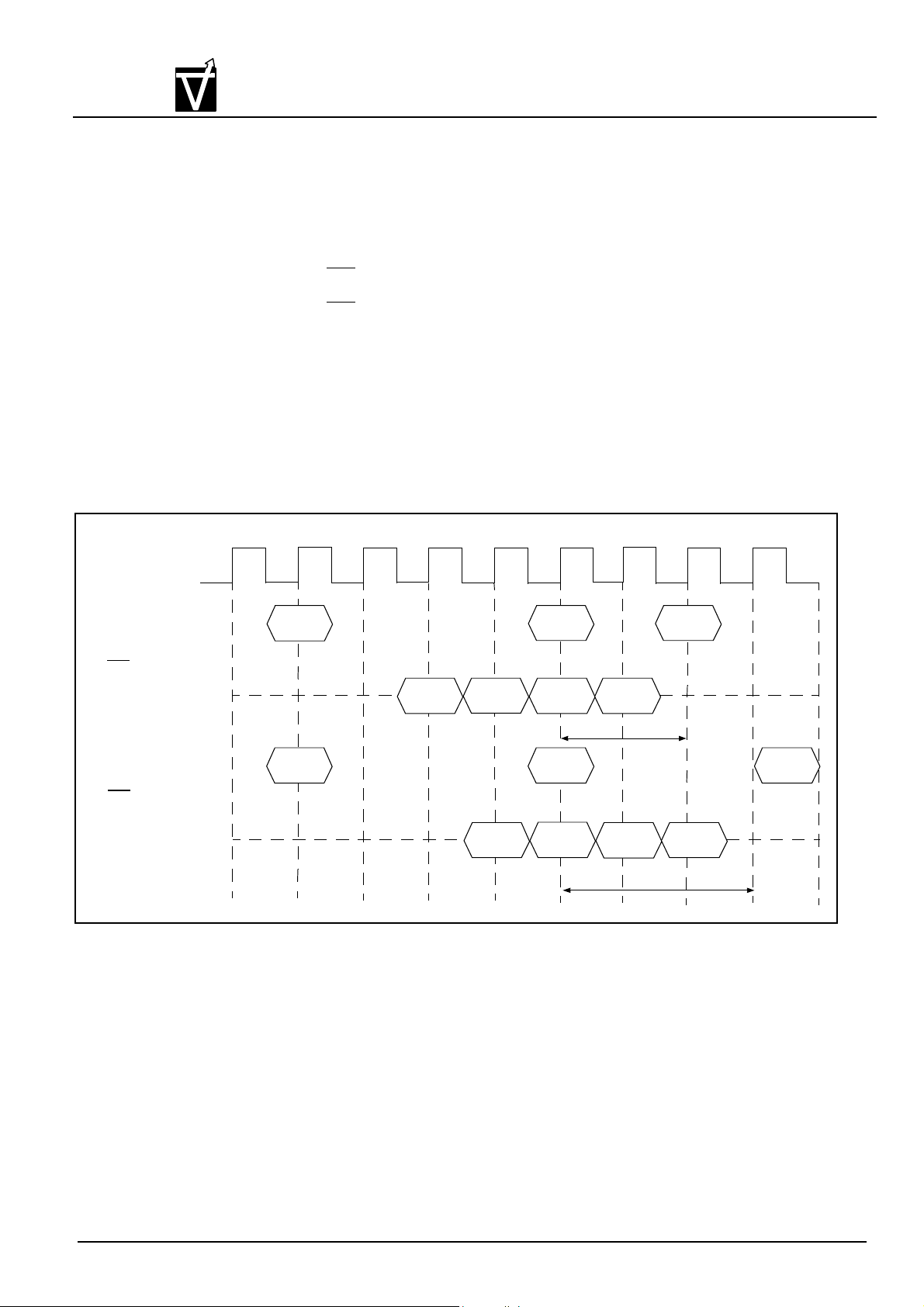
10.2 Precharge Termination
Precharge Termination in READ Cycle
CMOS Synchronous Dynamic RAM
10.2.1
During READ cycle, the burst read operation is terminated by a precharge command. When the precharge command is asserted, the burst read operation is terminated and precharge starts.
The same bank can be activated again after tRP from the precharge command.
When CAS latency is 2, the read data will remain valid until one clock after the
precharge command.
When CAS latency is 3, the read data will remain valid until two clocks after the
precharge command.
CLK
Command
CAS latency=2
DQ
command
CAS latency=3
DQ
T0 T1
Read
Read PRE ACT
T2
T3
Q0 Q3
T4 T5
PRE ACT
Q1
Q0 Q3
Q2
Q1
t
RP
Q2
T6
t
RP
T7
Hi-Z
Burst length = X
T8
Hi-Z
Document : 1G5-0099 Rev.1 Page 28
Page 29
VIS
Preliminary VG3664321(4)1(2)BT
CMOS Synchronous Dynamic RAM
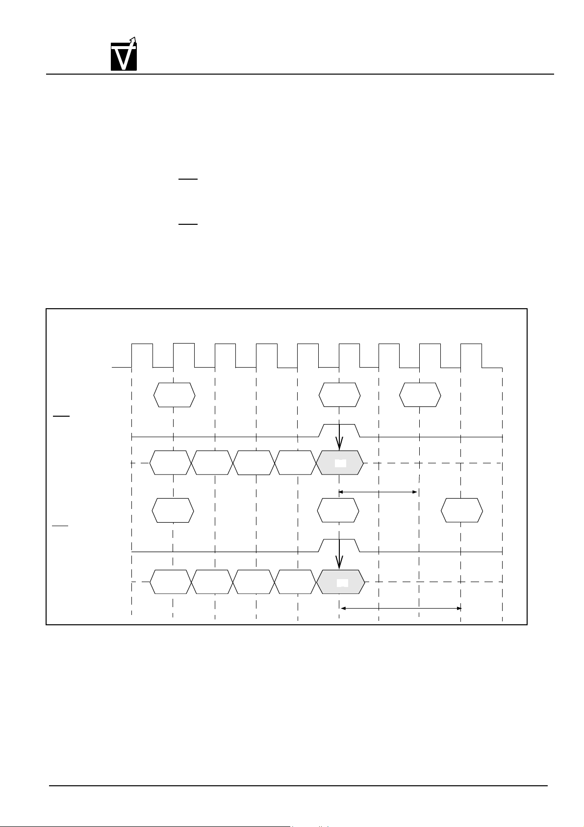
10.2.2 Precharge Termination in WRITE Cycle
During WRITE cycle, the burst write operation is terminated by a precharge
command. When the precharge command is asserted, the burst write operation is
terminated and precharge starts.
The same bank can be activated again after tRP from the precharge command.
The DQM must be high to mask invalid data in.
When CAS latency is 2, the write data written prior to the precharge command
will be correctly stored. However, invalid data may be written at the same clock as
the precharge command. To prevent this from happening, DQM must be high at the
same clock as the precharge command. This will mask the invalid data.
When CAS latency is 3, the write data written prior to the precharge command
will be correctly stored. However, invalid data may be written at the same clock as
the precharge command. To prevent this from happening, DQM must be high at the
same clock as the precharge command. This will mask the invalid data.
CLK
Command
CAS latency = 2
DQM
DQ
command
CAS latency = 3
DQM
DQ
T0 T1
Write
D0 D3
Write PRE ACT
D0 D3
T2
D1
D1
D2
D2
T3
T4 T5
PRE ACT
D4
t
RP
D4
T6
Hi - Z
t
RP
Hi - Z
Burst length = X
T7
T8
Document : 1G5-0099 Rev.1 Page 29
Page 30

VIS
Preliminary VG3664321(4)1(2)BT
CMOS Synchronous Dynamic RAM
Timing Diagram
Document : 1G5-0099 Rev.1 Page 30
Page 31
VIS
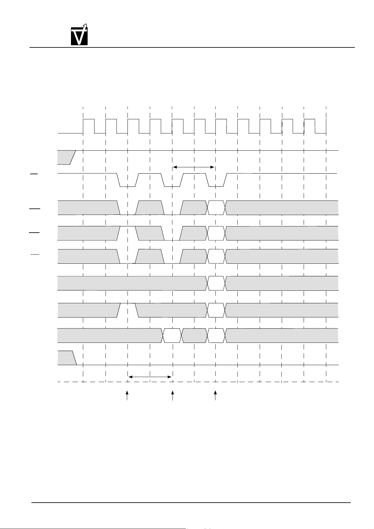
Mode Register Set
Preliminary VG3664321(4)1(2)BT
CMOS Synchronous Dynamic RAM
CLK
CKE
CS
RAS
CAS
WE
BS
T0
T1
T2
T3
T4
t
RSC
T5 T6
T7 T8
T9
T10
A10
ADD
DQM
DQ
Hi-Z
Precharge
Command
All Banks
Address Key
t
RP
Mode Register
Set Command
Command
Document : 1G5-0099 Rev.1 Page 31
Page 32
Preliminary VG3664321(4)1(2)BT
VIS
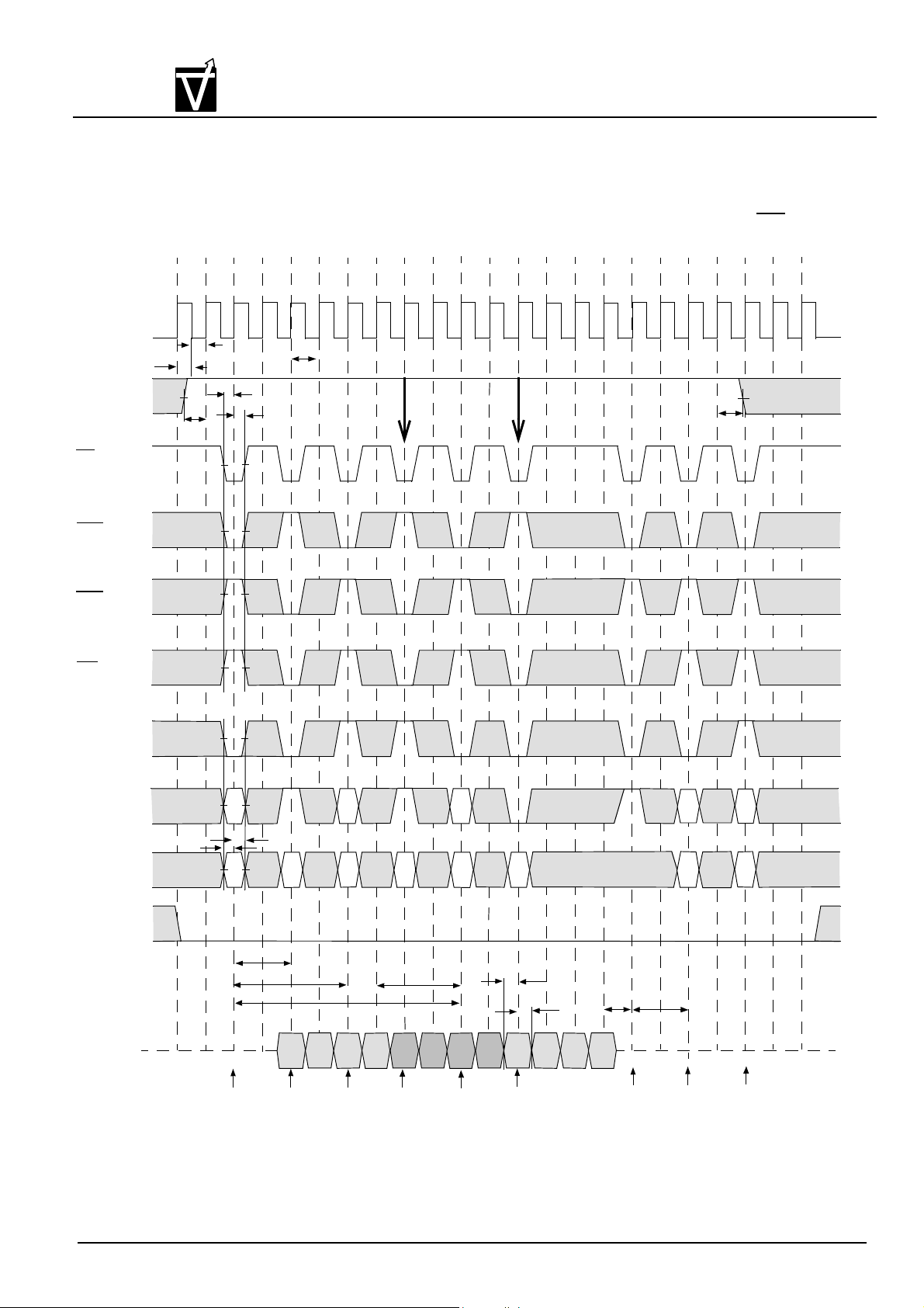
AC Parameters for Write Timing (1 of 2)
CMOS Synchronous Dynamic RAM
T0 T1 T2 T3 T4 T5 T6 T7 T8 T9 T10 T11 T12 T13 T14 T15 T16 T17 T18 T19 T20 T21 T22
Burst Length = 4, CAS Latency = 2
CLK
CKE
CS
RAS
CAS
WE
BS
t
CMS
t
CMH
t
CK2
Begin Auto Precharge
Bank A
Begin Auto Precharge
Bank B (Bank D)
t
CKH
t
CL
t
CH
t
CKS
A10
t
t
AS
AH
ADD
DQM
t
Activate
Bank A
RCD
t
RRD
QAa0
Write with
Auto Precharge
Command
Bank A
QAa1
t
RC
QAa2
Activate
Command
Bank B
(Bank D)
QAa3
QBa0 QBa1
Write with
Auto Precharge
Command
Bank B
(Bank D)
t
DAL
QBa2
Activate
Command
Bank A
QBa3 QAb0
Write with
Auto Precharge
Command
Bank A
t
DS
QAb1
t
t
QAb2
QAb3
DPL
Precharge
Command
Bank A
RP
Activate
Command
Bank A
Activate
Command
Bank B
(Bank D)
t
DH
DQ
Command
Document : 1G5-0099 Rev.1 Page 32
Page 33
Preliminary VG3664321(4)1(2)BT
VIS
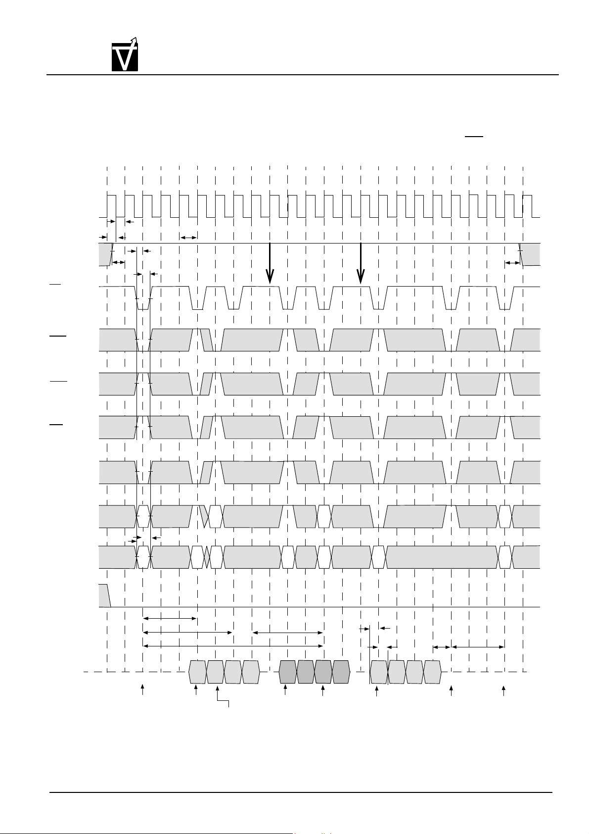
AC Parameters for Write Timing (2 of 2)
CMOS Synchronous Dynamic RAM
T0 T1 T2 T3 T4 T5 T6 T7 T8 T9 T10 T11 T12 T13 T14 T15 T16 T17 T18 T19 T20 T21 T22 T23
Burst Length = 4, CAS Latency = 3
CLK
CKE
CS
RAS
CAS
WE
BS
t
CL
t
CH
t
CKS
t
CMS
t
CMH
t
CK3
Begin Auto Precharge
Bank A
Begin Auto Precharge
Bank B (Bank D)
t
CKH
A10
t
t
AS
AH
ADD
DQM
t
RCD
DQ
Activate
Command
Bank A
t
RRD
QAa0
Write with
Auto Precharge
Command
Bank A
QAa1
t
RC
QAa2
Activate
Command
Bank B
(Bank D)
QAa3 QBa0
t
DAL
Write with
Auto Precharge
Command
Bank B
(Bank D)
QBa1 QBa2
Activate
Command
Bank A
QBa3
t
DS
t
DH
QAb0
QAb1 QAb2
Write without
Auto Precharge
Command
Bank A
QAb3
t
DPL
Precharge
Command
Bank A
t
RP
Activate
Command
Bank A
Document : 1G5-0099 Rev.1 Page 33
Page 34
Preliminary VG3664321(4)1(2)BT
VIS
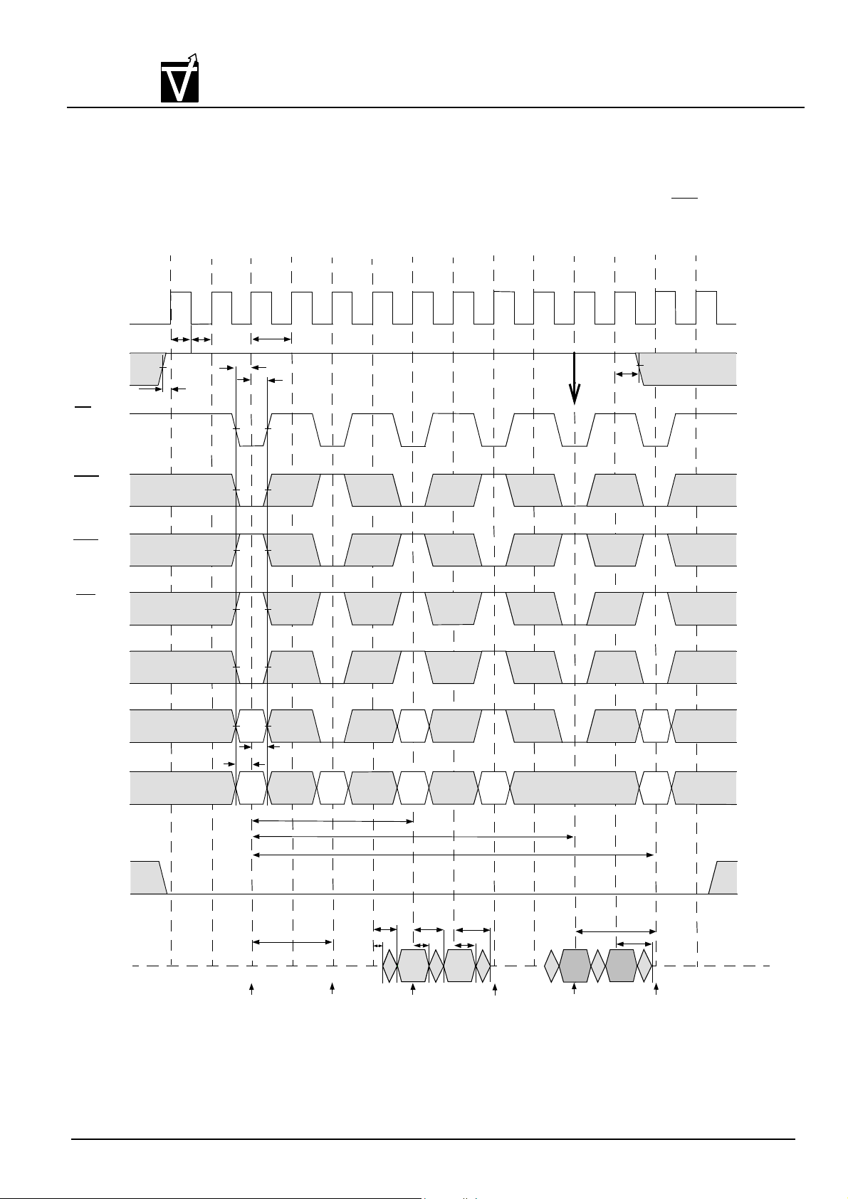
AC Parameters for Read Timing (1 of 2)
CMOS Synchronous Dynamic RAM
T0 T1 T2 T3 T4 T5 T6 T7 T8 T9 T10 T11 T12 T13
Burst Length = 2, CAS Latency = 2
CLK
CKE
CS
RAS
CAS
WE
BS
A10
ADD
tCHt
t
CKS
CL
t
AS
t
AH
t
CK2
t
CMS
t
CMH
Begin Auto
Precharge
Bank B (Bank D)
t
CKH
t
RRD
t
RAS
t
RC
DQM
t
DQ
Hi-Z
Activate
Command
Bank A
t
RCD
Read
Command
Bank A
AC2
t
LZ
t
AC2
t
OH
QAa0
Activate
Command
Bank B
t
HZ
t
OH
QAa1
Read with
Auto Precharge
Bank B (Bank D)
t
RP
QBa0
Precharge
Command
Bank B (Bank D)
QBa1
t
HZ
Activate
Command
Bank A
Document : 1G5-0099 Rev.1 Page 34
Page 35
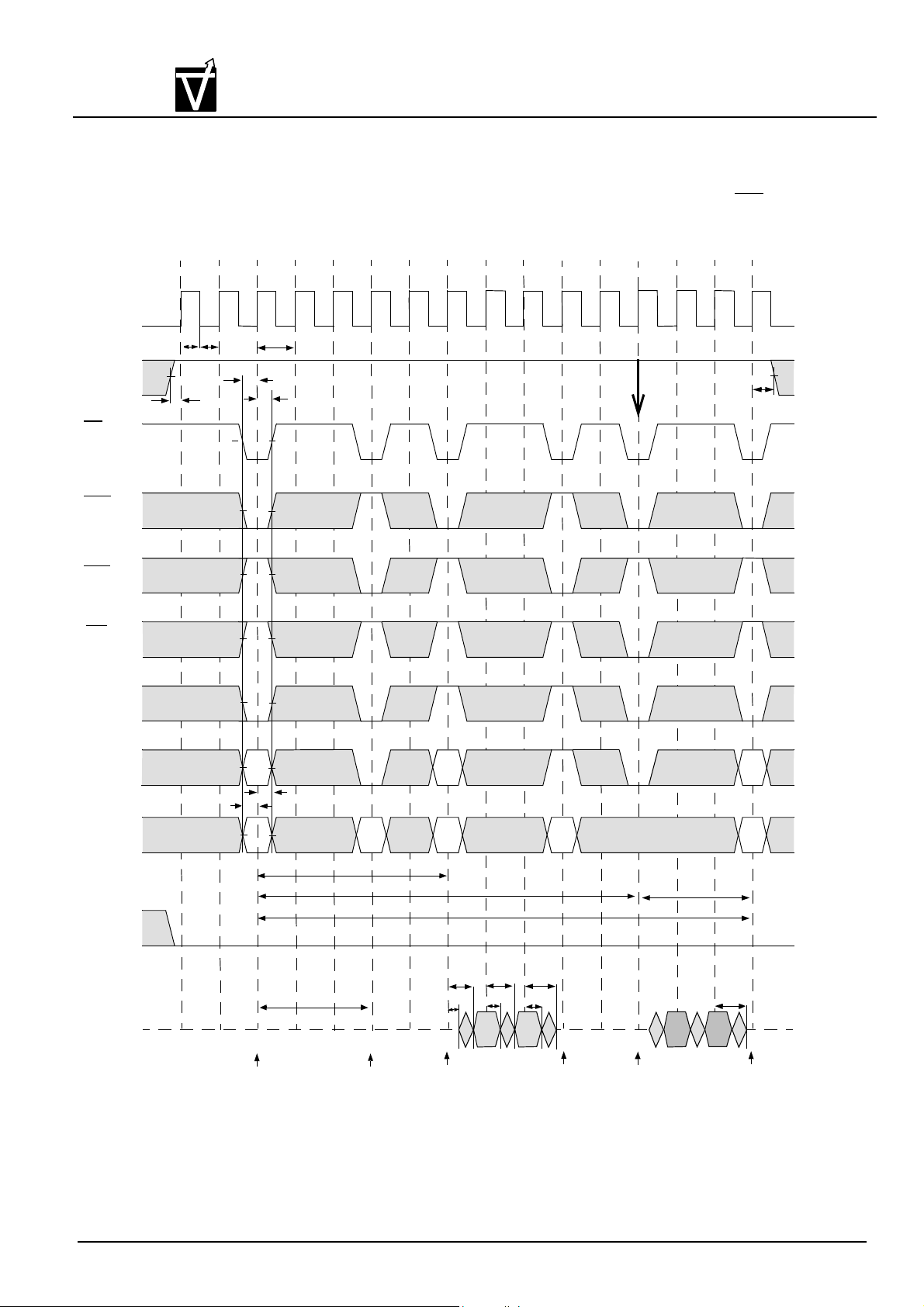
Preliminary VG3664321(4)1(2)BT
VIS
AC Parameters for Read Timing (2 of 2)
CMOS Synchronous Dynamic RAM
T0 T1 T2 T3 T4 T5 T6 T7 T8 T9 T10 T11 T12 T13 T14 T15
Burst Length = 2, CAS Latency = 3
CLK
CKE
CS
RAS
CAS
WE
BS
A10
ADD
t
CH
t
CKS
t
CL
t
CK3
t
CMS
t
CMH
t
AH
t
AS
Begin Auto
Precharge
Bank B (Bank D)
t
CKH
t
RRD
t
RAS
t
RC
t
RP
DQM
t
AC3
t
OH
Read with
Auto Precharge
Command
Bank B (Bank D)
t
t
HZ
OH
Precharge
Command
Bank A
QBa0
QBa1
t
HZ
DQ
Hi-Z
Activate
Command
Bank A
t
RCD
Read
Command
Bank A
t
AC3
t
LZ
Activate
Command
Bank B
(Bank D)
QAa0 QAa1
Document : 1G5-0099 Rev.1 Page 35
Activate
Command
Bank A
Page 36
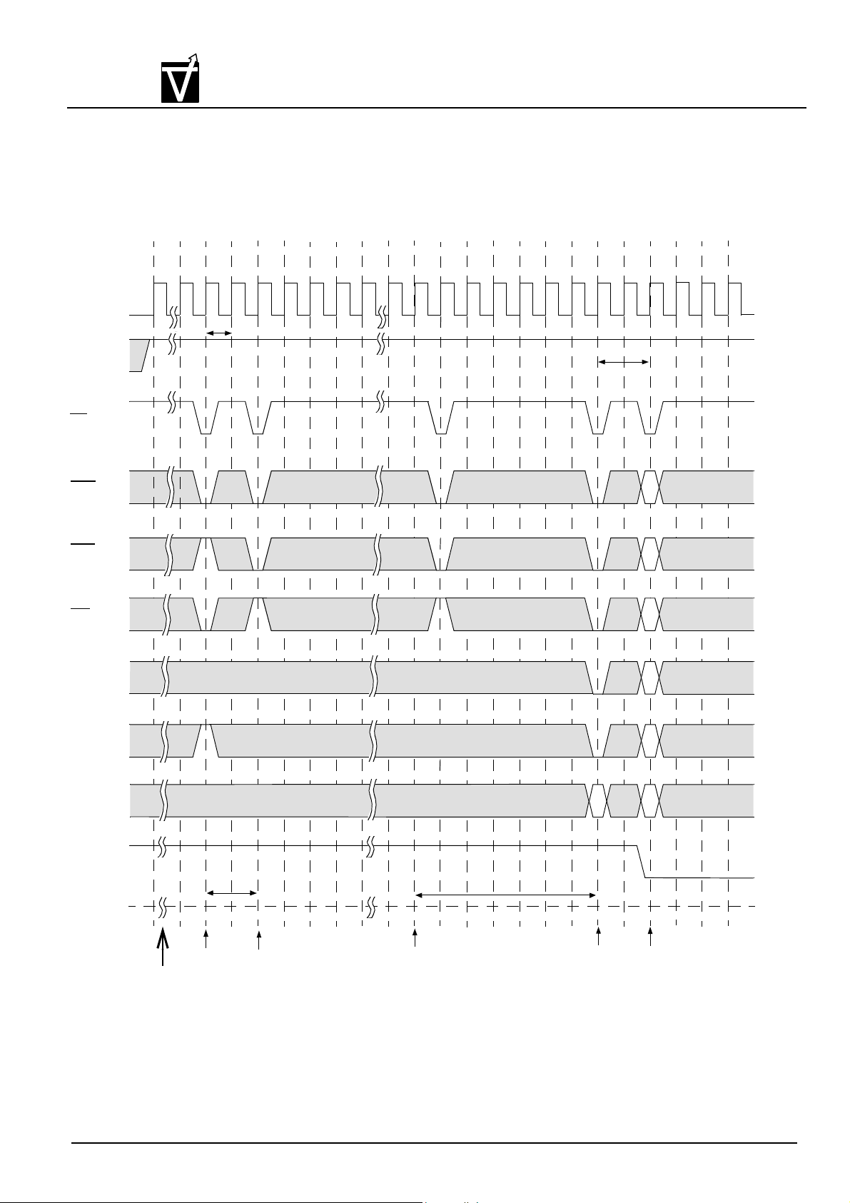
Preliminary VG3664321(4)1(2)BT
VIS
Power on Sequence and Auto Refresh (CBR)
T0 T1 T2 T3 T4 T5 T6 T7 T8 T9 T10 T11 T12 T13 T14 T15 T16 T17 T18 T19 T20 T21 T22
CLK
CMOS Synchronous Dynamic RAM
CKE
CS
RAS
CAS
WE
BS
A10
High level
is required
Minimum of 2 Refresh Cycles are required
t
RSC
Address Key
ADD
DQM
High Level is Necessary
t
RP
t
RC
DQ
Mode
Register
Set Command
Command
Inputs
must
be stable
for 100us
Precharge
Command
All Banks
1st Auto
Refresh
Command
2nd Auto
Refresh
Command
Document : 1G5-0099 Rev.1 Page 36
Page 37
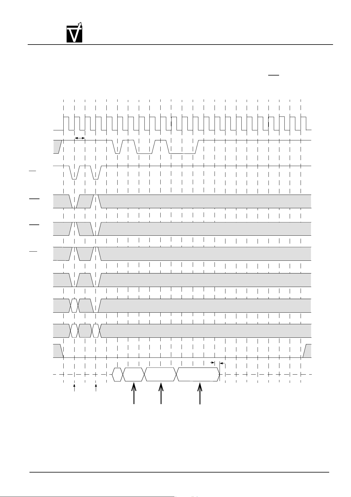
Preliminary VG3664321(4)1(2)BT
VIS
Clock Suspension During Burst Read (Using CKE) (1 of 2)
T0 T1 T2 T3 T4 T5 T6 T7 T8 T9 T10 T11 T12 T13 T14 T15 T16 T17 T18 T19 T20 T21 T22
CMOS Synchronous Dynamic RAM
Burst Length = 4, CAS Latency = 2
CLK
CKE
CS
RAS
CAS
WE
BS
t
CK2
Hi-Z
RAa
RAa
Activate
Command
Bank A
CAa
Read
Command
Bank A
QAa0 QAa1 QAa2 QAa3
Clock
Suspended
1 Cycle
Clock
Suspended
2 Cycle
Clock
Suspended
3 Cycle
t
HZ
A10
ADD
DQM
DQ
Document : 1G5-0099 Rev.1 Page 37
Page 38
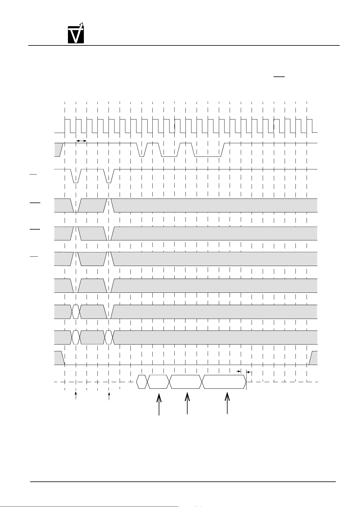
Preliminary VG3664321(4)1(2)BT
VIS
Clock Suspension During Burst Read (Using CKE) (2 of 2)
T0 T1 T2 T3 T4 T5 T6 T7 T8 T9 T10 T11 T12 T13 T14 T15 T16 T17 T18 T19 T20 T21 T22
CMOS Synchronous Dynamic RAM
Burst Length = 4, CAS Latency = 3
CLK
CKE
CS
RAS
CAS
WE
BS
t
CK3
Hi-Z
RAa
RAa
Activate
Command
Bank A
CAa
Read
Command
Bank A
QAa0
QAa1
Clock
Suspended
1 Cycle
QAa2 QAa3
Clock
Suspended
2 Cycle
Suspended
t
Clock
3 Cycle
HZ
A10
ADD
DQM
DQ
Document : 1G5-0099 Rev.1 Page 38
Page 39
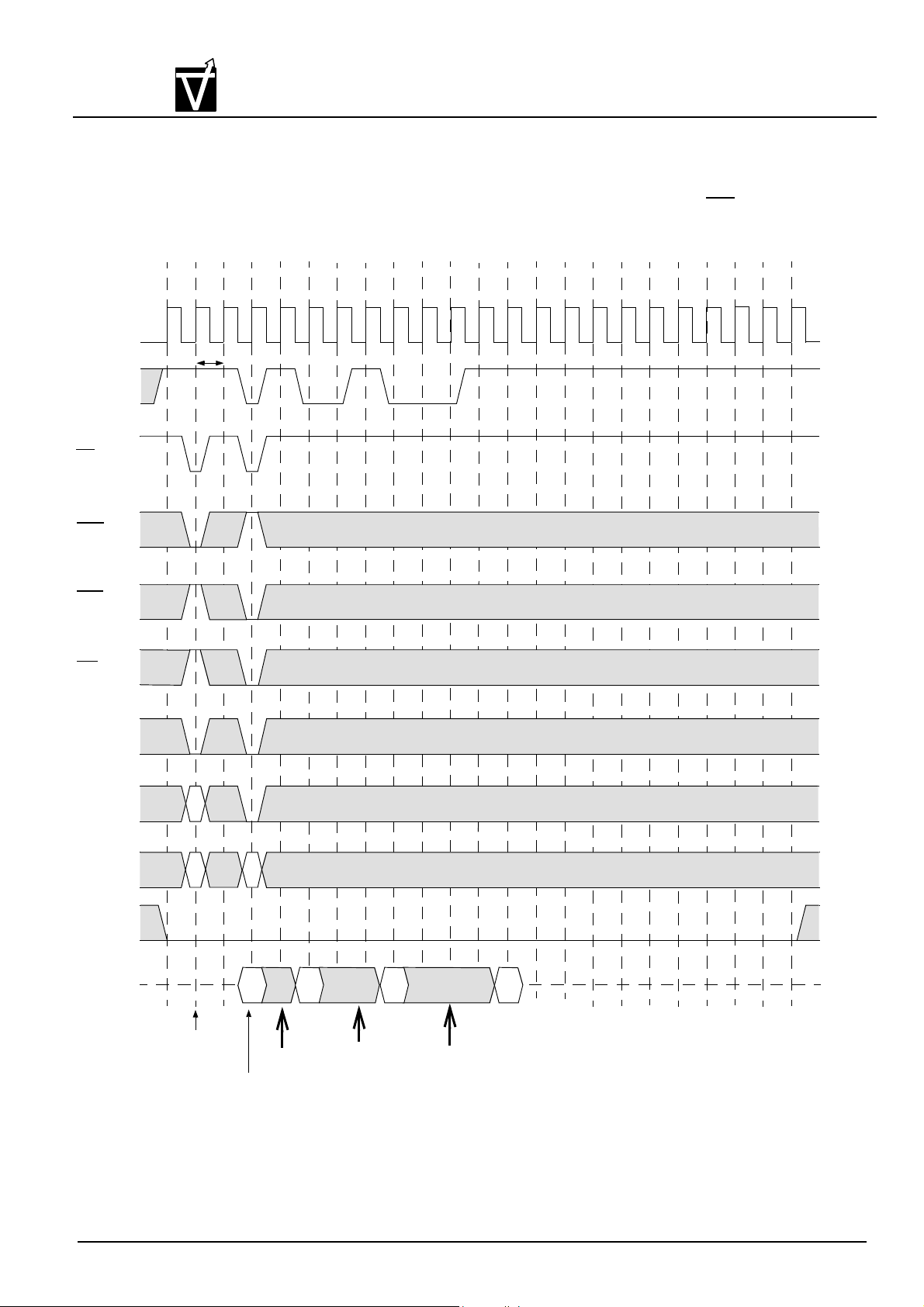
Preliminary VG3664321(4)1(2)BT
VIS
Clock Suspension During burst Write (Using CKE) (1 of 2)
T0 T1 T2 T3 T4 T5 T6 T7 T8 T9 T10 T11 T12 T13 T14 T15 T16 T17 T18 T19 T20 T21 T22
CMOS Synchronous Dynamic RAM
Burst Length = 4, CAS Latency = 2
CLK
CKE
CS
RAS
CAS
WE
BS
t
CK2
A10
ADD
RAa
RAa
CAa
DQM
DQ
Hi-Z
Activate
Command
Bank A
DAa0 DAa1 DAa2 DAa3
Clock
Suspended
2 Cycle
Clock
Suspended
3 Cycle
Write
Command
Bank A
Clock
Suspended
1 Cycle
Document : 1G5-0099 Rev.1 Page 39
Page 40
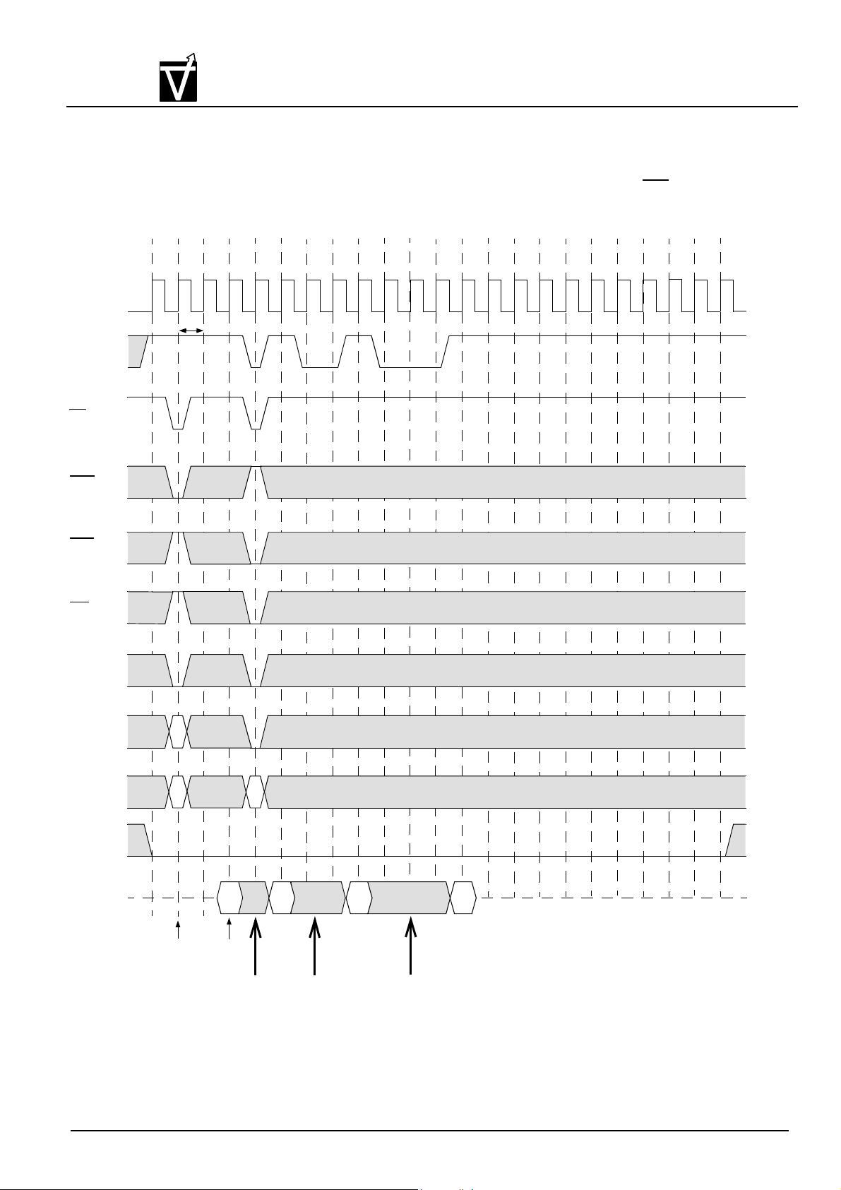
Preliminary VG3664321(4)1(2)BT
VIS
Clock suspension during Burst write (Using CKE) (2 of 2)
T0 T1 T2 T3 T4 T5 T6 T7 T8 T9 T10 T11 T12 T13 T14 T15 T16 T17 T18 T19 T20 T21 T22
CMOS Synchronous Dynamic RAM
Burst Length = 4, CAS Latency = 3
CLK
CKE
CS
RAS
CAS
WE
BS
t
CK3
Hi-Z
RAa
RAa
Activate
Command
Bank A
CAa
DAa0 DAa1 DAa2 DAa3
Write
Command
Bank A
Clock
Suspended
1 Cycle
Clock
Suspended
1 Cycle
Clock
Suspended
1 Cycle
t
A10
ADD
DQM
DQ
Document : 1G5-0099 Rev.1 Page 40
Page 41
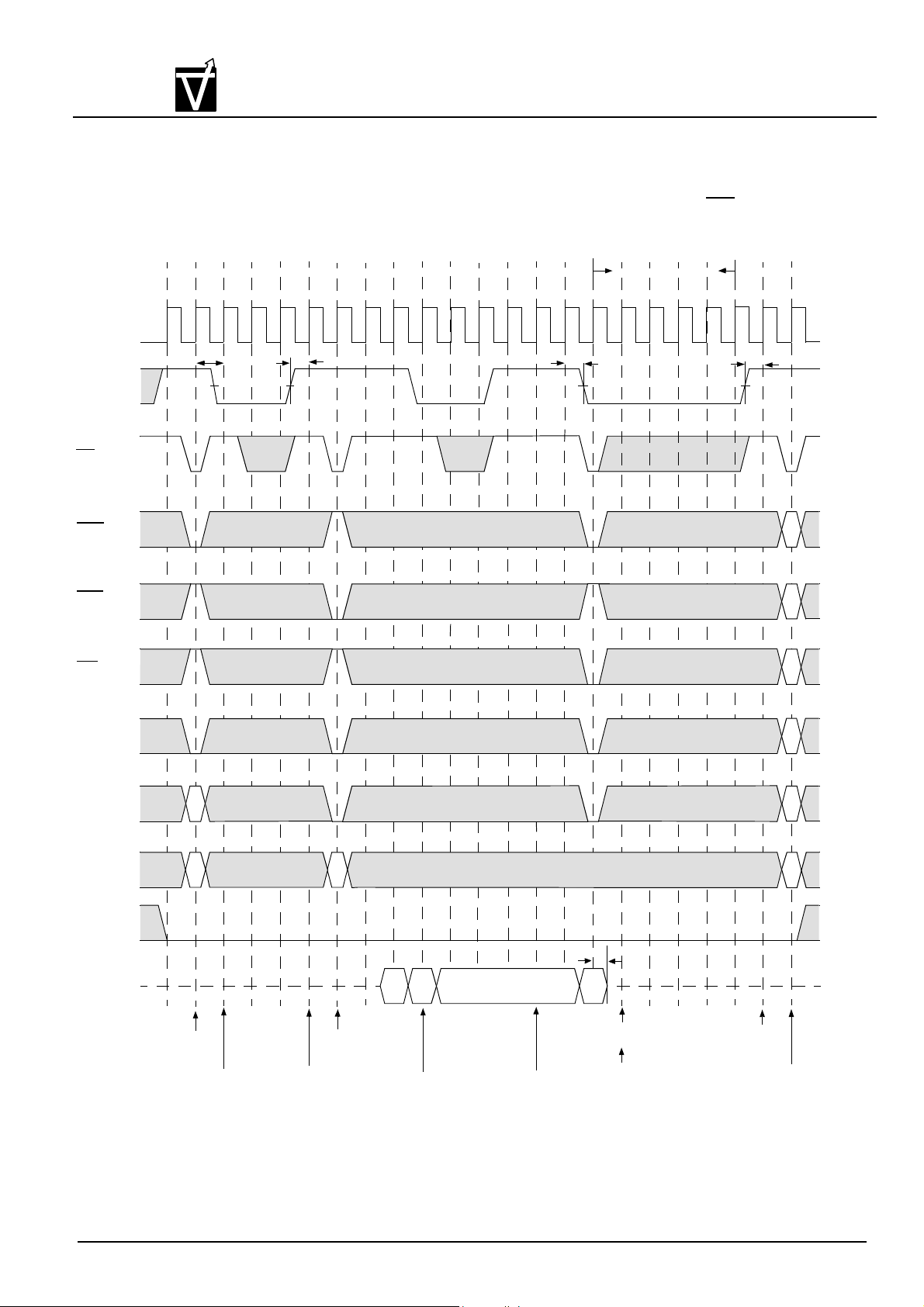
Preliminary VG3664321(4)1(2)BT
VIS
Power Down Mode and Clock Mask
CMOS Synchronous Dynamic RAM
Burst Length = 4, CAS Latency = 2
CLK
CKE
CS
RAS
CAS
WE
T0 T1 T2 T3 T4 T5 T6 T7 T8 T9 T10 T11 T12 T13 T14 T15 T16 T17 T18 T19 T20 T21 T22
CLK can be Stopped *
t
CK2
t
CKS
t
CKH
VALID
t
CKS
BS
A10
ADD
DQM
DQ
Hi-Z
RAa
RAa
RAa
Activate
Command
Bank A
Power Down
Mode Entry
ACTIVE
STANDBY
CAa
Read
Command
Bank A
Power Down
Mode Exit
QAa0
QAa1
Clock Mask
Start
QAa2
Clock Mask
End
t
HZ
QAa3
Precharge
Command
Power Down
Mode Entry
Precharge
Standby
Power
Down
Mode
Exit
Command
Document : 1G5-0099 Rev.1 Page 41
Page 42
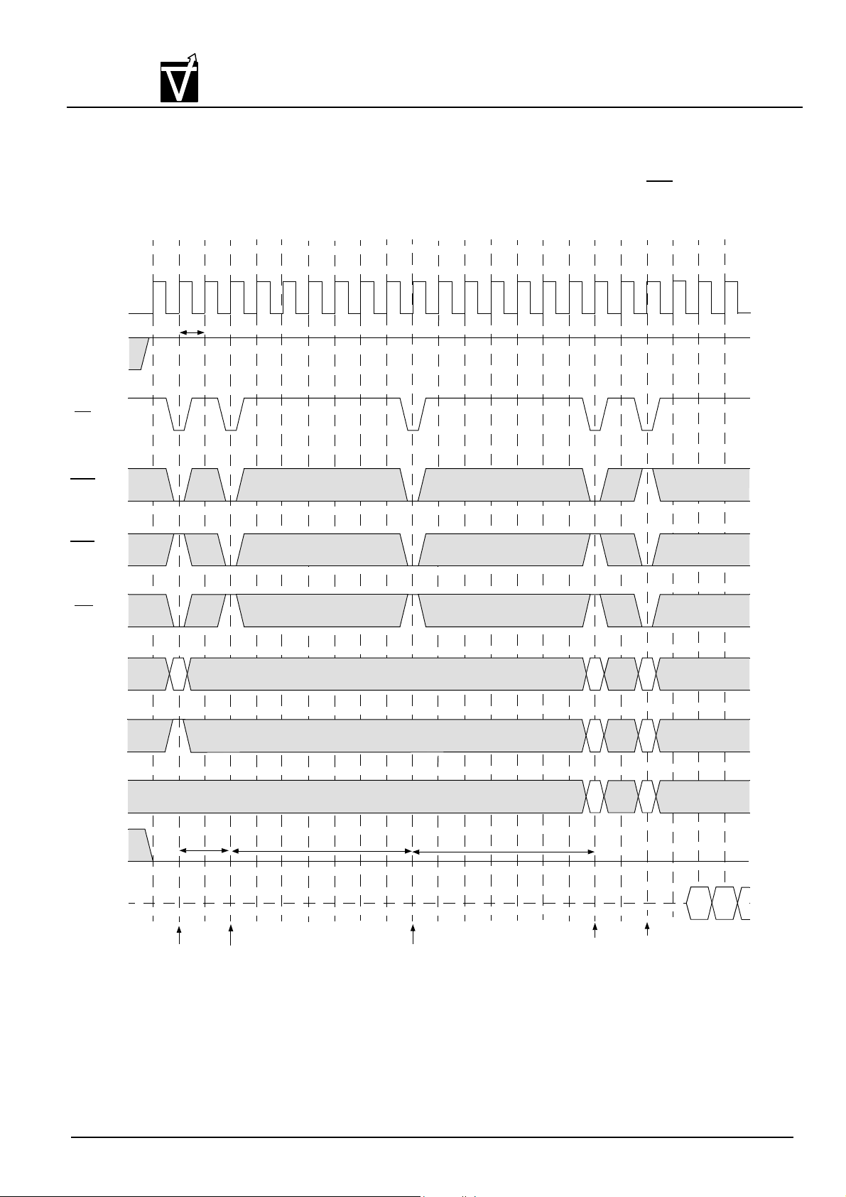
VIS
Auto Refresh (CBR)
T0 T1 T2 T3 T4 T5 T6 T7 T8 T9 T10 T11 T12 T13 T14 T15 T16 T17 T18 T19 T20 T21 T22
Preliminary VG3664321(4)1(2)BT
CMOS Synchronous Dynamic RAM
Burst Length = 4, CAS Latency = 2
CLK
CKE
CS
RAS
CAS
WE
BS
t
CK2
A10
ADD
t
t
RP
RC
t
RC
RAa
RAa
CAa
DQM
DQ
Hi-Z
Precharge
Command
All Banks
CBR Refresh
Command
CBR Refresh
Command
Activate
Command
Read
Command
Q0 Q1
Document : 1G5-0099 Rev.1 Page 42
Page 43
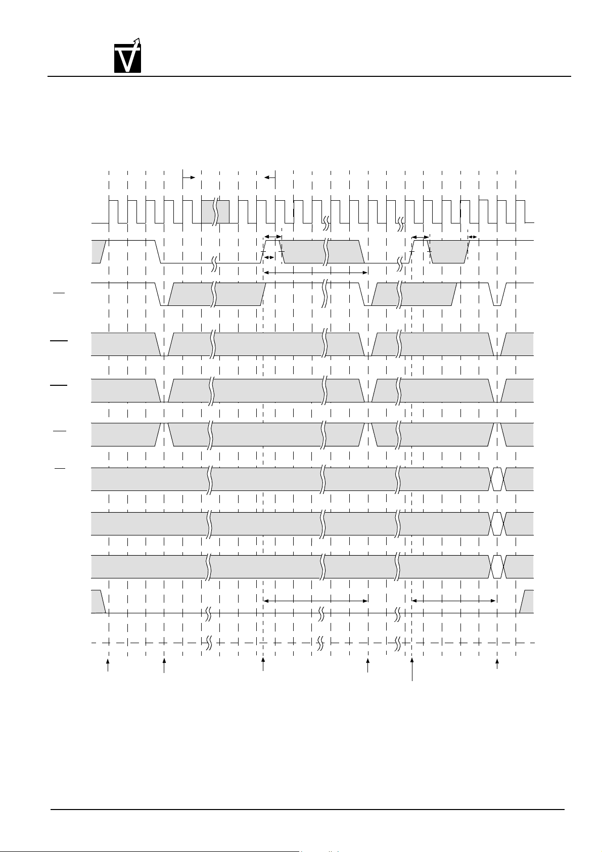
Preliminary VG3664321(4)1(2)BT
VIS
Self Refresh (Entry and Exit)
CMOS Synchronous Dynamic RAM
CLK
CKE
CS
RAS
CAS
WE
T0 T1 T2 T3 T4 T5 T6 T7 T8 T9 T10 T11 T12 T13 T14 T15 T16 T17 T18 T19 T20 T21 T22
CLK can be Stopped *
t
CKS
t
SRX
t
SRX
t
CKS
BS
A10
ADD
DQM
DQ
Hi-Z
All Banks
must be idle
Self refresh
Entry
Self Refresh
Exit
t
RC
Self Refresh
Exit
Self Refresh
Exit
t
RC
Activate
Command
Document : 1G5-0099 Rev.1 Page 43
Page 44
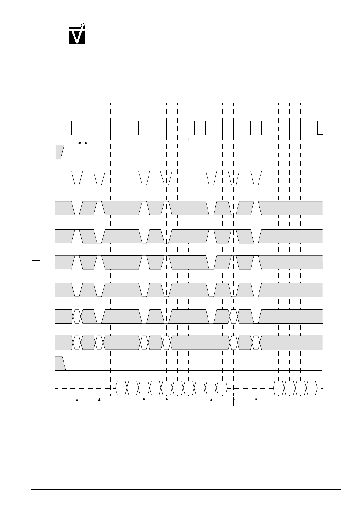
Preliminary VG3664321(4)1(2)BT
VIS
Random Column Read (Page Within same Bank)(1 of 2)
T0 T1 T2 T3 T4 T5 T6 T7 T8 T9 T10 T11 T12 T13 T14 T15 T16 T17 T18 T19 T20 T21 T22
CMOS Synchronous Dynamic RAM
Burst Length = 4, CAS Latency = 2
CLK
CKE
CS
RAS
CAS
WE
BS
t
CK2
A10
ADD
RAa
RAa
CAa
CAb CAc
RAa
RAd
RAd
CAd
DQM
DQ
Hi-Z
Precharge
Command
Bank A
Read
Command
Bank A
QAa0 QAa1
QAa2 QAa3 QAb0
Read
Command
Bank A
QAb1
Read
Command
Bank A
QAc0 QAc1 QAc2
Precharge
Command
Bank A
QAc3
Activate
Command
Bank A
Read
Command
Bank A
QAd0
QAd1
QAd2
Document : 1G5-0099 Rev.1 Page 44
QAd3
Page 45
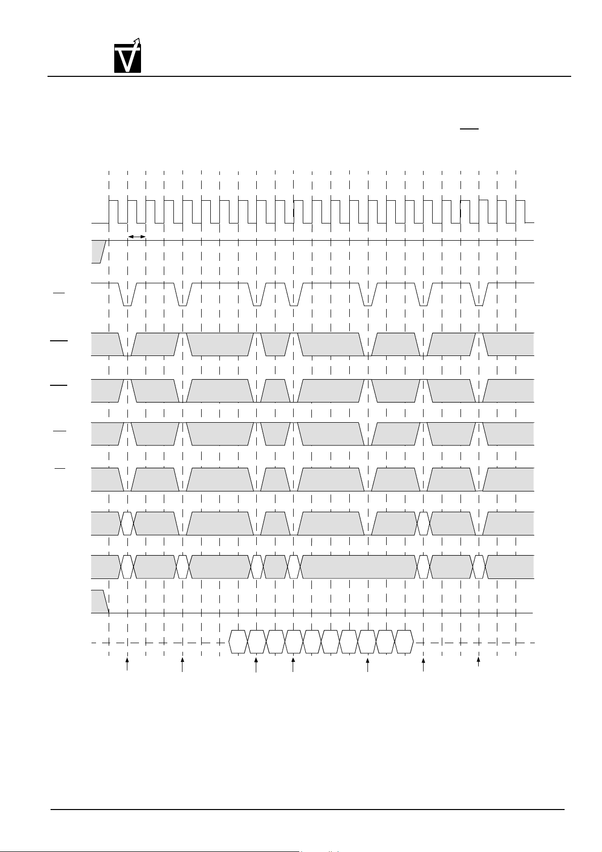
Preliminary VG3664321(4)1(2)BT
VIS
Random Column Read (Page Within same Bank)(2 of 2)
T0 T1 T2 T3 T4 T5 T6 T7 T8 T9 T10 T11 T12 T13 T14 T15 T16 T17 T18 T19 T20 T21 T22
CMOS Synchronous Dynamic RAM
Burst Length = 4, CAS Latency = 3
CLK
CKE
CS
RAS
CAS
WE
BS
t
CK3
A10
ADD
RAa
RAa
CAa
CAb CAc RAd
RAd
CAd
DQM
DQ
Hi-Z
Activate
Command
Bank A
Read
Command
Bank A
QAa0 QAa1 QAa2
Read
Command
Bank A
QAa3
Read
Command
Bank A
QAb0 QAb1 QAc0
QAc1
Precharge
Command
Bank A
QAc2 QAc3
Activate
Command
Bank A
Read
Command
Bank A
Document : 1G5-0099 Rev.1 Page 45
Page 46
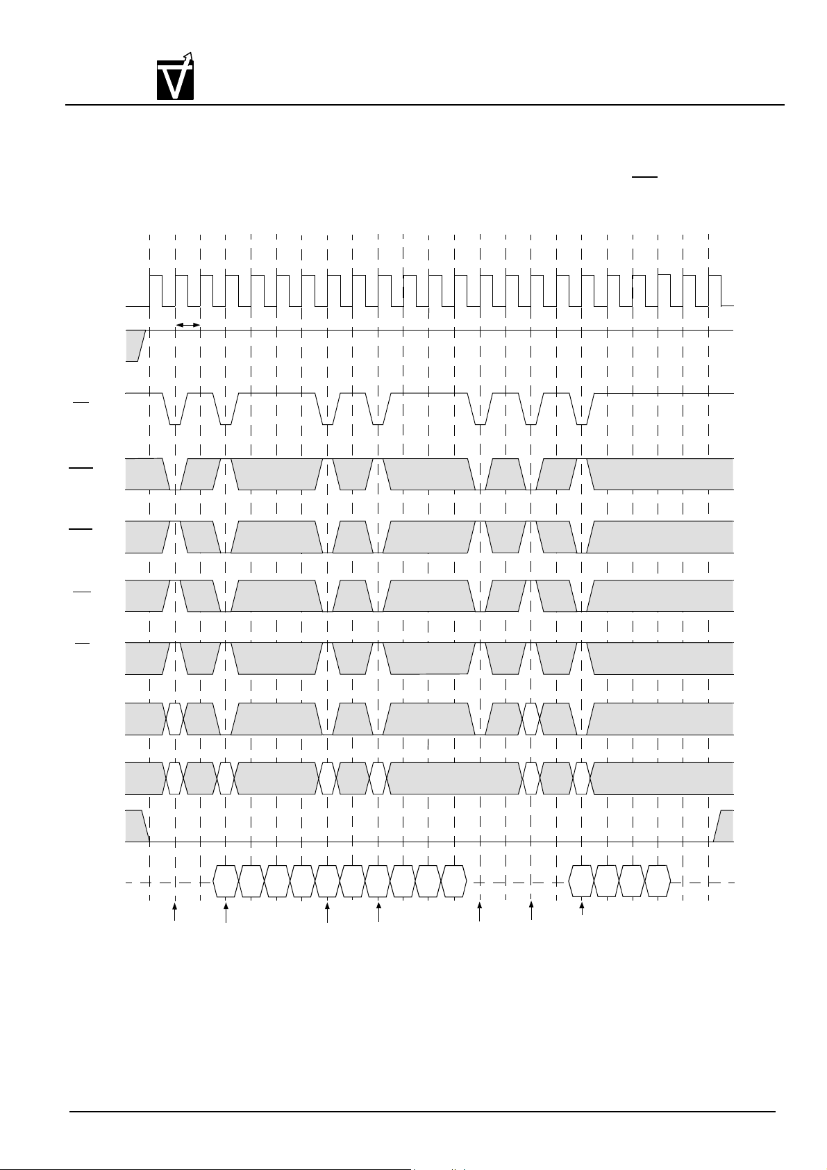
Preliminary VG3664321(4)1(2)BT
VIS
Random Column Write (Page Within same Bank) (1 of 2)
T0 T1 T2 T3 T4 T5 T6 T7 T8 T9 T10 T11 T12 T13 T14 T15 T16 T17 T18 T19 T20 T21 T22
CMOS Synchronous Dynamic RAM
Burst Length = 4, CAS Latency = 2
CLK
CKE
CS
RAS
CAS
WE
BS
t
CK2
A10
ADD
Ra
Ra
Ca
Cb Cc Rd
Rd
Cd
DQM
DQ
Hi-Z
Activate
Command
Bank B
(Bank D)
Da0
Write
Command
Bank B
(Bank D)
Da1 Da2
Db0 Db1 Dc0
Da3
Write
Command
Bank B
(Bank D)
Write
Command
Bank B
(Bank D)
Dc1
Dc2 Dc3
Precharge
Command
Bank B
(Bank D)
Activate
Command
Bank B
(Bank D)
Dd0
Dd1
Write
Command
Bank B
(Bank D)
Dd2 Dd3
Document : 1G5-0099 Rev.1 Page 46
Page 47
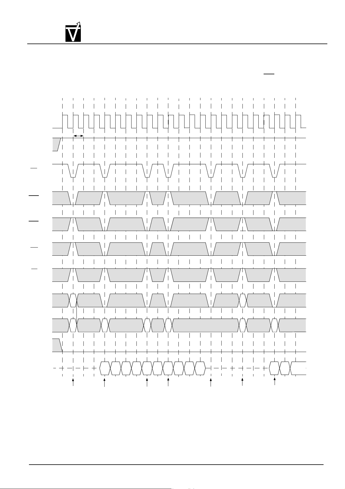
Preliminary VG3664321(4)1(2)BT
VIS
Random Column Write (Page Within same Bank) (2 of 2)
T0 T1 T2 T3 T4 T5 T6 T7 T8 T9 T10 T11 T12 T13 T14 T15 T16 T17 T18 T19 T20 T21 T22
CMOS Synchronous Dynamic RAM
Burst Length = 4, CAS Latency = 3
CLK
CKE
CS
RAS
CAS
WE
BS
t
CK3
A10
ADD
Ra
Ra
Ca
Cb
Cc Rd
Rd
Cd
DQM
DQ
Hi-Z
Activate
Command
Bank B
(Bank D)
Write
Command
Bank B
(Bank D)
Da1 Da2
Db0 Db1 Dc0
Da3
Write
Command
Bank B
(Bank D)
Write
Command
Bank B
(Bank D)
Dc1
Dc2
Dc3
Precharge
Command
Bank B
(Bank D)
Activate
Command
Bank B
(Bank D)
Dd0
Dd1Da0
Write
Command
Bank B
(Bank D)
Document : 1G5-0099 Rev.1 Page 47
Page 48
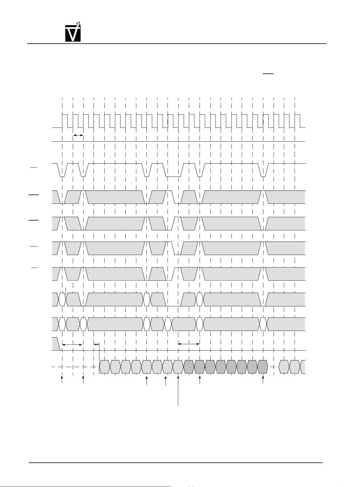
Preliminary VG3664321(4)1(2)BT
VIS
Random Row Read (Interleaving Banks) (1 of 2)
T0 T1 T2 T3 T4 T5 T6 T7 T8 T9 T10 T11 T12 T13 T14 T15 T16 T17 T18 T19 T20 T21 T22
CMOS Synchronous Dynamic RAM
Burst Length = 8, CAS Latency = 2
CLK
CKE
CS
RAS
CAS
WE
BS
High
t
CK2
A10
ADD
t
RCD
t
AC2
t
RP
DQM
DQ
Hi-Z
Activate
Command
Bank B
(Bank D)
Read
Command
Bank B
(Bank D)
QBa1 QBa2
QBa4
QBa3
Activate
Command
Bank A
QBa5 QBa6 QBa7
Read
Command
Bank A
Precharge
Command
Bank B
(Bank D)
QAa0
Active
Command
Bank B
(Bank D)
QAa1
QAa2
QAa3 QAa4
QAa5
QAa6 QAa7
Read
Command
Bank B
(Bank D)
QBb0QBa0
Document : 1G5-0099 Rev.1 Page 48
QBb1
Page 49
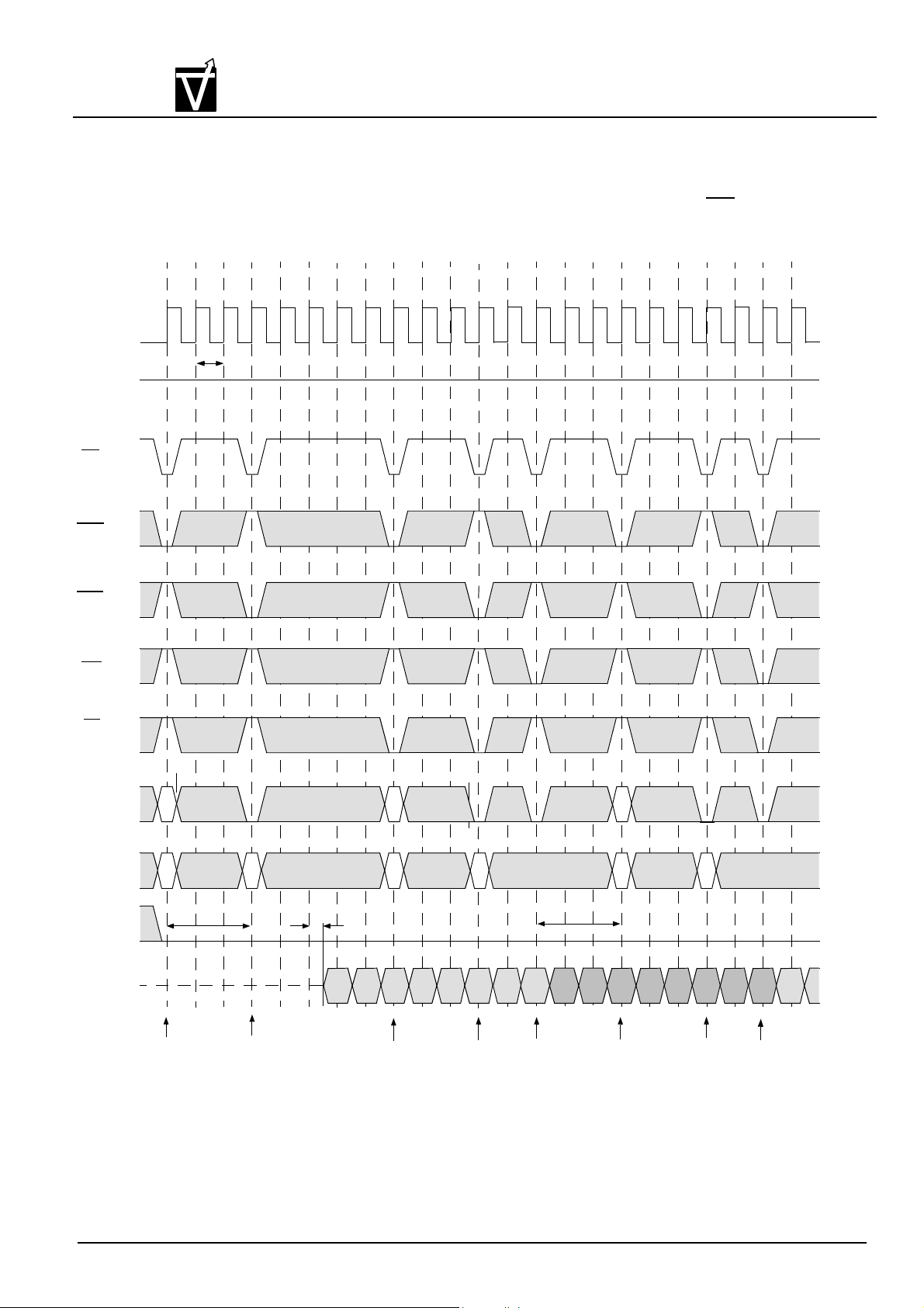
Preliminary VG3664321(4)1(2)BT
VIS
Random Row Read (Interleaving Banks) (2 of 2)
T0 T1 T2 T3 T4 T5 T6 T7 T8 T9 T10 T11 T12 T13 T14 T15 T16 T17 T18 T19 T20 T21 T22
CMOS Synchronous Dynamic RAM
Burst Length = 8, CAS Latency = 3
CLK
CKE
CS
RAS
CAS
WE
BS
High
t
CK3
A10
ADD
t
RCD
t
AC3
t
RP
DQM
DQ
Hi-Z
Activate
Command
Bank B
(Bank D)
Read
Command
Bank B
(Bank D)
QBa2
QBa1
Activate
Command
Bank A
QBa3
QBa5
QBa4
Read
Command
Bank A
QBa6 QBa7
Precharge
Command
Bank B
(Bank D)
QAa0 QAa1
QAa2
Activate
Command
Bank B
(Bank D)
QAa3
QAa4
Command
QAa5
Read
Bank B
(Bank D)
QAa6
QAa7
Precharge
Command
Bank A
Document : 1G5-0099 Rev.1 Page 49
QBb0QBa0
Page 50
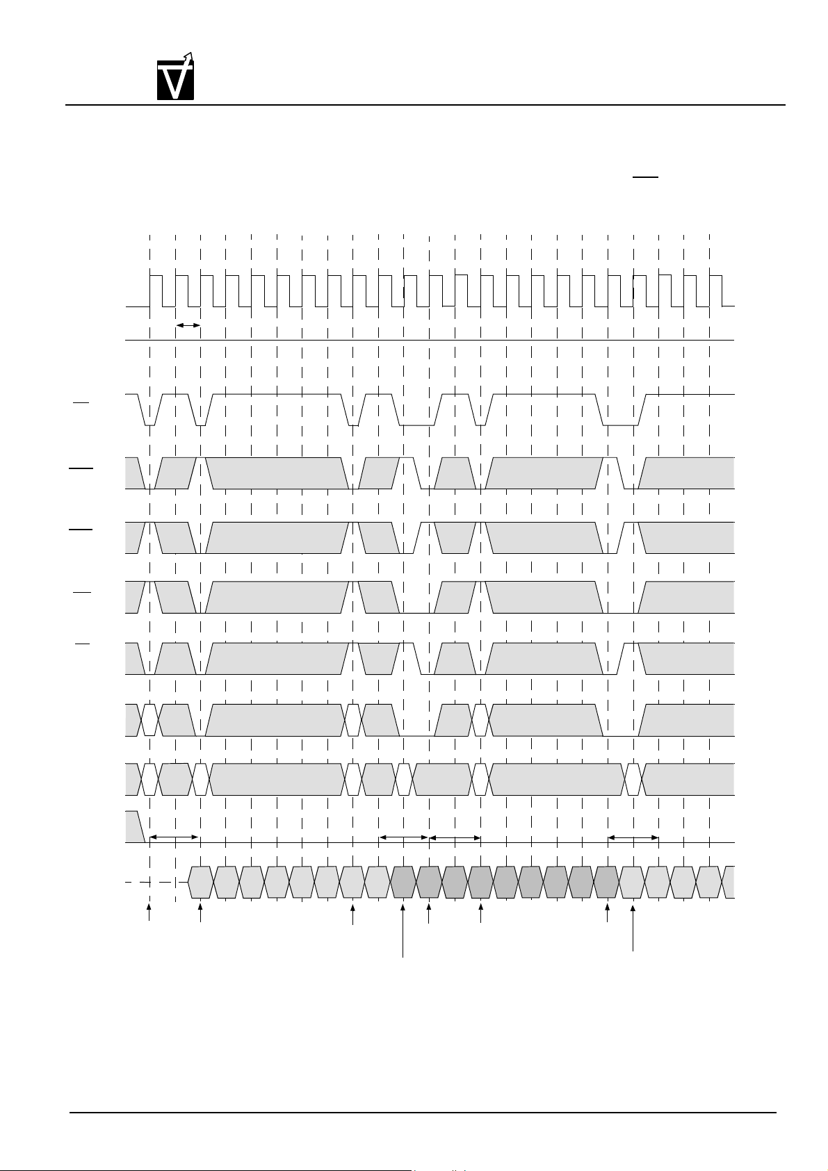
Preliminary VG3664321(4)1(2)BT
VIS
Random Row Write (Interleaving Banks) (1 of 2)
T0 T1 T2 T3 T4 T5 T6 T7 T8 T9 T10 T11 T12 T13 T14 T15 T16 T17 T18 T19 T20 T21 T22
CMOS Synchronous Dynamic RAM
Burst Length = 8, CAS Latency = 2
CLK
CKE
CS
RAS
CAS
WE
BS
High
t
CK2
A10
ADD
DQM
DQ
Hi-Z
Activate
Command
Bank A
t
RCD
Write
Command
Bank A
QAa1 QAa2
QAa3
QAa4
QAa5
QAa6 QAa7
Activate
Command
Bank B
(Bank D)
t
DPL
QBa0 QBa1
Precharge
Command
Bank A
Write
Command
Bank B
(Bank D)
t
RP
QBa2
Command
Bank A
QBa3 QBa4
Active
QBa5
QBa6 QBa7
Command
QAb0 QAb1
Write
Bank A
t
DPL
QAb2QAa0
Precharge
Command
Bank B
(Bank D)
QAb3
Document : 1G5-0099 Rev.1 Page 50
QAb4
Page 51
Preliminary VG3664321(4)1(2)BT
VIS
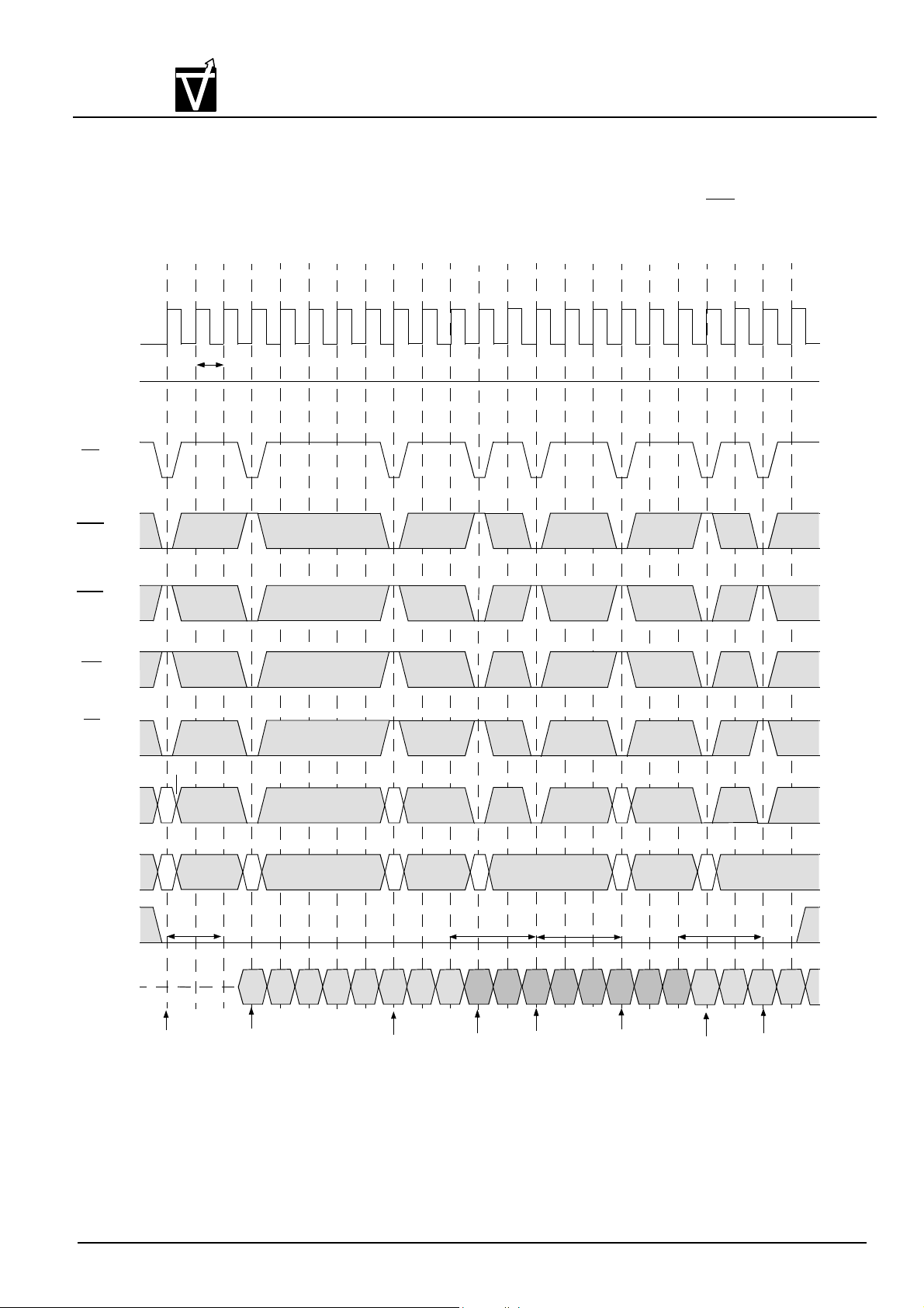
Random Row Write (Interleaving Banks) (2 of 2)
T0 T1 T2 T3 T4 T5 T6 T7 T8 T9 T10 T11 T12 T13 T14 T15 T16 T17 T18 T19 T20 T21 T22
CMOS Synchronous Dynamic RAM
Burst Length = 8, CAS Latency = 3
CLK
CKE
CS
RAS
CAS
WE
BS
High
t
CK3
A10
ADD
DQM
DQ
Hi-Z
Activate
Command
Bank A
t
RCD
QAa0 QAa1
Write
Command
Bank A
QAa2
QAa3
RBa
QAa4
QAa5 QAa6
Activate
Command
Bank B
(Bank D)
QAa7 QBa0
Write
Command
Bank B
(Bank D)
t
DPL
QBa1
Command
QBa2 QBa3
Precharge
Bank A
t
RP
QBa4
QBa5 QBa6
Activate
Command
Bank A
QBb7 QAb0
Write
Command
Bank A
t
DPL
QAb1
QAb2
Precharge
Command
Bank B
(Bank D)
Document : 1G5-0099 Rev.1 Page 51
QAb3
Page 52
Preliminary VG3664321(4)1(2)BT
VIS
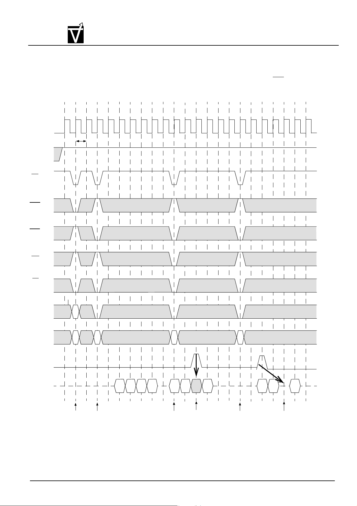
Read and Write Cycle (1 of 2)
T0 T1 T2 T3 T4 T5 T6 T7 T8 T9 T10 T11 T12 T13 T14 T15 T16 T17 T18 T19 T20 T21 T22
CMOS Synchronous Dynamic RAM
Burst Length = 4, CAS Latency = 2
CLK
CKE
CS
RAS
CAS
WE
BS
t
CK2
A10
ADD
RAa
RAa
CAb
CAc CAa
DQM
DQ
Hi-Z
Activate
Command
Bank A
Write
Command
Bank A
QAa0
QAa1
QAa2
QAa3
DAb0
Write
Command
Bank A
DAb1
DAb3 QAc0
The Write Data
is Masked with a
Zero Clock
latency
Read
Command
Bank A
QAc1
The Read Data
is Masked with
Two Clocks
Latency
QAc3
Document : 1G5-0099 Rev.1 Page 52
Page 53
Preliminary VG3664321(4)1(2)BT
VIS
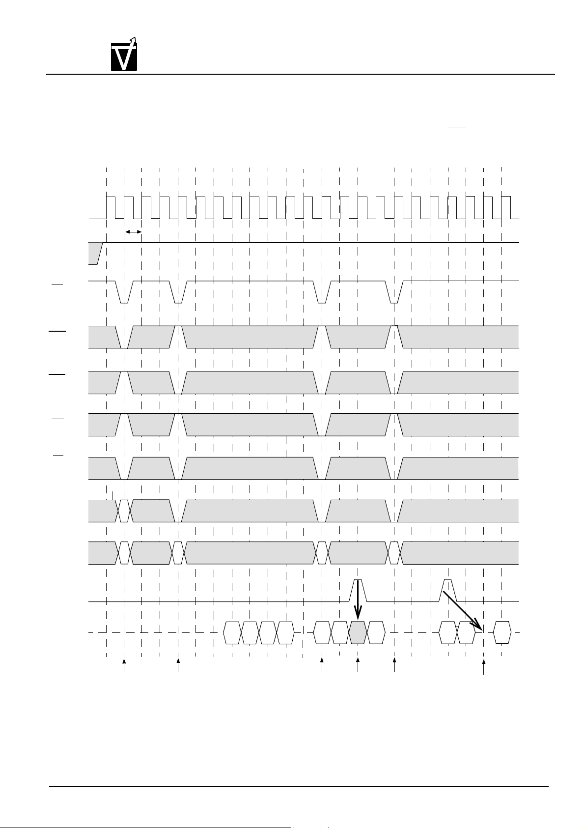
Read and Write Cycle (2 of 2)
T0 T1 T2 T3 T4 T5 T6 T7 T8 T9 T10 T11 T12 T13 T14 T15 T16 T17 T18 T19 T20 T21 T22
CMOS Synchronous Dynamic RAM
Burst Length = 4, CAS Latency = 3
CLK
CKE
CS
RAS
CAS
WE
BS
t
CK3
A10
ADD
RAa
RAa
CAa
CAb
CAc
DQM
DQ
Hi-Z
Activate
Command
Bank A
Read
Command
Bank A
QAa0 QAa1
QAa2
QAa3
DAb0 DAb1
Write
Command
Bank A
DAb3
The Write Data
is Masked with a
Zero Clock
latency
Read
Command
Bank A
QAc0
QAc1
The Read Data
is Masked with
Two Clock
Latency
Document : 1G5-0099 Rev.1 Page 53
QAc3
Page 54
Preliminary VG3664321(4)1(2)BT
VIS
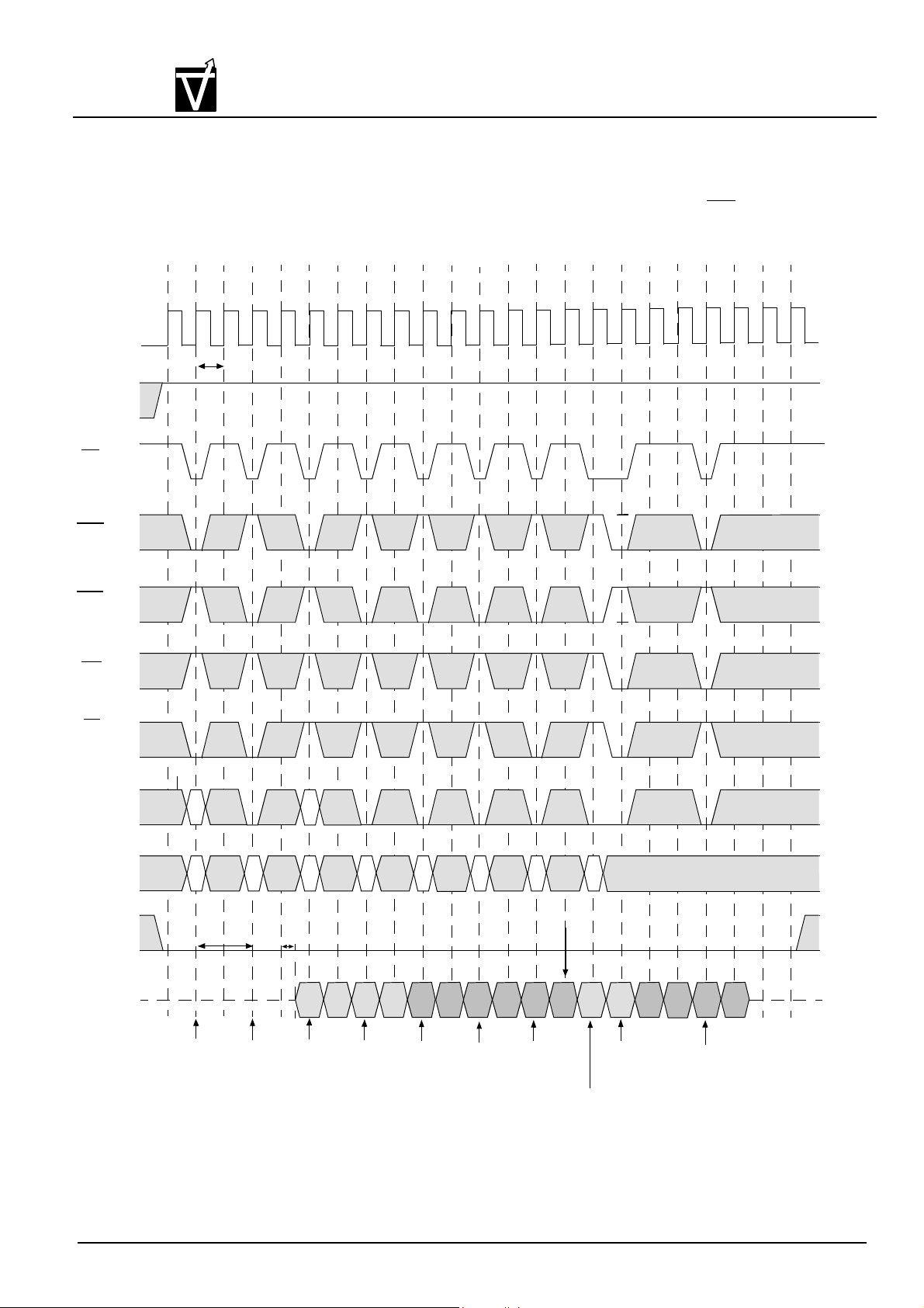
Interleaved Column Read Cycle (1 of 2)
T0 T1 T2 T3 T4 T5 T6 T7 T8 T9 T10 T11 T12 T13 T14 T15 T16 T17 T18 T19 T20 T21 T22
CMOS Synchronous Dynamic RAM
Burst Length = 4, CAS Latency = 2
CLK
CKE
CS
RAS
CAS
WE
BS
t
CK2
A10
ADD
DQM
DQ
Ra Ra
Ra
t
Hi-Z
Activate
Command
Bank A
RCD
Command
Bank A
Cb
Read
Ra
t
AC2
QAa0 QAa1
Activate
Command
Bank B
(Bank D)
Command
Ca Cb Cc Cb Cd
QAa3
QAa2
Read
Bank B
(Bank D)
QBa0
QBa1
Read
Command
Bank B
(Bank D)
QBb0 QAb0
Read
Command
Bank B
(Bank D)
QBc0
QBb1 QBd0
Read
Command
Bank A
QBc1
Command
Bank B
(Bank D)
Read
QAb1
Precharge
Command
Bank A
QBd1
QBd2
QBd3
Precharge
Command
Bank B
(Bank D)
Document : 1G5-0099 Rev.1 Page 54
Page 55
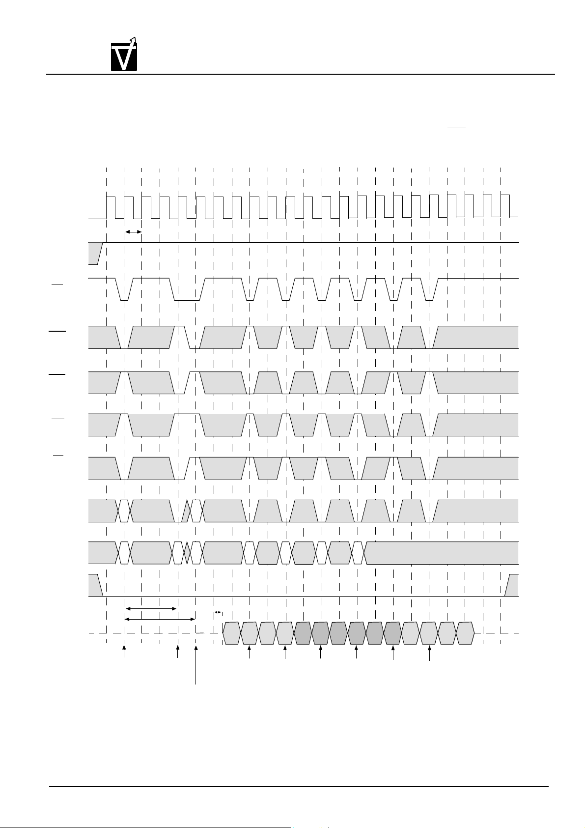
Preliminary VG3664321(4)1(2)BT
VIS
Interleaved Column Read Cycle (2 of 2)
T0 T1 T2 T3 T4 T5 T6 T7 T8 T9 T10 T11 T12 T13 T14 T15 T16 T17 T18 T19 T20 T21 T22
CMOS Synchronous Dynamic RAM
Burst Length = 4, CAS Latency = 3
CLK
CKE
CS
RAS
CAS
WE
BS
t
CK3
A10
ADD
DQM
DQ
Ra Ra
Ra
Hi-Z
Activate
Command
Bank A
t
RCD
t
RRD
Ca
Read
Command
Bank A
Activate
Command
Ra
Bank B
(Bank D)
Ca Cb Cc
t
AC3
QAa1
QAa0
Read
Command
Bank B
(Bank D)
QAa2
Command
QBa0
QAa3
Read
Bank B
(Bank D)
Cb
QBb0 QAb0
QBa1 QAb3
Read
Command
Bank B
(Bank D)
QBc0
QBb1 QAb2
Read
Command
Bank A
QBc1
Precharge
Command
Bank B
(Bank D)
QAb1
Precharge
Command
Bank A
Document : 1G5-0099 Rev.1 Page 55
Page 56
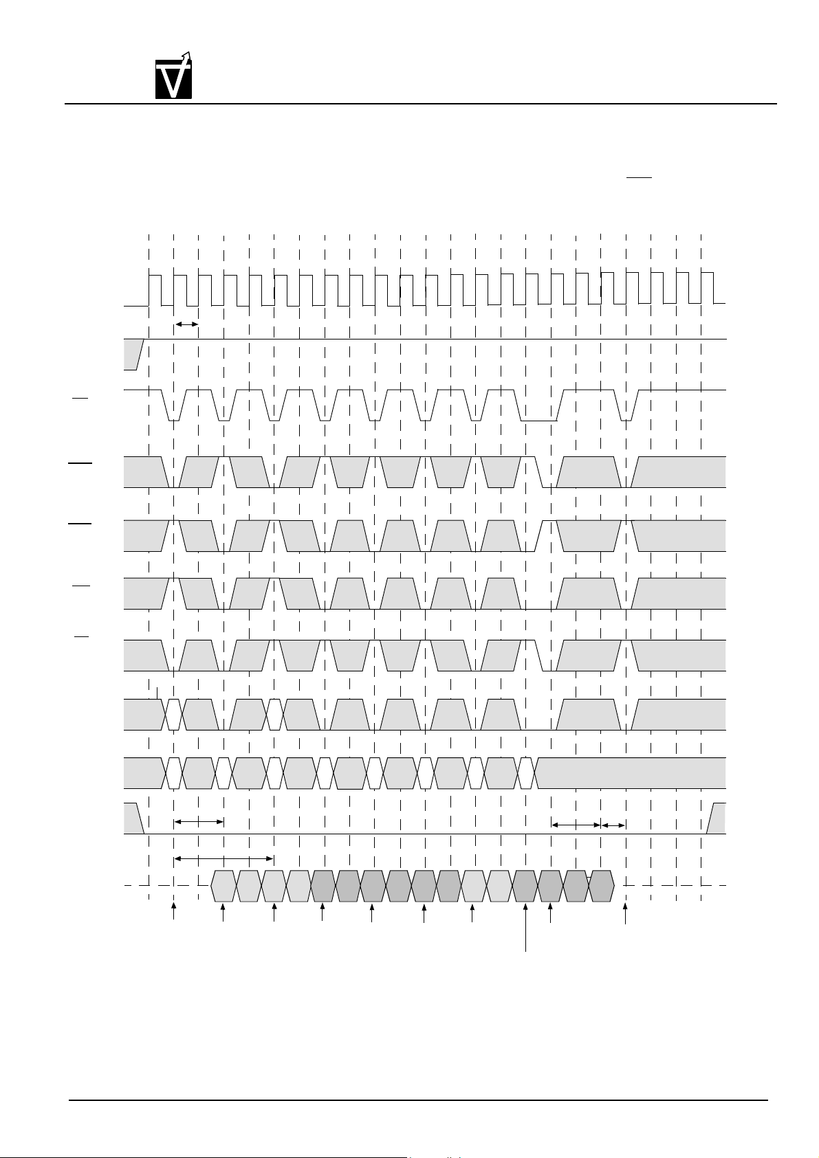
Preliminary VG3664321(4)1(2)BT
VIS
Interleaved Column Write Cycle (1 of 2)
T0 T1 T2 T3 T4 T5 T6 T7 T8 T9 T10 T11 T12 T13 T14 T15 T16 T17 T18 T19 T20 T21 T22
CMOS Synchronous Dynamic RAM
Burst Length = 4, CAS Latency = 2
CLK
CKE
CS
RAS
CAS
WE
BS
t
CK2
A10
ADD
Ra Ra
Ra
t
RCD
Ca
Ra
Ca Cb Cc
Cb
Cb
t
t
RP
DPL
DQM
t
RRD
DQ
Hi-Z
Activate
Command
Bank A
QAa0 QAa1
Write
Command
Bank A
QAa2
Activate
Command
Bank B
(Bank D)
QBa0 QBa1 QBd1
QAa3
Write
Command
Bank B
(Bank D)
QBb0 QAb0
Write
Command
Bank B
(Bank D)
QBb1
QBc0 QBc1
Write
Command
Bank B
(Bank D)
Write
Command
Bank A
QAb1
QBd0
Precharge
Command
Bank A
Write
Command
Bank B
(Bank D)
QBd2 QBd3
Precharge
Command
Bank B
(Bank D)
Document : 1G5-0099 Rev.1 Page 56
Page 57
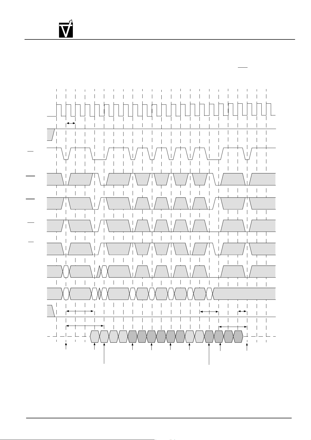
Preliminary VG3664321(4)1(2)BT
VIS
Interleaved Column Write Cycle (2 of 2)
T0 T1 T2 T3 T4 T5 T6 T7 T8 T9 T10 T11 T12 T13 T14 T15 T16 T17 T18 T19 T20 T21 T22
CMOS Synchronous Dynamic RAM
Burst Length = 4, CAS Latency = 3
CLK
CKE
CS
RAS
CAS
WE
BS
t
CK3
A10
ADD
Ra Ra
Ra
Ra
t
Ca
RCD
Ca Cb Cc
Cb
t
DPL
Cd
t
DPL
DQM
DQ
Hi-Z
Activate
Command
Bank A
t
RRD
DAa0 DAa1
Write
Command
Bank A
Activate
Command
Bank B
(Bank D)
DAa2
DAa3
Command
DBa0 DBa1
Write
Bank B
(Bank D)
DBb0 DAb0
Write
Command
Bank B
(Bank D)
DBc0 DBc1
DBb1 DAd0
Write
Command
Bank B
(Bank D)
Write
Command
Bank A
DAb1
Write
Command
Bank B
(Bank D)
QAd1
QAd2 QAd3
Precharge
Command
Bank A
t
RP
Precharge
Command
Bank B
(Bank D)
Document : 1G5-0099 Rev.1 Page 57
Page 58
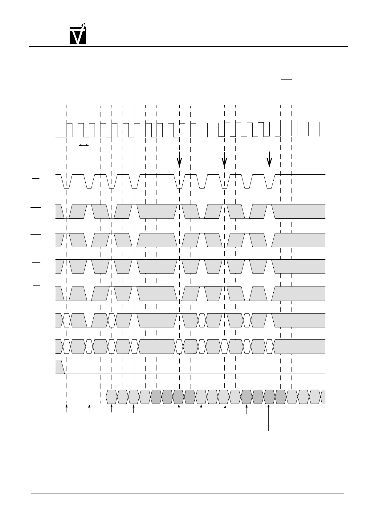
Preliminary VG3664321(4)1(2)BT
VIS
Auto Precharge after Read Burst (1 of 2)
T0 T1 T2 T3 T4 T5 T6 T7 T8 T9 T10 T11 T12 T13 T14 T15 T16 T17 T18 T19 T20 T21 T22
CMOS Synchronous Dynamic RAM
Burst Length = 4, CAS Latency = 2
CLK
CKE
CS
RAS
CAS
WE
BS
High
t
CK2
Start Auto Precharge
Bank B (Bank D)
Start Auto Precharge
Bank A
Start Auto Precharge
Bank B (Bank D)
A10
ADD
Ra Ra
Ra
Ca
Ra
Ca Cb Rb
Rb Rc
Cb
Rc
Cc
DQM
DQ
Hi-Z
Activate
Command
Bank A
Read
Command
Bank A
QAa0
Activate
Command
Bank B
(Bank D)
QAa1
QAa2
Read with
Auto Precharge
Command
Bank B
(Bank D)
QAa3
QBa0
QBa2 QAb2
QBa1 QBb1
Read with
Auto Precharge
Command
Bank A
QAb0
QBa3 QBb0
QAb1
Activate
Command
Bank B
(Bank D)
QAb3
Read with
Auto Precharge
Command
Bank B
(Bank D)
Activate
Command
Bank A
QBb2 QBb3
Read with
Auto Precharge
Command
Bank A
QAc1
QAc0 QAc2
Document : 1G5-0099 Rev.1 Page 58
Page 59
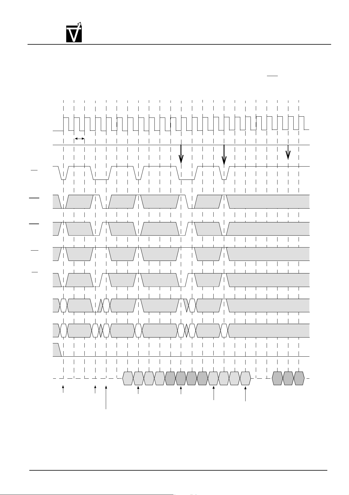
Preliminary VG3664321(4)1(2)BT
VIS
Auto Precharge after Read Burst (2 of 2)
T0 T1 T2 T3 T4 T5 T6 T7 T8 T9 T10 T11 T12 T13 T14 T15 T16 T17 T18 T19 T20 T21 T22
CMOS Synchronous Dynamic RAM
Burst Length = 4, CAS Latency = 3
CLK
CKE
CS
RAS
CAS
WE
BS
High
t
CK3
Start Auto Precharge
Bank B (Bank D)
Start Auto Precharge
Bank A
Start Auto Precharge
Bank B (Bank D)
A10
ADD
RAa
RAa
RBa
RBa
CBa
CAb
RBb
RBb
CBbCAa
DQM
DQ
Hi-Z
Activate
Command
Bank A
Read
Command
Bank A
Activate
Command
Bank B
(Bank D))
QAa0 QAa1
Read with
Auto Precharge
Command
Bank B
(Bank D)
QAa2
QAa3
QBa0
QAb0
QBa1 QBb1
Read with
Auto Precharge
Command
Bank A
QBa3 QBb0
QBa2 QAb2
Activate
Command
Bank B
(Bank D)
QAb1
QAb3
Read with
Auto Precharge
Command
Bank B (Bank D)
Document : 1G5-0099 Rev.1 Page 59
QBb2
Page 60
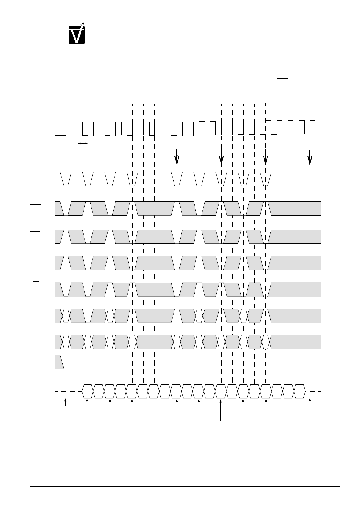
Preliminary VG3664321(4)1(2)BT
VIS
Auto Precharge after Write Burst (1 of 2)
T0 T1 T2 T3 T4 T5 T6 T7 T8 T9 T10 T11 T12 T13 T14 T15 T16 T17 T18 T19 T20 T21 T22
CMOS Synchronous Dynamic RAM
Burst Length = 4, CAS Latency = 2
CLK
CKE
CS
RAS
CAS
WE
BS
High
t
CK2
Start Auto Precharge
Bank B
Start Auto Precharge
Bank A
Start Auto Precharge
Bank B
A10
ADD
RAa
RAa
RBa
RBa
CBa
CAb
RBb
RBb
RAc
CBbCAa
RAc CAc
DQM
DQ
Hi-Z
Activate
Command
Bank A
QAa0 QAa1
Write
Command
Bank A
QAa3
QAa2
Activate
Command
Bank B
(Bank D)
QBa0 QBa1 QBb1
Write with
Auto Precharge
Command
Bank B
(Bank D)
QBa2 QAb2
QAb0 QAb1
QBa3
Write with
Auto Precharge
Command
Bank A
Activate
Command
Bank B
(Bank D)
QBb0
QAb3
Write with
Auto Precharge
Command
Bank B
(Bank D)
QBb2 QBb3
Activate
Command
Bank A
QAc0 QAc1 QAc2 QAc3
Write with
Auto Precharge
Bank A
Start Auto
Precharge
Document : 1G5-0099 Rev.1 Page 60
Bank A
Page 61
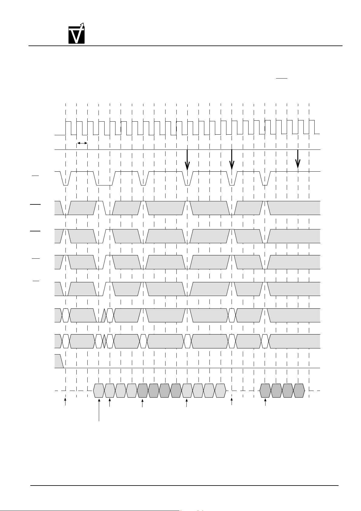
Preliminary VG3664321(4)1(2)BT
VIS
Auto Precharge after Write Burst (2 of 2)
T0 T1 T2 T3 T4 T5 T6 T7 T8 T9 T10 T11 T12 T13 T14 T15 T16 T17 T18 T19 T20 T21 T22
CMOS Synchronous Dynamic RAM
Burst Length = 4, CAS Latency = 3
CLK
CKE
CS
RAS
CAS
WE
BS
High
t
CK3
Start Auto Precharge
Bank B (Bank D)
Start Auto Precharge
Bank A
Start Auto Precharge
Bank B (Bank D)
A10
ADD
Ra
Ra
Ca
Ra
Ra
Ca
Cb
Rb
Rb
Cb
DQM
DQ
Hi-Z
Activate
Command
Bank A
QAa0 QAa1
Activate
Command
Bank B
(Bank D)
Write
Command
Bank A
QAa2
QBa0
QAa3
Write with
Auto Precharge
Command
Bank B
(Bank D)
QAb0
QBa1
QBa3
QBa2 QAb2
Write with
Auto Precharge
Command
Bank A
QAb1
QAb3
Command
Activate
Bank B
(Bank D)
QBb0
QBb1 QBb2 QBb3
Write with
Auto precharge
Command
Bank B
(Bank D)
Document : 1G5-0099 Rev.1 Page 61
Page 62
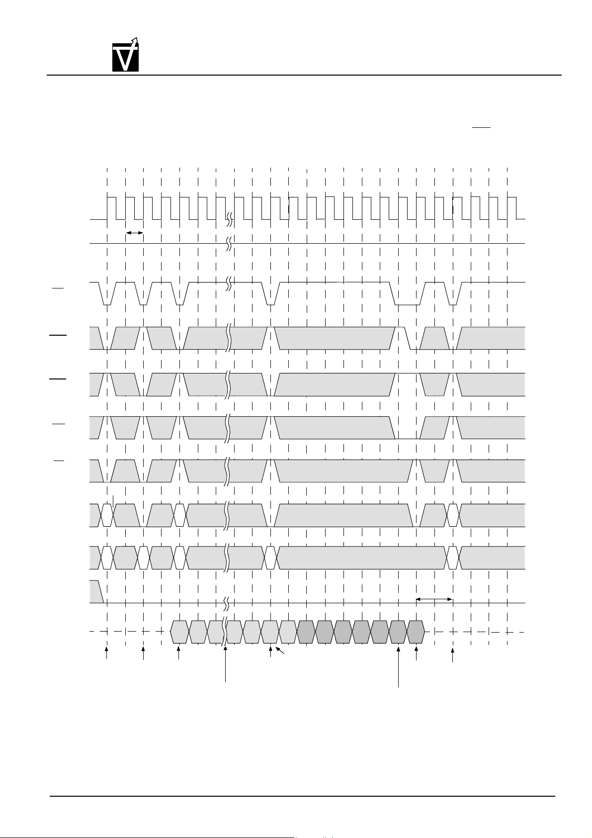
Preliminary VG3664321(4)1(2)BT
VIS
Full Page Read Cycle (1 of 2)
T0 T1 T2 T3 T4 T5 T6 T7 T8 T9 T10 T11 T12 T13 T14 T15 T16 T17 T18 T19 T20 T21 T22
CMOS Synchronous Dynamic RAM
Burst Length = Full Page, CAS Latency = 2
CLK
CKE
CS
RAS
CAS
WE
BS
High
t
CK2
A10
ADD
DQM
DQ
Ra
Ra
Hi-Z
Activate
Command
Bank A
Ra
QAa-1
Command
Bank B
(Bank D)
Ca
QAa+1 QBa QBa+1
QAa
Full page burst operation does not
Read
terminate when the burst length is
satisfied; the burst counter
increments and continues bursting
beginning with the starting address
QBa+2
QBa+3
QBa+4 QBa+51
Burst Stop
Command
QBa+6
Precharge
Command
Bank B
(Bank D)
Ca Rb
Read
Command
Bank A
Ra
QAa
Activate
Command
Bank B
(Bank D)
QAa+1
QAa+2
QAa-2
The burst counter wraps
from the highest order
page address back to zero
during this time interval
t
RP
Rb
Activate
Command
Bank B
(Bank D)
Document : 1G5-0099 Rev.1 Page 62
Page 63
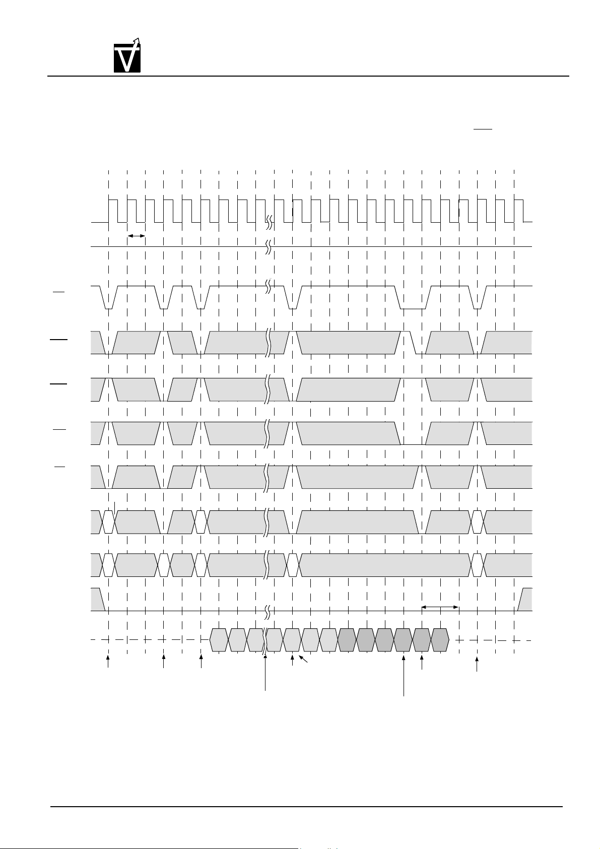
Preliminary VG3664321(4)1(2)BT
VIS
Full Page Read Cycle (2 of 2)
T0 T1 T2 T3 T4 T5 T6 T7 T8 T9 T10 T11 T12 T13 T14 T15 T16 T17 T18 T19 T20 T21 T22
CMOS Synchronous Dynamic RAM
Burst Length = Full Page, CAS Latency = 3
CLK
CKE
CS
RAS
CAS
WE
BS
High
t
CK3
A10
ADD
DQM
DQ
Ra
Ra
Hi-Z
Activate
Command
Bank A
Ra
QAa-2
Read
Command
Bank B
(Bank D)
Ca
QAa+1
QAa
QAa-1
Full page burst operation
does not teminate when
the burst length is satisfied;
the burst counter increments
and continues bursting
beginning with the starting
address
QBa0
QBa+1
QBa+2
QBa+3
Precharge
Command
Bank B
(Bank D)
Burst Stop
Command
QBa+4
t
RP
QBa+5
Ca Rb
Read
Command
Bank A
Ra
Activate
Command
Bank B
(Bank D)
QAa+2
QAa+1
QAa
The burst counter wraps
from the highest order
page address back to zero
during this time interval
Rb
Activate
Command
Bank B
(Bank D)
Document : 1G5-0099 Rev.1 Page 63
Page 64
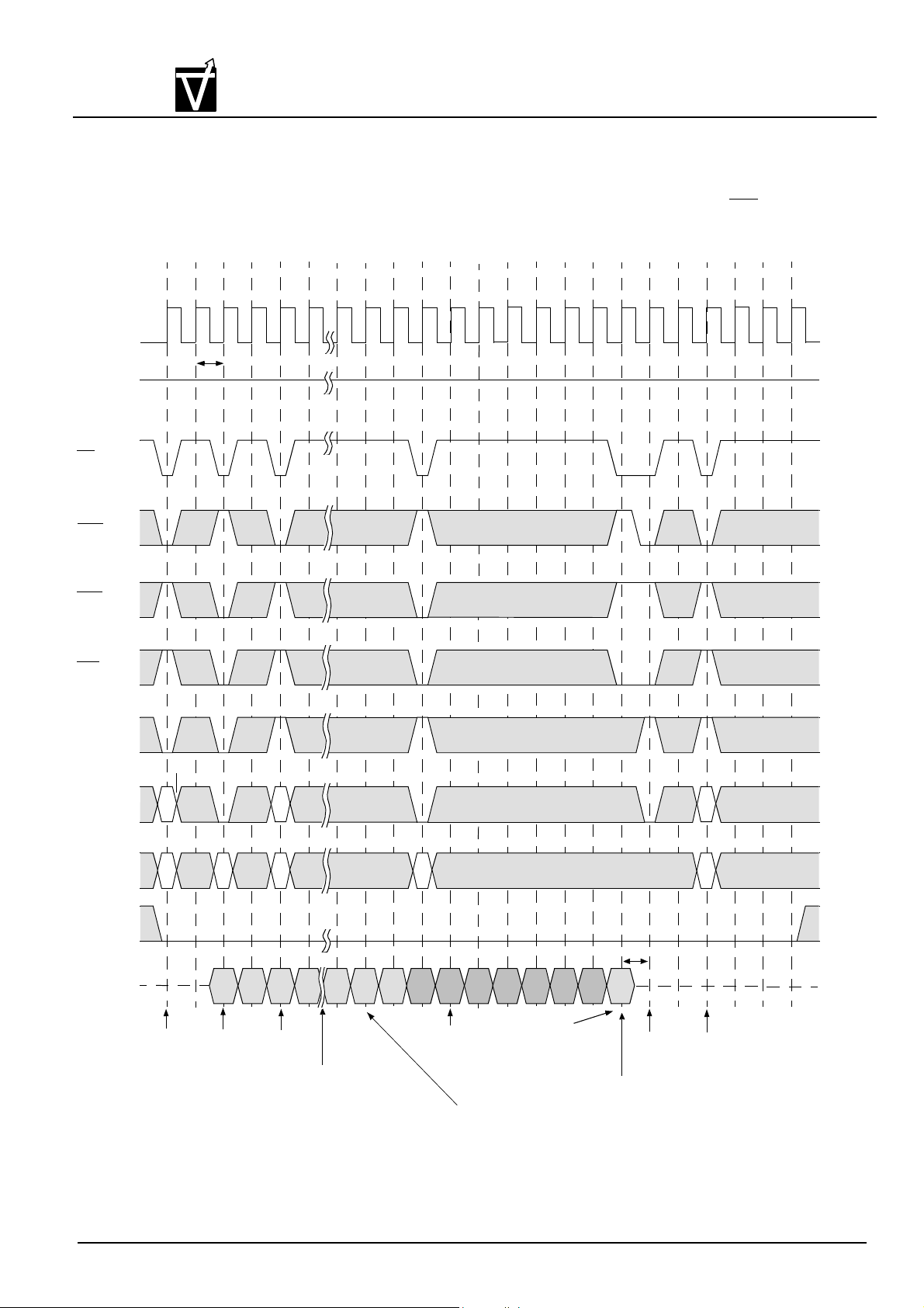
Preliminary VG3664321(4)1(2)BT
VIS
Full Page Write Cycle (1 of 2)
T0 T1 T2 T3 T4 T5 T6 T7 T8 T9 T10 T11 T12 T13 T14 T15 T16 T17 T18 T19 T20 T21 T22
CMOS Synchronous Dynamic RAM
Burst Length = Full Page, CAS Latency = 2
CLK
CKE
CS
RAS
CAS
WE
A11(BS)
High
t
CK2
A10
A0~A9
DDM
DQ
Ra
Ra
Hi-Z
Activate
Command
Bank A
Ra
Ca Rb
QAa
Write
Command
Bank A
Ra
QAa+1
QAa+2 QAa+3
Activate
Command
Bank B
(Bank D)
The burst counter wraps
from the highest order
page address back to zero
during this time interval
QAa-1
QAa
QAa+1
Ca
QBa
Command
Bank B
(Bank D)
QBa+1
QBa+2
DQBa+3
Write
Full page burst operation
does not terminate when
the burst length is satisfied;
the burst counter increments
and continues bursting
beginning with the starting
address
QBa+4
Data is ignored
QBa+5
QBa+6
t
BDL
Precharge
Command
Bank B
(Bank D)
Burst Stop
Command
Rb
Activate
Command
Bank B
(Bank D)
Document : 1G5-0099 Rev.1 Page 64
Page 65
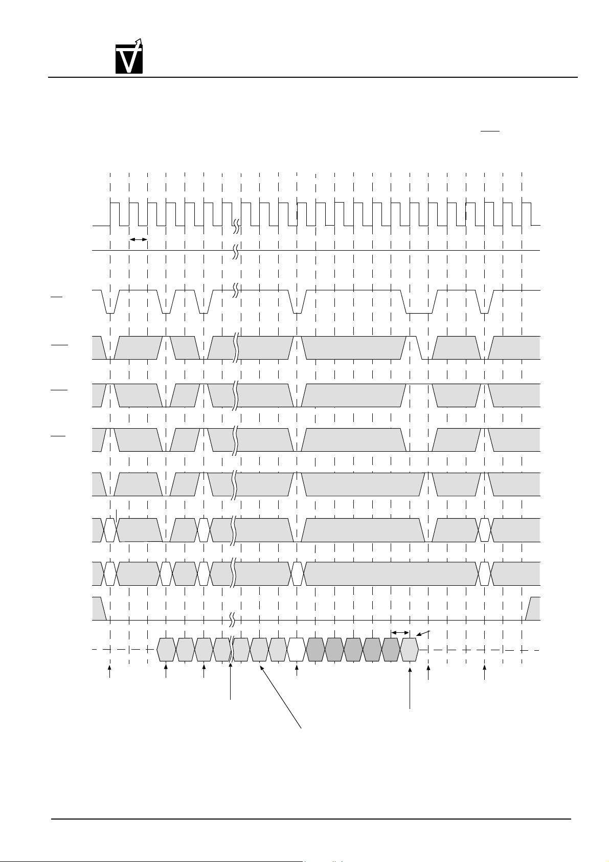
Preliminary VG3664321(4)1(2)BT
VIS
Full Page Write Cycle (2 of 2)
T0 T1 T2 T3 T4 T5 T6 T7 T8 T9 T10 T11 T12 T13 T14 T15 T16 T17 T18 T19 T20 T21 T22
CMOS Synchronous Dynamic RAM
Burst Length = Full Page, CAS Latency = 3
CLK
CKE
CS
RAS
CAS
WE
A11(BS)
High
t
CK3
A10
A0~A9
DDM
DQ
Ra
Ra
Hi-Z
Activate
Command
Bank A
Ca
DAa
Write
Command
Bank A
Ra
Ra
DAa+1
DAa+2 DAa+3
Activate
Command
Bank B
(Bank D)
The burst counter wraps
from the highest order
page address back to zero
during this time interval
DAa-1
DAa
DAa+1
Command
Ca
DBa+1 DBa+2
DBa
Write
Bank B
(Bank D)
Full page burst operation
does not terminate when
the burst length is satisfied;
the burst counter increments
and continues bursting
beginning with the starting
address
DBa+3
DBa+4
DBa+5
t
BDL
Burst Stop
Command
Data is ignored.
Precharge
Command
Bank B
(Bank D)
Rb
Rb
Activate
Command
Bank B
(Bank D)
Document : 1G5-0099 Rev.1 Page 65
Page 66
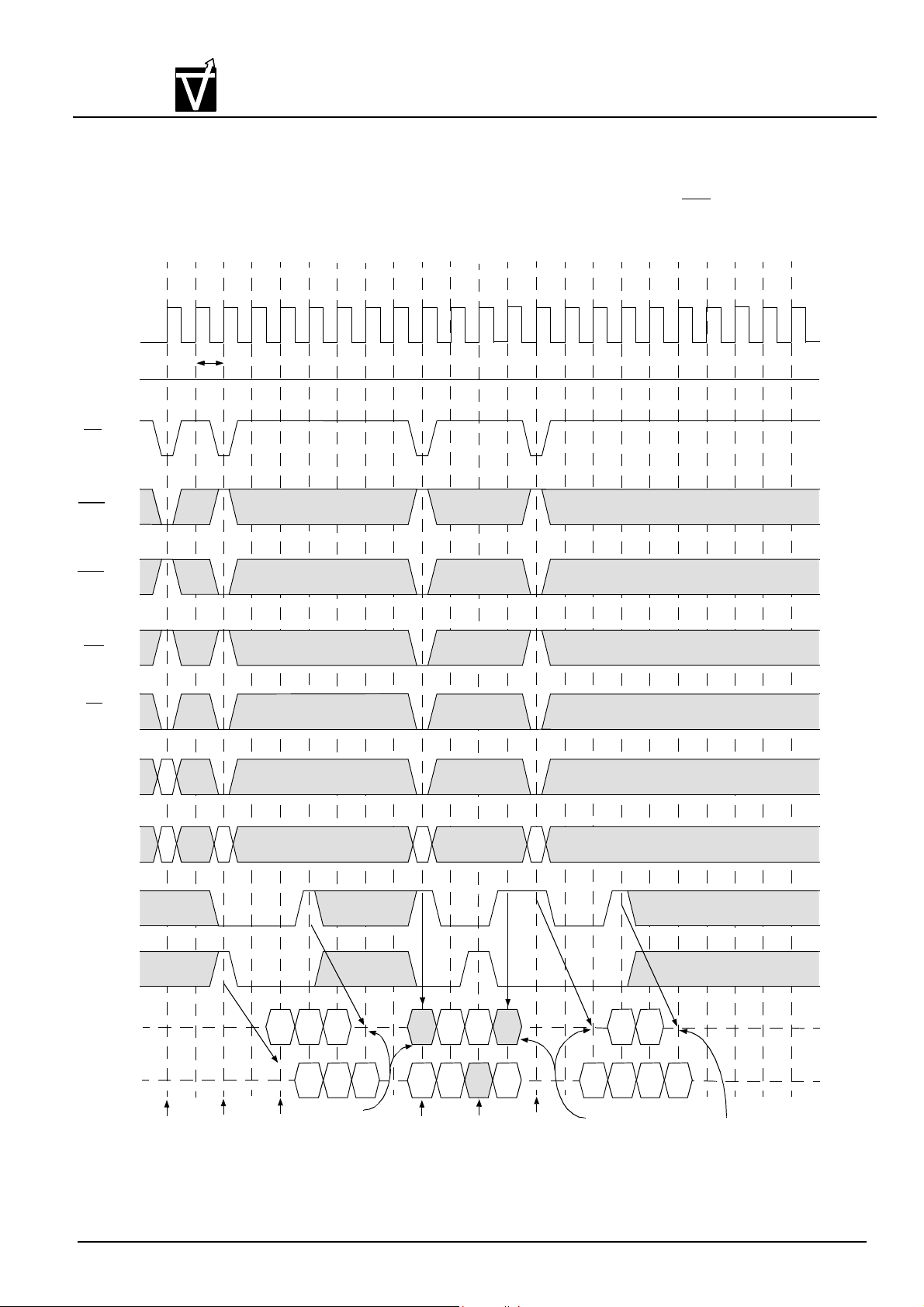
VIS
Byte Write Operation
T0 T1 T2 T3 T4 T5 T6 T7 T8 T9 T10 T11 T12 T13 T14 T15 T16 T17 T18 T19 T20 T21 T22
Preliminary VG3664321(4)1(2)BT
CMOS Synchronous Dynamic RAM
Burst Length = 4, CAS Latency = 2
CLK
CKE
CS
RAS
CAS
WE
BS
A10
High
RAa
t
CK2
ADD
RAa
CAa
CAb
CAz
DQM
DQ
DQ0 ~ DQ7
DQ8 ~ DQ15
Hi-Z
Hi-Z
Activate
Command
Bank A
Read
Command
Bank A
Upper Byte
is masked
Lower Byte
is masked
Write
Command
Bank A
Write Upper
is masked
Read
Command
Bank A
Lower Byte
is masked
Lower Byte
is masked
Document : 1G5-0099 Rev.1 Page 66
Page 67
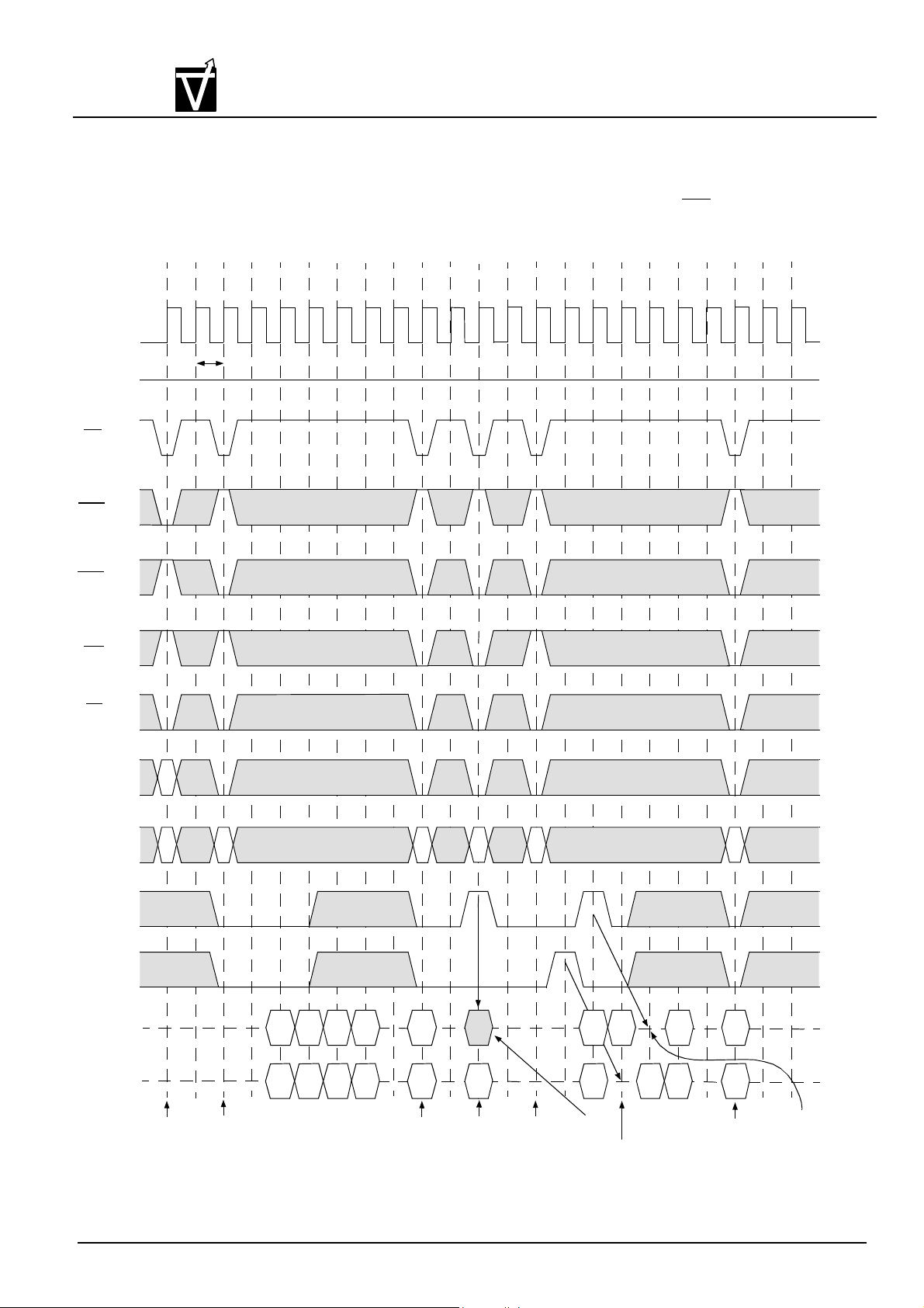
Preliminary VG3664321(4)1(2)BT
VIS
Burst Read and Single Write Operation
T0 T1 T2 T3 T4 T5 T6 T7 T8 T9 T10 T11 T12 T13 T14 T15 T16 T17 T18 T19 T20 T21 T22
CMOS Synchronous Dynamic RAM
Burst Length = 4, CAS Latency = 2
CLK
CKE
CS
RAS
CAS
WE
BS
A10
High
RAa
t
CK2
ADD
RAa
CAa
CAb
CAc CAe
CAd
DQM
DQ
DQ0 ~ DQ7
DQ8 ~ DQ15
Hi-Z
Hi-Z
Activate
Command
Bank A
Read
Command
Bank A
Single Write
Command
Bank A
Single Write
Command
Bank A
Read
Command
Bank A
Lower Byte
is masked
Upper Byte
is masked
Single Write
Command
Bank A
Document : 1G5-0099 Rev.1 Page 67
Lower Byte
is masked
Page 68
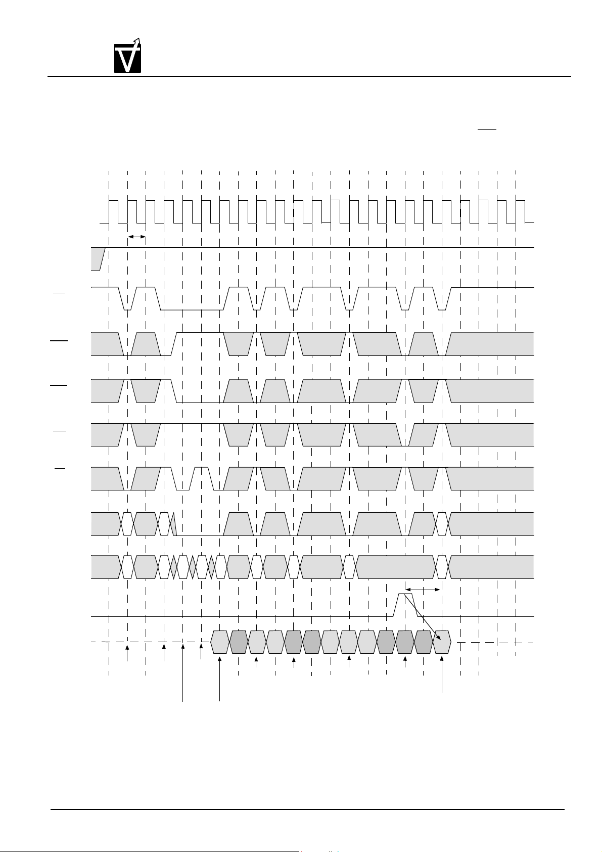
Preliminary VG3664321(4)1(2)BT
VIS
Full Page Random Column Read
T0 T1 T2 T3 T4 T5 T6 T7 T8 T9 T10 T11 T12 T13 T14 T15 T16 T17 T18 T19 T20 T21 T22
CMOS Synchronous Dynamic RAM
Burst Length = Full Page, CAS Latency = 2
CLK
CKE
CS
RAS
CAS
WE
BS
t
CK2
A10
ADD
Ra
Ra
Ra
Ra Ca Ca
Cb Cb
Cc Cc Rb
t
RP
Rb
DQM
DQ
Hi-Z
Activate
Command
Bank A
Activate
Command
Bank B
(Bank D)
Command
Read
Bank A
Read
Command
Bank B
(Bank D)
Command
QAa0
Read
Bank A
QBa0
Read
Command
Bank B
(Bank D)
QAb0 QAb1
QBb0
Read
Command
Bank A
QBb1 QAc0
Command
QAc1
Read
Bank B
(Bank D)
QAc2
Command Bank B (Bank D)
QBc1 QBc2
QBc0
Precharge
(Precharge Termination)
Activate
Command
Bank B
(Bank D)
Document : 1G5-0099 Rev.1 Page 68
Page 69
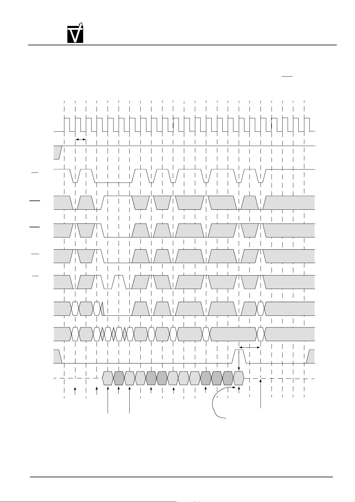
Preliminary VG3664321(4)1(2)BT
VIS
Full Page Random Column Write
T0 T1 T2 T3 T4 T5 T6 T7 T8 T9 T10 T11 T12 T13 T14 T15 T16 T17 T18 T19 T20 T21 T22
CMOS Synchronous Dynamic RAM
Burst Length = Full Page, CAS Latency = 2
CLK
CKE
CS
RAS
CAS
WE
BS
t
CK2
A10
ADD
Ra
Ra
Ra
Ra Ca Ca
Cb Cb
Cc Cc Rb
t
RP
Rb
DQM
DQ
Hi-Z
Activate
Command
Bank A
Activate
Command
Bank B
(Bank D)
Command
QAa0
Write
Bank A
QBa0
Write
Command
Bank B
(Bank D)
Command
QAb0
Write
Bank A
QAb1
QBb0 QBb1
Write
Command
Bank B
(Bank D)
QAc0
Write
Command
Bank A
QAc1
QAc2
Command
Bank B
(Bank D)
QBc1
QBc0
Write
Command Bank B (Bank D)
(Precharge Termination)
QBc2
Precharge
Write Data
is masked
Activate
Command
Bank B
(Bank D)
Document : 1G5-0099 Rev.1 Page 69
Page 70
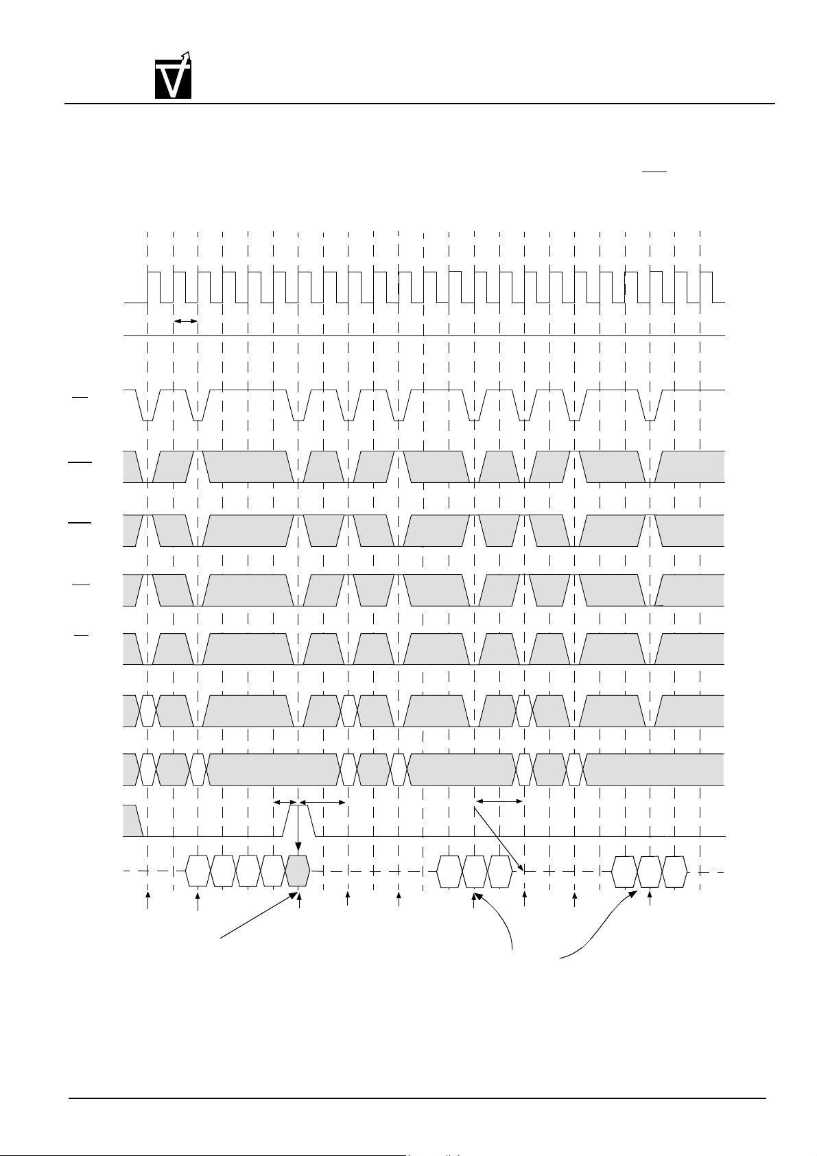
Preliminary VG3664321(4)1(2)BT
VIS
Precharge Termination of a Burst (1 of 2)
T0 T1 T2 T3 T4 T5 T6 T7 T8 T9 T10 T11 T12 T13 T14 T15 T16 T17 T18 T19 T20 T21 T22
CMOS Synchronous Dynamic RAM
Burst Length = 4,8 or Full Page, CAS Latency = 2
CLK
CKE
CS
RAS
CAS
WE
BS
High
t
CK2
A10
ADD
RAa
RAa CAcCAa
t
DPLtRP
RAb
RAb
t
RAc
RAc CAb
RP
DQM
DQ
Hi-Z
Activate
Command
Bank A
QAa0
QAa1 QAa2
Write
Command
Bank A
Precharge Termination
of a Write Burst.Write
data is masked.
QAa3
Precharge
Command
Bank A
Activate
Command
Bank A
Read
Command
Bank A
QAc2QAb0
QAc1
Precharge
Command
Bank A
Activate
Command
Precharge Termination
of a Read Burst.
Bank A
Read
Command
Bank A
QAc1
Precharge
Command
Bank A
QAc2QAb0
Document : 1G5-0099 Rev.1 Page 70
Page 71
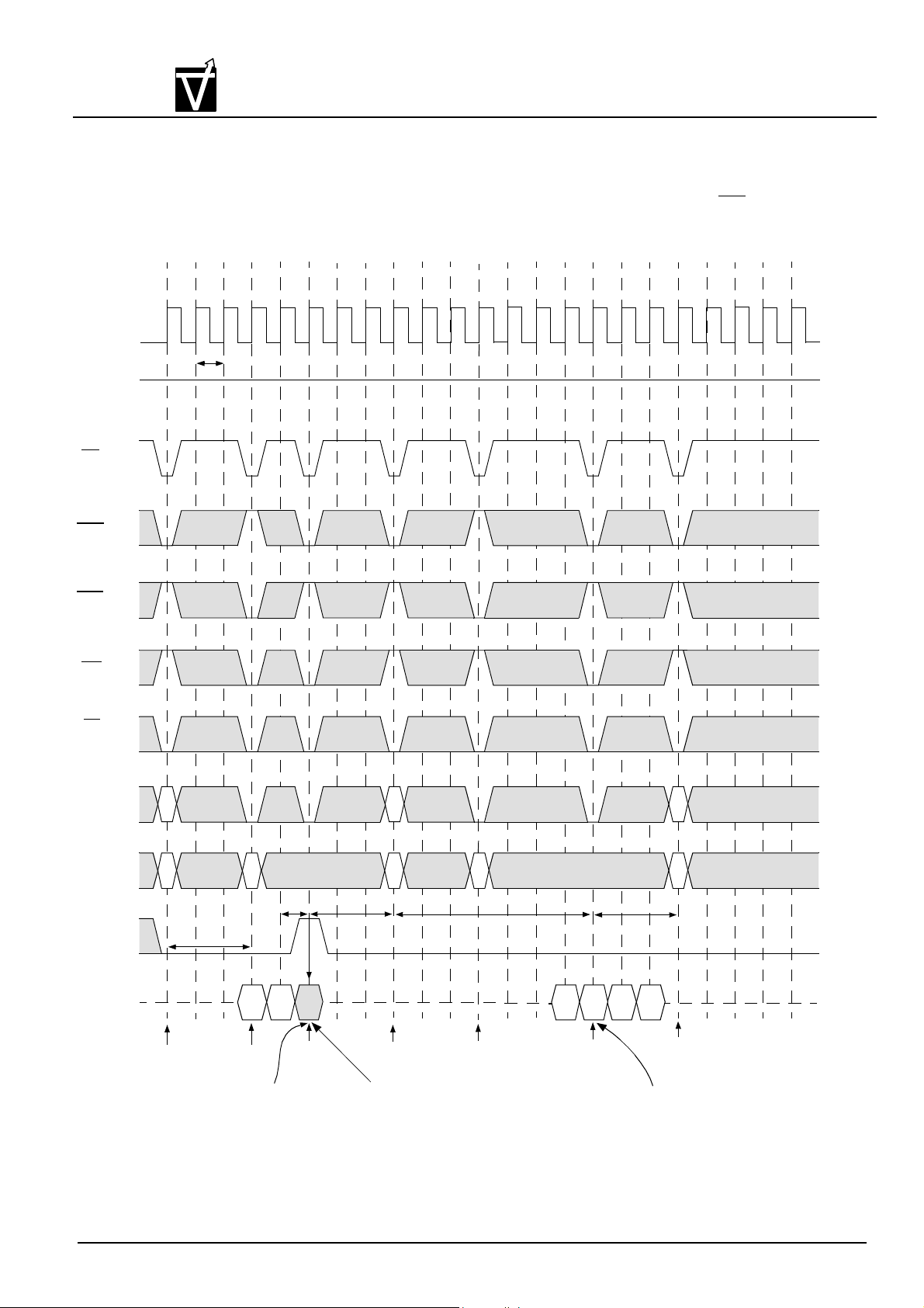
Preliminary VG3664321(4)1(2)BT
VIS
Precharge Termination of a Burst (2 of 2)
T0 T1 T2 T3 T4 T5 T6 T7 T8 T9 T10 T11 T12 T13 T14 T15 T16 T17 T18 T19 T20 T21 T22
CMOS Synchronous Dynamic RAM
Burst Length=4,8 or Full Page, CAS Latency=3
CLK
CKE
CS
RAS
CAS
WE
BS
High
t
CK3
A10
ADD
DQM
DQ
RAa
RAa RAcCAa
t
RCD
Hi-Z
Activate
Command
Bank A
Write
Command
Bank A
Write Data
is masked
t
DPL
DAa1DAa0
Precharge
Command
Bank A
Precharge Termination
of a Write Burst.
t
RP
RAb
RAb
Activate
Command
Bank A
CAb
t
Read
Command
Bank A
RAS
QAb0 QAb1
Precharge
Command
Bank A
RAc
t
RP
QAb2 QAb3
Activate
Command
Bank A
Precharge Termination
of a Read Burst.
Document : 1G5-0099 Rev.1 Page 71
Page 72
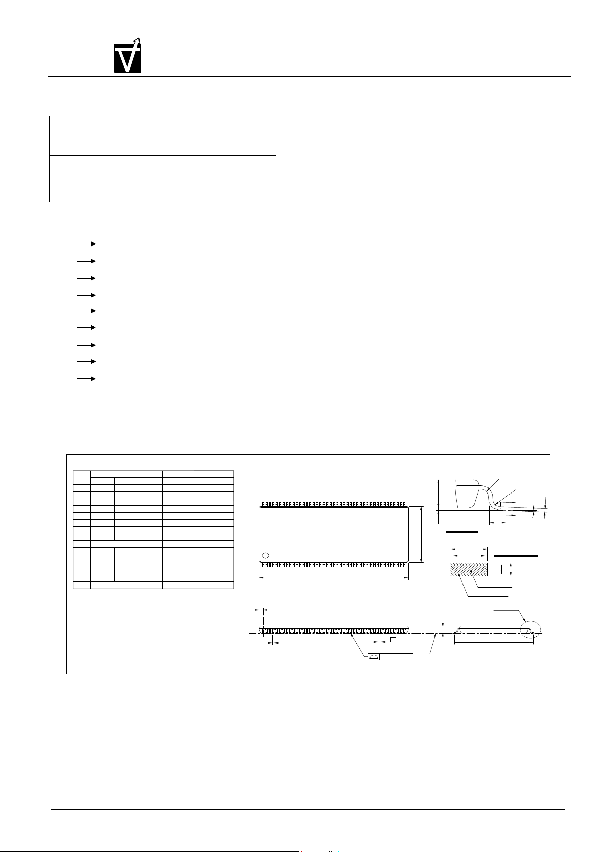
Preliminary VG3664321(4)1(2)BT
VIS
Ordering information
Part Number Cycle time Package
VG36643241BT-7 7ns 400mil
CMOS Synchronous Dynamic RAM
VG36643241BT-8 8ns
VG36643241BT-10 10ns
VG36643211BT-8
• VG
• 36
• 64
• 32
• 1
• 1
• B
• T
• 8
•
VIS Memory Product
•
Technology/Design Rule
•
64Mb
•
Device Configuration, 32 : x32
•
Device Internal Banks, 1 : 2banks, 4 : 4banks
•
Interface Type, 1 : LVTTL, 2 : SSTL-3
•
Mask/Design Version
•
Package Type, T : TSOP
•
Cycle time, 10 : 10ns, 8 : 8ns, 7 : 7ns
Packaging Information
• 400mil, 86-Pin Plastic TSOP
44-Pin
Plastic TSOP
10.03E1
L 0.40
R 0.12
MILLIMETERS
MIN.
0.05
0.17b
22.09D
0.12
0.50 BASIC
MAX.
NOM.
1.20
---
0.15
---
1.05
1.00
0.27
---
0.23
0.20
0.21
---
0.16
0.125 0.005
22.3522.22
11.9611.76 0.455
10.2910.16 0.395
0.60
0.50
0.25
---
---
0.61 REF.
MIN.
---
0.002
0.037
0.007
0.007
(0.005)
(0.005)
0.870
0.016
0.005
0.0050.12
---
DIM
AA1---
A2 0.95
b1 0.17
c1c0.12
e
E 11.56
R1
ZD
NOTE:
1. CONTROLLING DIMENSION : MILLIMETERS
2. DIMENSION D DOES NOT INCLUDE MOLD PROTRUSION.
MOLD PROTRUSION SHALL NOT EXCEED 0.15mm(0.006") PER SIDE.
DIMENSION E1 DOES NOT INCLUDE INTERLEAD PROTRUSION.
INTERLEAD PROTRUSION SHALL NOT EXCEED 0.25mm(0.01") PER SIDE.
3. DIMENSION b DOES NOT INCLUDE DAMBAR PROTRUSIONS/INTRUSION.
ALLOWABLE DAMBAR PROTRUSION SHALL NOT CAUSE THE LEAD TO
BE WIDER THAN THE MAX b DIMENSION BY MORE THAN 0.13mm.
DAMBAR INTRUSION SHALL NOT CAUSE THE LEAD TO BE NARROWER
THAN THE MIN b DIMENSION BY MORE THAN 0.07mm.
INCHES
NOM.
---
---
0.039
---
0.008
---
0.875
0.020 BASIC
0.020
---
---
0.024 REF.
MAX.
0.047
0.006
0.041
0.011
0.009
0.008
0.006
0.880
0.4710.463
0.4050.400
0.024
0.010
RAD R1
B
B
L
SECTION B-B
c
c1
DETAIL AZD
E
RAD R
c
0¢X~8¢X
E1
A2
A1
DETAIL A
A
SEATING PLANE
b
b1
BASE METAL
WITH PLATING
86 44
---
1 43
b
D
e
0.100(0.004")
Document : 1G5-0099 Rev.1 Page 72
 Loading...