

Page 1
VDP 31xxB
Video Processor Family
Edition Sept. 25, 1998
6251-437-2PD
PRELIMINARY DATA SHEET
MICRONAS
MICRONAS
Page 2

Contents
Page Section Title
5 1. Introduction
6 1.1. VDP Applications
7 2. Functional Description
7 2.1. Analog Front-End
7 2.1.1. Input Selector
7 2.1.2. Clamping
7 2.1.3. Automatic Gain Control
7 2.1.4. Analog-to-Digital Converters
7 2.1.5. ADC Range
7 2.1.6. Digitally Controlled Clock Oscillator
7 2.1.7. Analog Video Output
9 2.2. Adaptive Comb Filter
10 2.3. Color Decoder
10 2.3.1. IF-Compensation
11 2.3.2. Demodulator
11 2.3.3. Chrominance Filter
11 2.3.4. Frequency Demodulator
1 1 2.3.5. Burst Detection
11 2.3.6. Color Killer Operation
11 2.3.7. PAL Compensation/1-H Comb Filter
12 2.3.8. Luminance Notch Filter
12 2.3.9. Skew Filtering
13 2.4. Horizontal Scaler
13 2.5. Black-Line Detector
13 2.6. Test Pattern Generator
14 2.7. Video Sync Processing
15 2.8. Display Part
15 2.8.1. Luma Contrast Adjustment
15 2.8.2. Black Level Expander
16 2.8.3. Dynamic Peaking
17 2.8.4. Digital Brightness Adjustment
17 2.8.5. Soft Limiter
17 2.8.6. Chroma Input
17 2.8.7. Chroma Interpolation
18 2.8.8. Chroma Transient Improvement
18 2.8.9. Inverse Matrix
18 2.8.10. RGB Processing
18 2.8.11. OSD Color Lookup Table
19 2.8.12. Picture Frame Generator
19 2.8.13. Priority Codec
19 2.8.14. Scan Velocity Modulation
19 2.8.15. Display Phase Shifter
PRELIMINARY DATA SHEETVDP 31xxB
2 Micronas
Page 3

PRELIMINARY DATA SHEET VDP 31xxB
Contents, continued
Page Section Title
21 2.9. Analog Back End
21 2.9.1. CRT Measurement and Control
22 2.9.2. SCART Output Signal
23 2.9.3. Average Beam Current Limiter
23 2.9.4. Analog RGB Insertion
24 2.9.5. Fast Blank Monitor
24 2.9.6. Half Contrast Control
24 2.10. IO Port Expander
26 2.1 1. Synchronization and Deflection
26 2.1 1.1. Deflection Processing
26 2.1 1.2. Horizontal Phase Adjustment
28 2.11.3. Vertical and East/West Deflection
28 2.1 1.4. Protection Circuitry
29 2.12. Reset Function
29 2.13. Standby and Power-On
30 3. Serial Interface
30 3.1. I
2
C-Bus Interface
30 3.2. Control and Status Registers
43 3.2.1. Scaler Adjustment
46 3.2.2. Calculation of Vertical and East-West Deflection Coefficients
47 4. Specifications
47 4.1. Outline Dimensions
47 4.2. Pin Connections and Short Descriptions
49 4.3. Pin Descriptions
51 4.4. Pin Configuration
52 4.5. Pin Circuits
54 4.6. Electrical Characteristics
54 4.6.1. Absolute Maximum Ratings
54 4.6.2. Recommended Operating Conditions
54 4.6.3. Recommended Crystal Characteristics
55 4.6.4. Characteristics
56 4.6.4.1. 5 MHz Clock Output
56 4.6.4.2. 20 MHz Clock Input/Output, External Clock Input (XTAL1)
56 4.6.4.3. Reset Input, Test Input
57 4.6.4.4. I
2
C-Bus Interface
57 4.6.4.5. IO Port Expander
57 4.6.4.6. Analog Video Inputs
58 4.6.4.7. Analog Front-End and ADCs
59 4.6.4.8. Picture Bus Input
60 4.6.4.9. INTLC, Front Sync Output
60 4.6.4.10. Main Sync Output
60 4.6.4.11. Combined Sync Output
3Micronas
Page 4

VDP 31xxB PRELIMINARY DATA SHEET
Contents, continued
Page Section Title
61 4.6.4.12. Horizontal Flyback Input
61 4.6.4.13. Horizontal Drive Output
61 4.6.4.14. Vertical Protection Input
61 4.6.4.15. Vertical Safety Input
62 4.6.4.16. Vertical and East/West Drive Output
62 4.6.4.17. Sense A/D Converter Input
62 4.6.4.18. Analog RGB and FB Inputs
63 4.6.4.19. Half Contrast Switch Input
64 4.6.4.20. Analog RGB Outputs, D/A Converters
66 4.6.4.21. DAC Reference, Beam Current Safety
66 4.6.4.22. Scan Velocity Modulation Output
67 5. Application Circuit
72 6. Data Sheet History
4 Micronas
Page 5
PRELIMINARY DATA SHEET VDP 31xxB
Video, Display, and Deflection Processor
Release Notes: This data sheet describes functions
and characteristics of the VDP 31xxB–C2. Revision
bars indicate significant changes to the previous
edition.
1. Introduction
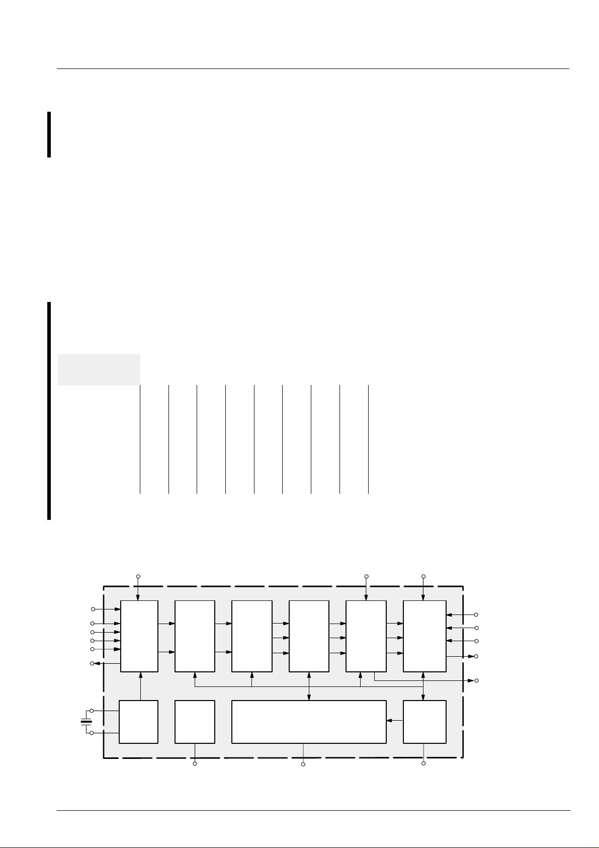
The VDP 31xxB is a Video IC family of high-quality
single-chip video processors. Modular design and a
submicron technology allow the economic integration of
features in all classes of TV sets. The VDP 31xxB family
is based on functional blocks contained in the two chips:
VDP 31xxB
Family
1H Combfilter
Horizontal Scaler
2H adapt. Comb
Color Trans. Impr.
Scan Vel. Mod.
VPC 3200A Video Processor and DDP 3300A Display
and Deflection Processor.
Each member of the family contains the entire video,
display, and deflection processing for 4:3 and 16:9
50/60 TV sets. Its performance and flexibility allow the
user to standardize his product development. Hardware
and software applications can profit from the modularity ,
as well as manufacturing, systems support, or maintenance. An overview of the VDP 31xxB video processor
family is shown in Fig. 1–1.
RGB Insertion
Prog. RGB Matrix
Tube Control
VDP 3104B
VDP 3108B
VDP 3112B
VDP 3116B
VDP 3120B
n
n
n
n
n
nn
n
n
Fig. 1–1: VDP 31xxB family overview
VRT
CIN
VIN1
VIN2
VIN3
VIN4
VOUT
Analog
Frontend
AGC,
2*8bit ADC
2H
Adaptive
Combfilter
n
n
n
n
nnn
n
Color
Decoder
NTSC,
PAL,
SECAM
n
n
n
n
n
Horizontal
Scaler
Panorama
Mode
n
n
n
n
n
n
n
n
n
n
Color Bus
Display
Processor
RGB Matrix,
CLUT,
Scan Veloc.
XREF
Analog
Backend
3*10bit DAC,
Tube Control,
RGB Switch
RGB/FB IN1
RGB/FB IN2
Half Contrast
RGB OUT
SVM
20.25
MHz
Clock Gen.
DCO
2
C
I
2
C
I
Fig. 1–2: Block diagram of the VDP 3120B
Sync & Deflection
H/V/EW
Measurement
ADC
Sense
5Micronas
Page 6
VDP 31xxB PRELIMINARY DATA SHEET
1.1. VDP Applications
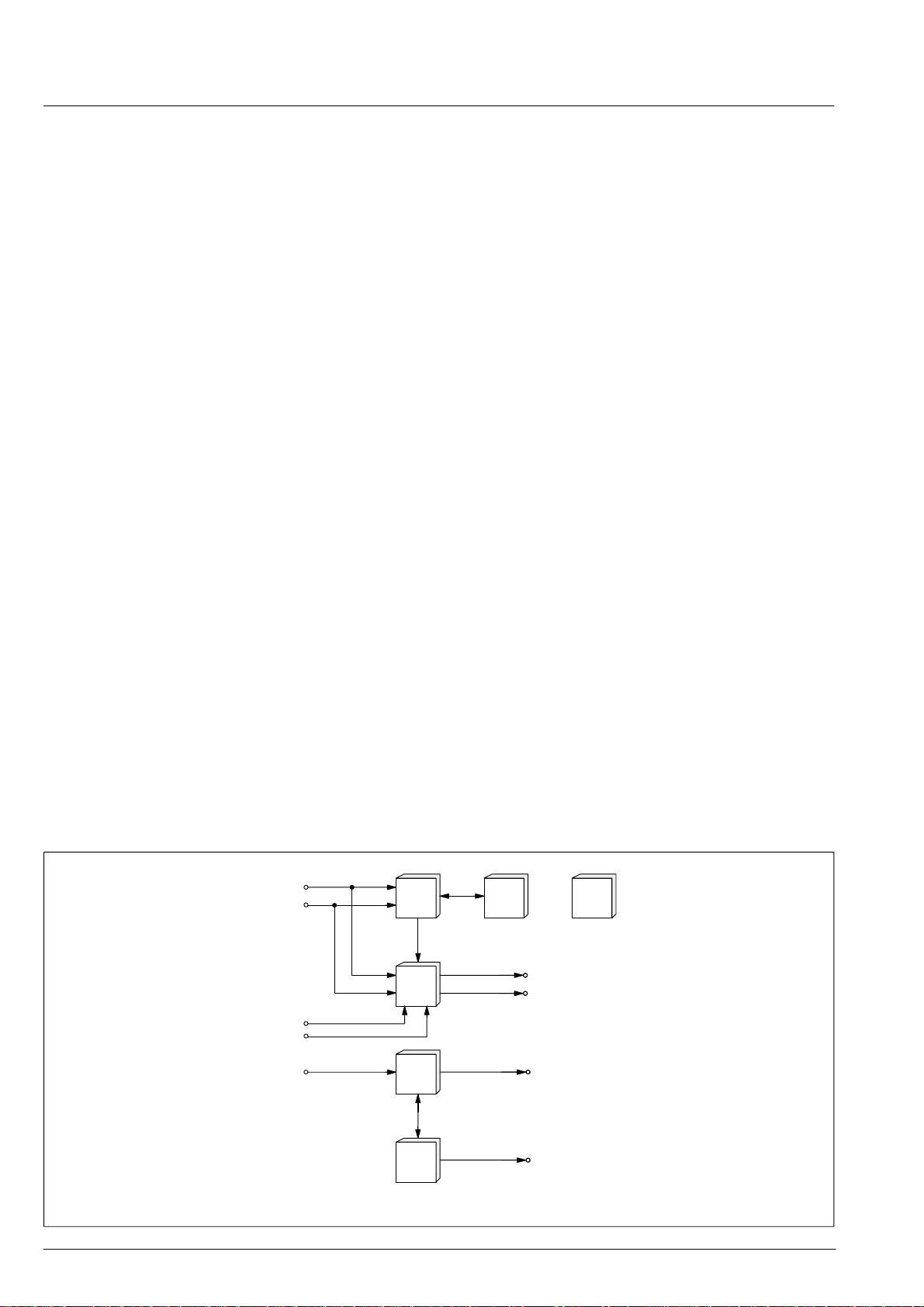
As a member of the VDP 31xxB family , the VDP 3120B
offers all video features necessary to design a state-ofthe-art TV set:
Video Decoding
– 4 composite inputs, 1 S-VHS input
– composite video & sync output
– integrated high-quality A/D converters
– adaptive 2H comb filter Y/C separator
– 1H NTSC comb filter
– multistandard color decoder (1 crystal)
– multistandard sync decoder
– black line detector
Video Processing
– horizontal scaling (0.25 to 4)
– panorama vision
– black level expander
– dynamic peaking
– soft limiter (gamma correction)
RGB Processing
– programmable RGB matrix
– digital color bus interface
– additional analog RGB / fast blank input
– half-contrast switch
– picture frame generator
Deflection
– scan velocity modulation output
– high-performance H/V deflection
– separate ADC for tube measurements
– EHT compensation
Miscellaneous
– one 20.25 MHz crystal, few external components
– embedded RISC controller (80 MIPS)
2
C-Bus Interface
– I
– single 5 V power supply
– submicron CMOS technology
– color transient improvement
Video 1
Video 2
RGB 1
RGB 2
Audio
TPU
3040
VDP
3120B
MSP
3410
– 64-pin PSDIP package
DRAM
CCU
300x
RGB
H/VDefl.
3 x Stereo
DPL
3420
Dolby Surround
Fig. 1–3: Full-feature TV set with VDP 3120B
6 Micronas
Page 7
PRELIMINARY DATA SHEET VDP 31xxB
2. Functional Description
2.1. Analog Front-End
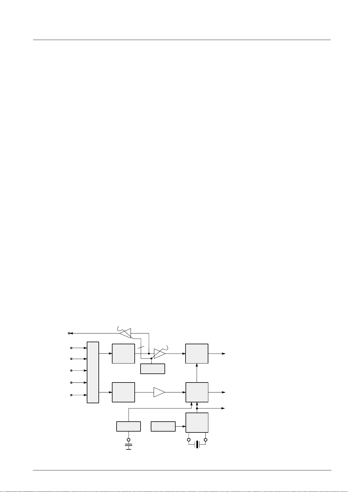
This block provides the analog interfaces to all video inputs and mainly carries out analog-to digital conversion
for the following digital video processing. A block diagram is given in Fig. 2–1.
Most of the functional blocks in the front-end are digitally
controlled (clamping, AGC, and clock-DCO). The control loops are closed by the Fast Processor (‘FP’) embedded in the decoder.
2.1.1. Input Selector
Up to five analog inputs can be connected. Four inputs
are for input of composite video or S-VHS luma signal.
These inputs are clamped to the sync back porch and
are amplified by a variable gain amplifier. One input is
for connection of S-VHS carrier-chrominance signal.
This input is internally biased and has a fixed gain amplifier.
2.1.3. Automatic Gain Control
A digitally working automatic gain control adjusts the
magnitude of the selected baseband by +6/–4.5 dB in 64
logarithmic steps to the optimal range of the ADC. The
gain of the video input stage including the ADC is 213
steps/V with the AGC set to 0 dB.
2.1.4. Analog-to-Digital Converters
Two ADCs are provided to digitize the input signals.
Each converter runs with 20.25 MHz and has 8 bit resolution. An integrated bandgap circuit generates the required reference voltages for the converters.
2.1.5. ADC Range
The ADC input range for the various input signals and
the digital representation is given in Table 2–1 and Fig.
2–2. The corresponding output signal levels of the
VDP 31xxB are also shown.
2.1.6. Digitally Controlled Clock Oscillator
2.1.2. Clamping
The composite video input signals are AC coupled to the
IC. The clamping voltage is stored on the coupling capacitors and is generated by digitally controlled current
sources. The clamping level is the back porch of the video signal. S-VHS chroma is also AC coupled. The input
pin is internally biased to the center of the ADC input
range.
Analog Video
Output
CVBS/Y
CVBS/Y
CVBS/Y
CVBS/Y/C
Chroma
VIN4
VIN3
VIN2
mux
VIN1
CIN digital Chroma
input
clamp
bias
3
gain
AGC
+6/–4.5 dB
The clock generation is also a part of the analog front
end. The crystal oscillator is controlled digitally by the
control processor; the clock frequency can be adjusted
within ±150 ppm.
2.1.7. Analog Video Output
The input signal of the Luma ADC is available at the analog video output pin. The signal at this pin must be buffered by a source follower. The output voltage is 2 V , thus
the signal can be used to drive a 75 W line. The magnitude is adjusted with an AGC in 8 steps together with the
main AGC.
ADC
ADC
digital CVBS or Luma
Fig. 2–1: Analog front-end
reference
generation
frequency
system clocks
DVCO
±150
ppm
20.25 MHz
7Micronas
Page 8
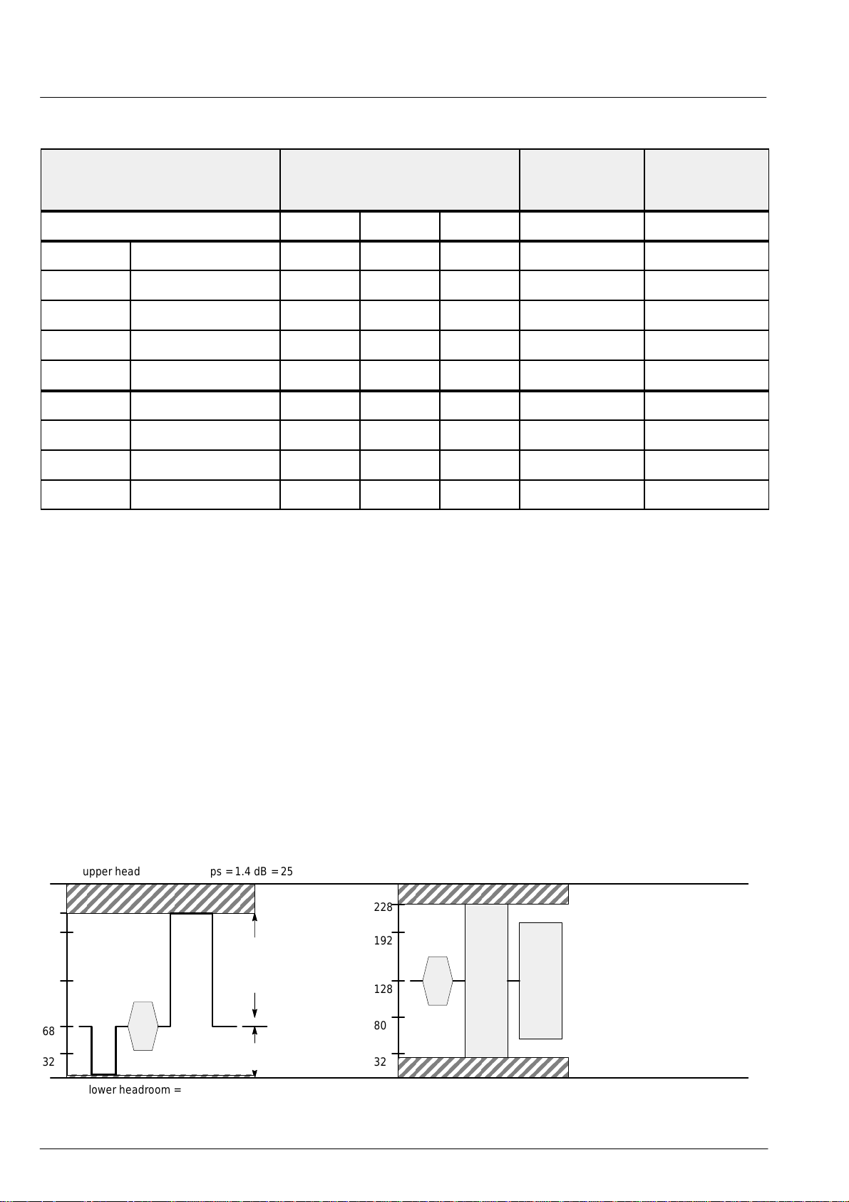
VDP 31xxB PRELIMINARY DATA SHEET
Table 2–1: ADC input range for PAL input signal and corresponding signal ranges
Signal Input Level [mVpp] ADC
Range
YCrC
b
Internal
Range
–6 dB 0 dB +4.5 dB [steps] [steps]
CVBS 100% CVBS 667 1333 2238 252 –
75% CVBS 500 1000 1679 213 –
video (luma) 350 700 1175 149 224
sync height 150 300 504 64 –
clamp level 68 16
Chroma burst 300 64 –
100% Chroma 890 190 128±112
75% Chroma 670 143 128±84
bias level 128 128
CVBS/Y Chroma
upper headroom = 38 steps = 1.4 dB = 25 IRE
255
217
192
128
68
32
0
lower headroom = 4 steps = 0.2 dB
white
black
= clamp
level
video = 100 IRE
sync = 41 IRE
headroom = 56 steps = 2.1 dB
228
100% Chroma
192
burst
128
80
32
75% Chroma
Fig. 2–2: ADC ranges for CVBS/Luma and Chroma, PAL input signal
8 Micronas
Page 9
PRELIMINARY DATA SHEET VDP 31xxB
2.2. Adaptive Comb Filter
The adaptive comb filter is used for high-quality luminance/chrominance separation for PAL or NTSC signals. The comb filter improves the luminance resolution
(bandwidth) and reduces interferences like cross-luminance and cross-color artifacts. The adaptive algorithm
can eliminate most of the mentioned errors without
introducing new artifacts or noise.
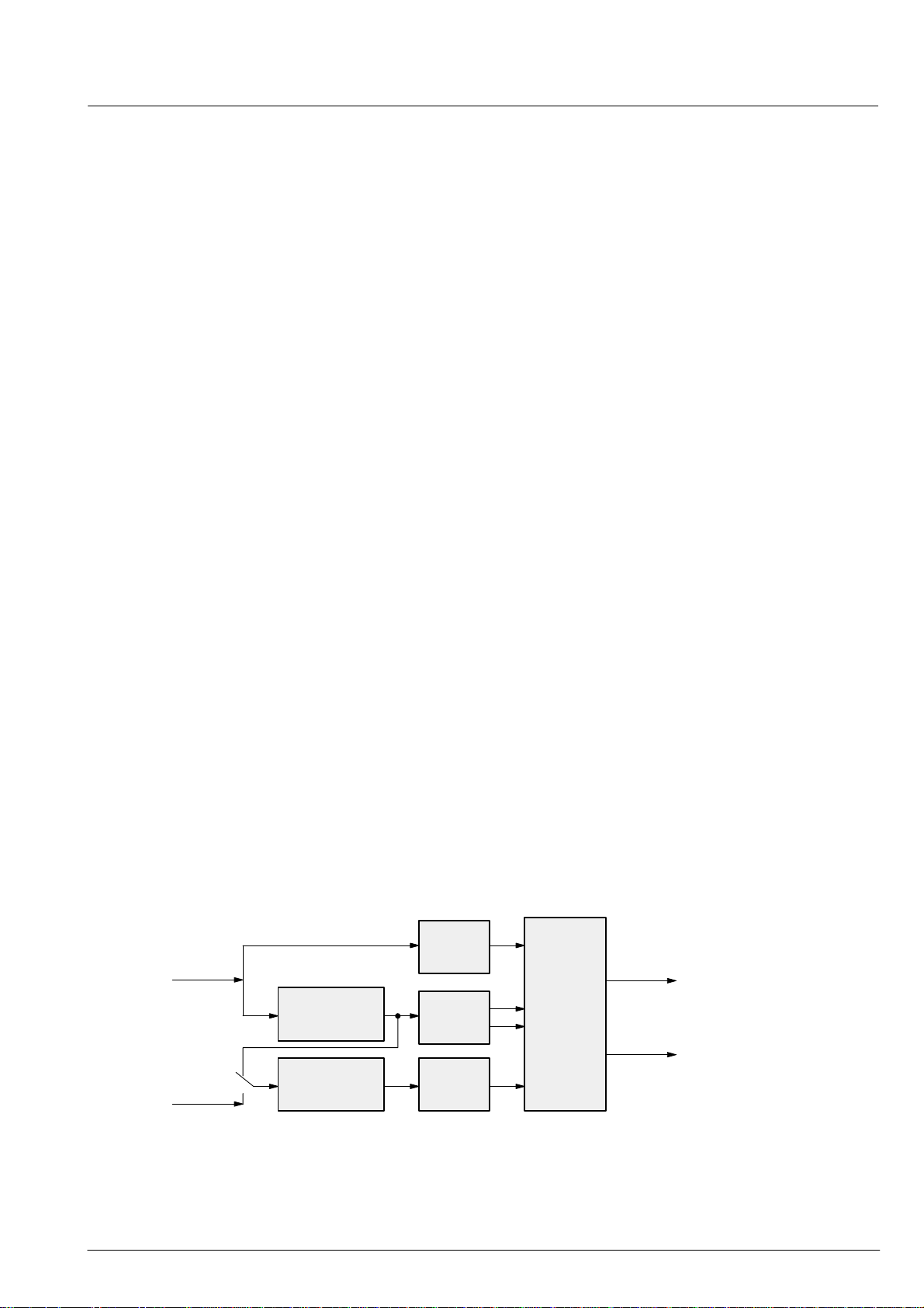
A block diagram of the comb filter is shown in Fig. 2–3.
The filter uses two line delays to process the information
of three adjacent video lines. T o have a fixed phase relationship of the color subcarrier in the three channels, the
system clock (20.25 MHz) is fractionally locked to the
color subcarrier. This allows the processing of all color
standards and substandards using a single crystal frequency.
The CVBS signal in the three channels is filtered at the
subcarrier frequency by a set of bandpass/notch filters.
The output of the three channels is used by the adaption
logic to select the weighting that is used to reconstruct
the luminance/chrominance signal from the 4 bandpass/
notch filter signals. By using soft mixing of the 4 signals
switching artifacts of the adaption algorithm are completely suppressed.
The comb filter uses the middle line as reference, therefore, the comb filter delay is one line. If the comb filter is
switched off, the delay lines are used to pass the luma/
chroma signals from the A/D converters to the luma/
chroma outputs. Thus, the comb filter delay is always
one line.
Various parameters of the comb filter are adjustable,
hence giving to the user the ability to adjust his own desired picture quality.
Two parameters (KY, KC) set the global gain of luma and
chroma comb separately; these values directly weigh
the adaption algorithm output. In this way, it is possible
to obtain a luma/chroma separation ranging from standard notch/bandpass to full comb decoding.
The parameter KB allows to choose between the two
proposed comb booster modes. This so-called feature
widely improves vertical high to low frequency transitions areas, the typical example being a multiburst to dc
change. For KB=0, this improvement is kept moderate,
whereas, in case of KB=1, it is maximum, but the risk to
increase the “hanging dots” amount for some given color
transitions is higher.
Using the default setting, the comb filter has separate
luma and chroma decision algorithms; it is however possible to switch the chroma comb factor to the current
luma adaption output by setting CC to 1.
Another interesting feature is the programmable limitation of the luma comb amount; proper limitation,
associated to adequate luma peaking, gives rise to an
enhanced 2-D resolution homogeneity . This limitation is
set by the parameter CLIM, ranging from 0 (no limitation)
to 31 (max. limitation).
The DAA parameter (1:off , 0:on) is used to disable/enable a very efficient built-in “rain effect” suppressor;
many comb filters show this side effect which gives
some vertical correlation to a 2-D uniform random area,
due to the vertical filtering. This unnatural-looking phenomenon is mostly visible on tuner images, since they
are always corrupted by some noise; and this looks like
rain.
CVBS Input
1 H Line Delay
1 H Line Delay
Chroma Input
Fig. 2–3: Block diagram of the adaptive comb filter
Bandpass
Filter
Bandpass/
Notch
Filter
Bandpass
Filter
Luma / Chroma Mixers
Adaption Logic
Luma Output
Chroma Output
9Micronas
Page 10
VDP 31xxB PRELIMINARY DATA SHEET
2.3. Color Decoder
In this block, the standard luma/chroma separation and
multi-standard color demodulation is carried out. The
color demodulation uses an asynchronous clock, thus
allowing a unified architecture for all color standards.
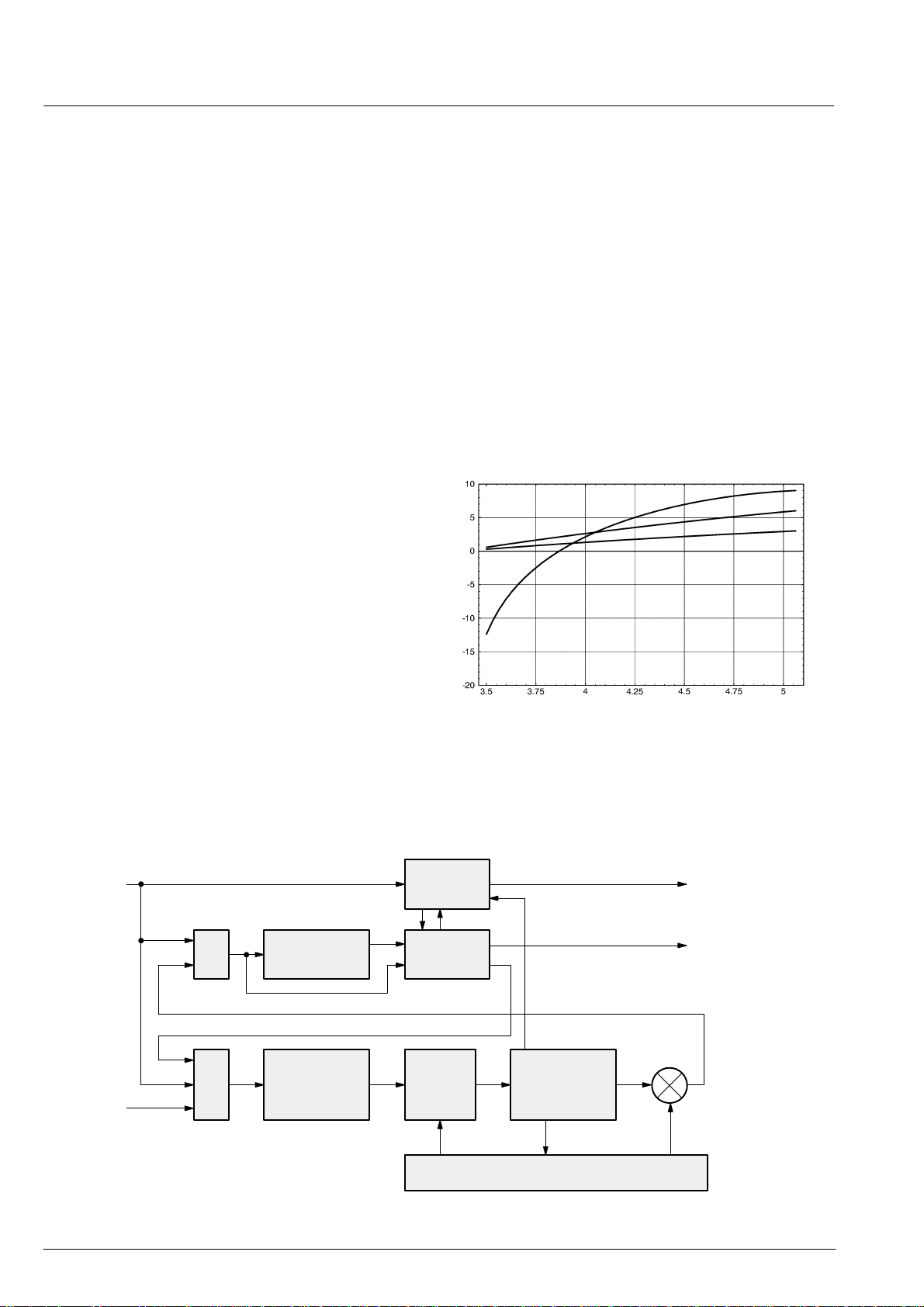
A block diagram of the color decoder is shown in Fig.
2–5. The luma as well as the chroma processing, is
shown here. The color decoder provides also some special modes, e.g. wide band chroma format which is intended for S-VHS wide bandwidth chroma.
If the adaptive comb filter is used for luma chroma separation, the color decoder uses the S-VHS mode processing. The output of the color decoder is YC
in a 4:2:2
rCb
format.
2.3.1. IF-Compensation
With off-air or mistuned reception, any attenuation at
higher frequencies or asymmetry around the color subcarrier is compensated. Four different settings of the IFcompensation are possible:
– flat (no compensation)
– 6 dB/octave
– 12 dB/octave
– 10 dB/MHz
The last setting gives a very large boost to high frequencies. It is provided for SECAM signals that are decoded
using a SAW filter specified originally for the PAL standard.
Luma / CVBS
Chroma
MUXMUX
1 H Delay
IF Compensation
DC-Reject
Fig. 2–4: Frequency response of chroma
IF-compensation
Notch
Filter
Cross-Switch
MIXER
Lowpass Filter
Phase/Freq
Demodulator
Color-PLL/Color-ACC
ACC
Luma
Chroma /CrC
b
Fig. 2–5: Color decoder
10 Micronas
Page 11
PRELIMINARY DATA SHEET VDP 31xxB
2.3.2. Demodulator
The entire signal (which might still contain luma) is now
quadrature-mixed to the baseband. The mixing frequency is equal to the subcarrier for PAL and NTSC, thus
achieving the chroma demodulation. For SECAM, the
mixing frequency is 4.286 MHz giving the quadrature
baseband components of the FM modulated chroma.
After the mixer, a lowpass filter selects the chroma components; a downsampling stage converts the color difference signals to a multiplexed half rate data stream.
The subcarrier frequency in the demodulator is generated by direct digital synthesis; therefore, substandards
such as PAL 3.58 or NTSC 4.43 can also be demodulated.
2.3.3. Chrominance Filter
The demodulation is followed by a lowpass filter for the
color difference signals for P AL/NTSC. SECAM requires
a modified lowpass function with bell-filter characteristic.
At the output of the lowpass filter, all luma information is
eliminated.
The lowpass filters are calculated in time multiplex for
the two color signals. Three bandwidth settings (narrow,
normal, broad) are available for each standard. For P AL/
NTSC, a wide band chroma filter can be selected. This
filter is intended for high bandwidth chroma signals, e.g.
a nonstandard wide bandwidth S-VHS signal.
2.3.4. Frequency Demodulator
The frequency demodulator for demodulating the SECAM signal is implemented as a CORDIC-structure. It
calculates the phase and magnitude of the quadrature
components by coordinate rotation.
The phase output of the CORDIC processor is differentiated to obtain the demodulated frequency. After the
deemphasis filter, the Dr and Db signals are scaled to
standard C
amplitudes and fed to the crossover-
rCb
switch.
2.3.5. Burst Detection
In the PAL/NTSC-system the burst is the reference for
the color signal. The phase and magnitude outputs of
the CORDIC are gated with the color key and used for
controlling the phase-lock-loop (APC) of the demodulator and the automatic color control (ACC) in P AL/NTSC.
The ACC has a control range of +30...–6 dB.
For SECAM decoding, the frequency of the burst is measured. Thus, the current chroma carrier frequency can
be identified and is used to control the SECAM processing. The burst measurements also control the color killer operation; they can be used for automatic standard
detection as well.
2.3.6. Color Killer Operation
The color killer uses the burst-phase / burst-frequency
measurement to identify a PAL/NTSC or SECAM color
signal. For PAL/NTSC, the color is switched off (killed)
as long as the color subcarrier PLL is not locked. For SECAM, the killer is controlled by the toggle of the burst frequency. The burst amplitude measurement is used to
switch-off the color if the burst amplitude is below a programmable threshold. Thus, color will be killed for very
noisy signals. The color amplitude killer has a programmable hysteresis.
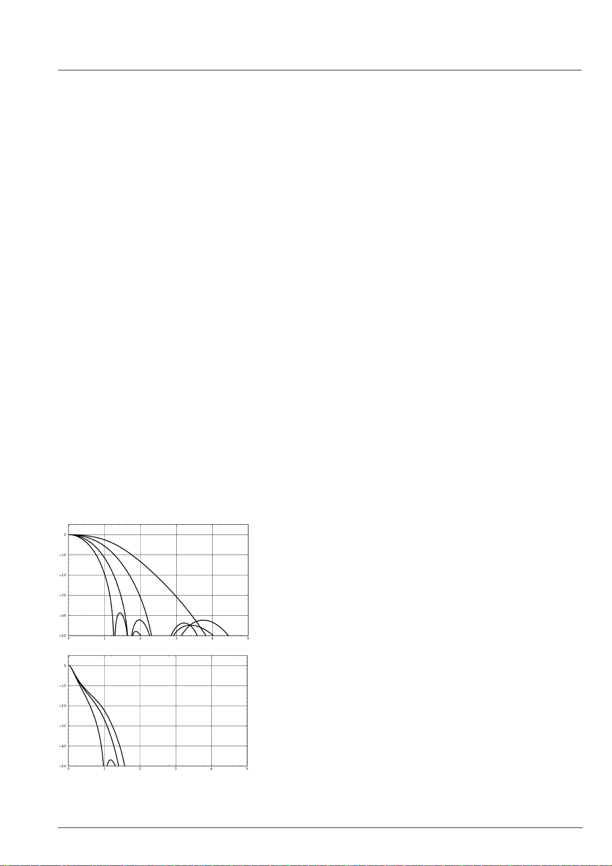
PAL/NTSC
SECAM
Fig. 2–6: Frequency response of chroma filters
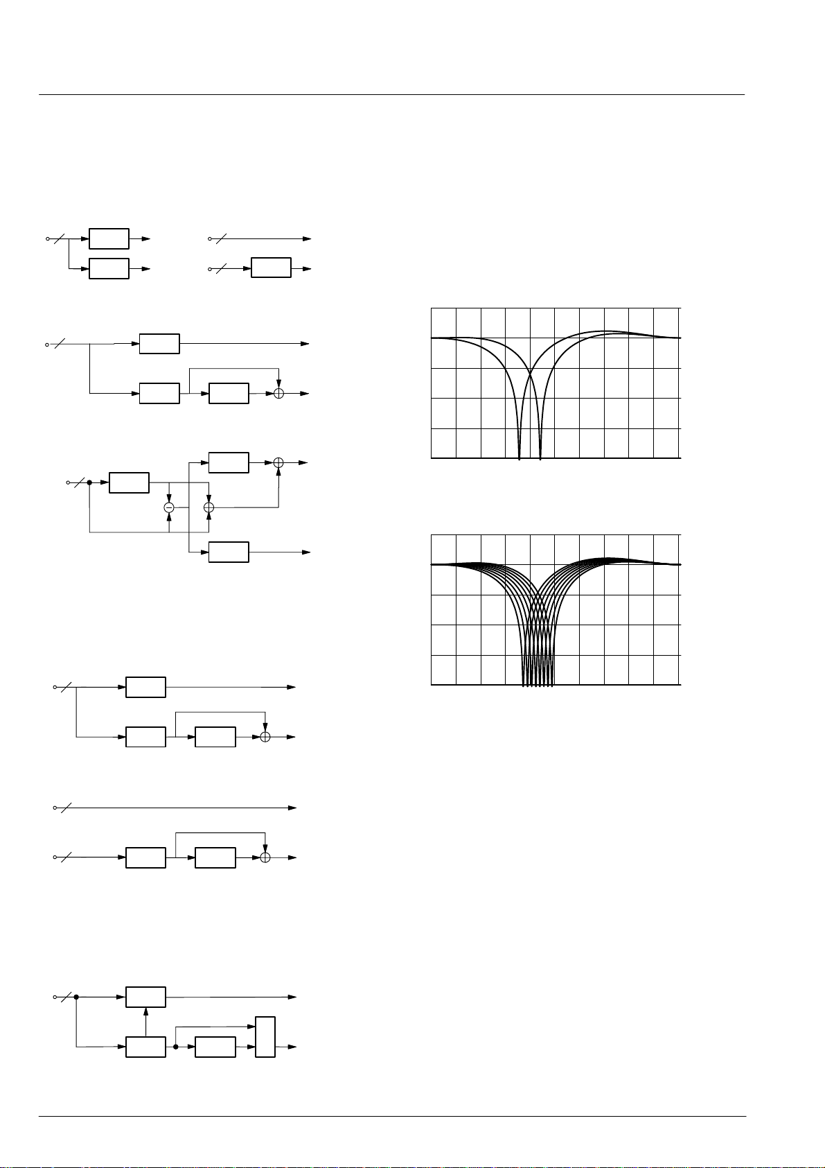
2.3.7. PAL Compensation/1-H Comb Filter
The color decoder uses one fully integrated delay line.
Only active video is stored.
The delay line application depends on the color standard:
– NTSC: 1-H comb filter or color compensation
– PAL: color compensation
– SECAM: crossover-switch
In the NTSC compensated mode, Fig. 2–7 c), the color
signal is averaged for two adjacent lines. Thus, crosscolor distortion and chroma noise is reduced. In the
NTSC combfilter mode, Fig. 2–7 d), the delay line is in
the composite signal path, thus allowing reduction of
11Micronas
Page 12
VDP 31xxB PRELIMINARY DATA SHEET
cross-color components, as well as cross-luminance.
The loss of vertical resolution in the luminance channel
is compensated by adding the vertical detail signal with
removed color information.
CVBS
8
Notch
filter
Chroma
Process.
Y
C C
r b
Luma
8
Chroma
8
Chroma
Process.
Y
C C
r b
a) conventional b) S-VHS
CVBS
8
Notch
filter
Chroma
Process.
1 H
Delay
Y
C C
r b
c) compensated
CVBS
Notch
1 H
8
Delay
filter
Y
2.3.8. Luminance Notch Filter
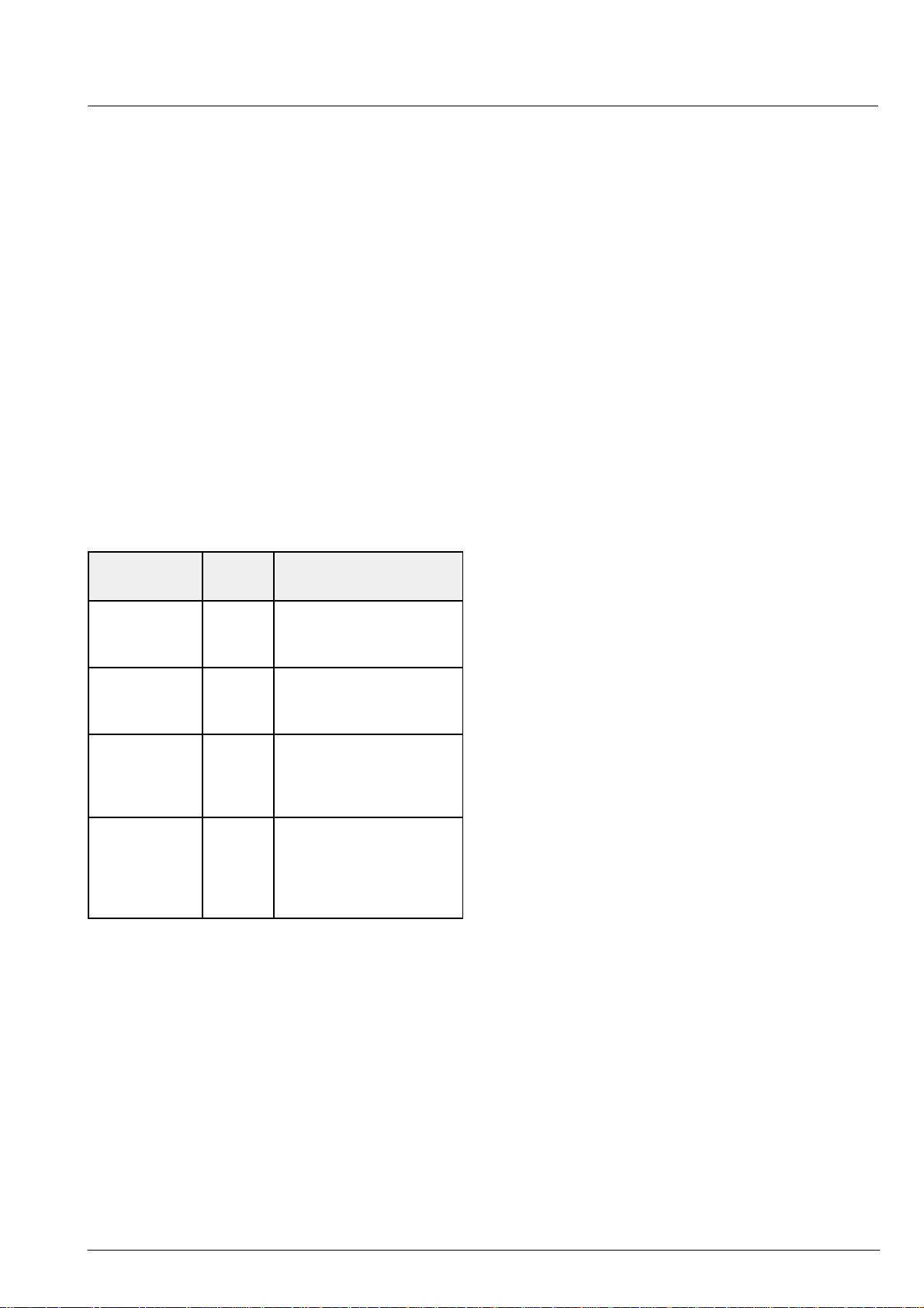
If a composite video signal is applied, the color information is suppressed by a programmable notch filter. The
position of the filter center frequency depends on the
subcarrier frequency for PAL/NTSC. For SECAM, the
notch is directly controlled by the chroma carrier frequency. This considerably reduces the cross-luminance. The frequency responses for all three systems
are shown in Fig. 2–10.
dB
10
0
–10
–20
–30
–40
024 68 10
MHz
PAL/NTSC notch filter
Chroma
Process.
d) comb filter
Fig. 2–7: NTSC color decoding options
CVBS
8
Notch
filter
Chroma
Process.
1 H
Delay
a) conventional
Luma
8
Chroma
8
Chroma
Process.
1 H
Delay
b) S-VHS
Fig. 2–8: PAL color decoding options
CVBS
8
Notch
filter
Chroma
Process.
1 H
Delay
MUX
Fig. 2–9: SECAM color decoding
C C
Y
C C
r b
Y
C C
r b
Y
C C
r b
r b
dB
10
0
–10
–20
–30
–40
024 68 10
MHz
SECAM notch filter
Fig. 2–10: Frequency responses of the luma
notch filter for PAL, NTSC, and SECAM
2.3.9. Skew Filtering
The system clock is free-running and not locked to the
TV line frequency . Therefore, the ADC sampling pattern
is not orthogonal. The decoded YC
signals are con-
rCb
verted to an orthogonal sampling raster by the skew filters, which are part of the scaler block.
The skew filters allow the application of a group delay to
the input signals without introducing waveform or frequency response distortion.
The amount of phase shift of this filter is controlled by the
horizontal PLL1. The accuracy of the filters is 1/32
clocks for luminance and 1/4 clocks for chroma. Thus
the 4:2:2 YC
data is in an orthogonal pixel format
rCb
even in the case of nonstandard input signals such as
VCR.
12 Micronas
Page 13
PRELIMINARY DATA SHEET VDP 31xxB
2.4. Horizontal Scaler
The 4:2:2 YCrCb signal from the color decoder is processed by the horizontal scaler. The scaler block allows
a linear or nonlinear horizontal scaling of the input video
signal in the range of 0.25 to 4. Nonlinear scaling, also
called “panorama vision”, provides a geometrical distor-
tion of the input picture. It is used to fit a picture with 4:3
format on a 16:9 screen by stretching the picture geometry at the borders. Also, the inverse effect can be produced by the scaler. A summary of scaler modes is given
in Table 2–2.
The scaler contains a programmable decimation filter, a
1-line FIFO memory , and a programmable interpolation
filter. The scaler input filter is also used for pixel skew
correction, see 2.3.9. The decimator/interpolator structure allows optimal use of the FIFO memory. The controlling of the scaler is done by the internal Fast Processor.
Table 2–2: Scaler modes
Mode Scale
Description
Factor
Compression
4:3 → 16:9
0.75
linear
4:3 source displayed on a
16:9 tube,
with side panels
2.5. Black-Line Detector
In case of a letterbox format input video, e.g. Cinemascope, PAL+ etc., black areas at the upper and lower
part of the picture are visible. It is suitable to remove or
reduce these areas by a vertical zoom and/or shift operation.
The VDP 31xxB supports this feature by a letterbox detector. The circuitry detects black video lines by measuring the signal amplitude during active video. For every
field the number of black lines at the upper and lower
part of the picture are measured, compared to the previous measurement and the minima are stored in the
2
I
C-register BLKLIN. T o adjust the picture amplitude, the
external controller reads this register, calculates the vertical scaling coefficient and transfers the new settings,
e.g. vertical sawtooth parameters, horizontal scaling coefficient etc., to the VDP.
Letterbox signals containing logos on the left or right
side of the black areas are processed as black lines,
while subtitles, inserted in the black areas, are processed as non-black lines. Therefore the subtitles are
visible on the screen. T o suppress the subtitles, the vertical zoom coefficient is calculated by selecting the larger
number of black lines only . Dark video scenes with a low
contrast level compared to the letterbox area are indicated by the BLKPIC bit.
Panorama
4:3 → 16:9
Zoom
4:3 → 4:3
Panorama
4:3 → 4:3
nonlinear
compr
1.33
linear
nonlinear
zoom
4:3 source displayed on a
16:9 tube,
Borders distorted
Letterbox source (PAL+)
displayed on a 4:3 tube,
vertical overscan with
cropping of side panels
Letterbox source (PAL+)
displayed on a 4:3 tube,
vertical overscan, borders distorted, no cropping
2.6. Test Pattern Generator
The YCrCb outputs of the front-end can be switched to
a test mode where YCrCb data are generated digitally
in the VDP 31xxB. Test patterns include luma/chroma
ramps, flat fields and a pseudo color bar pattern.
13Micronas
Page 14
VDP 31xxB PRELIMINARY DATA SHEET
2.7. Video Sync Processing
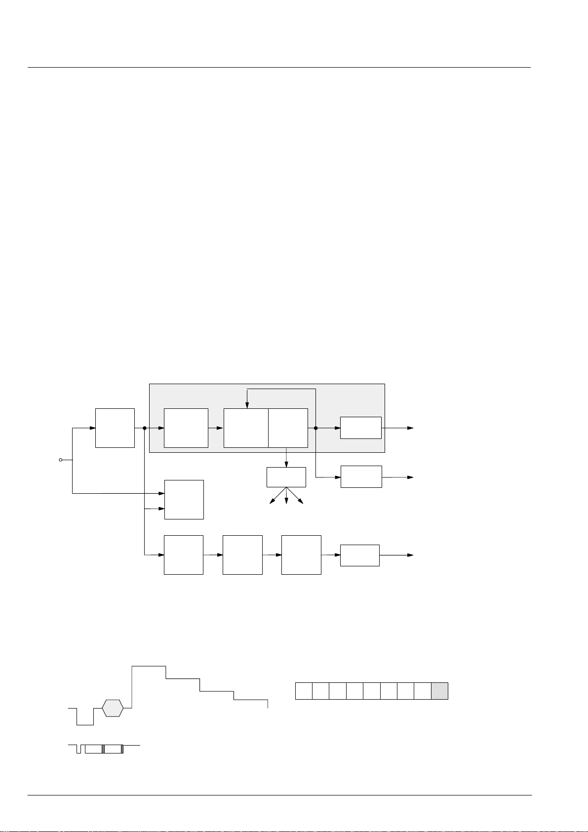
Fig. 2–11 shows a block diagram of the front-end sync
processing. To extract the sync information from the
video signal, a linear phase lowpass filter eliminates all
noise and video contents above 1 MHz. The sync is separated by a slicer; the sync phase is measured. A variable window can be selected to improve the noise immunity of the slicer. The phase comparator measures the
falling edge of sync, as well as the integrated sync pulse.
The sync phase error is filtered by a phase-locked loop
that is computed by the FP. All timing in the front-end is
derived from a counter that is part of this PLL, and it thus
counts synchronously to the video signal.
A separate hardware block measures the signal back
porch and also allows gathering the maximum/minimum
of the video signal. This information is processed by the
FP and used for gain control and clamping.
For vertical sync separation, the sliced video signal is integrated. The FP uses the integrator value to derive vertical sync and field information.
The information extracted by the video sync processing
is multiplexed onto the hardware front sync signal (FSY)
and is distributed to the rest of the video processing system. The format of the front sync signal is given in
Fig. 2–12.
The data for the vertical deflection, the sawtooth, and the
East-West correction signal is calculated by the
VDP 31xxB. The data is buffered in a FIFO and transferred to the back-end by a single wire interface.
Frequency and phase characteristics of the analog video signal are derived from PLL1. The results are fed to
the scaler unit for data interpolation and orthogonalization and to the clock synthesizer for line-locked clock
generation. Horizontal and vertical syncs are latched
with the line-locked clock.
video
input
lowpass
1 MHz
&
syncslicer
horizontal
sync
separation
clamp &
signal
meas.
vertical
sync
separation
Fig. 2–11: Sync separation block diagram
phase
comparator
&
lowpass
clamping, colorkey, FIFO_write
Sawtooth
Parabola
Calculation
counter
front-end
timing
FIFO
PLL1
generator
synthesizer
front
sync
clock
syncs
vertical
serial
data
front sync
skew
vblank
field
clock
H/V syncs
vertical
E/W
sawtooth
input
analog
video
FSY
skew skew
F1
LSB
F0 reserved
(not in scale)
F1
F0
MSB
not
used
FV
Parity
V: vertical sync
0 = off
1 = on
F: field #
0 = field 1
1 = field 2
Fig. 2–12: Front sync format
14 Micronas
Page 15
PRELIMINARY DATA SHEET VDP 31xxB
2.8. Display Part
In the display part the conversion from digital YCrCb to
analog RGB is carried out. A block diagram is shown in
Figure 2–20. In the luminance processing path, contrast
and brightness adjustments and a variety of features,
such as black level expansion, dynamic peaking and
soft limiting, are provided. In the chrominance path, the
C
signals are converted to 20.25 MHz sampling rate
rCb
and filtered by a color transient improvement circuit. The
YC
signals are converted by a programmable matrix
rCb
to RGB color space.
The display processor provides separate control settings for two pictures, i.e. different coefficients for a
‘main’ and a ‘side’ picture.
The digital OSD insertion circuit allows the insertion of
a 5-bit OSD signal. The color space for this signal is controlled by a partially programmable color look-up table
(CLUT) and contrast adjustment.
The OSD signals and the display clock are synchronized
to the horizontal flyback. For the display clock, a gate
delay phase shifter is used. In the analog backend, three
10-bit digital-to-analog converters provide the analog
output signals.
2.8.1. Luma Contrast Adjustment
The contrast of the luminance signal can be adjusted by
multiplication with a 6-bit contrast value. The contrast
value corresponds to a gain factor from 0 to 2, where the
value 32 is equivalent to a gain of 1. The contrast can be
adjusted separately for main picture and side picture.
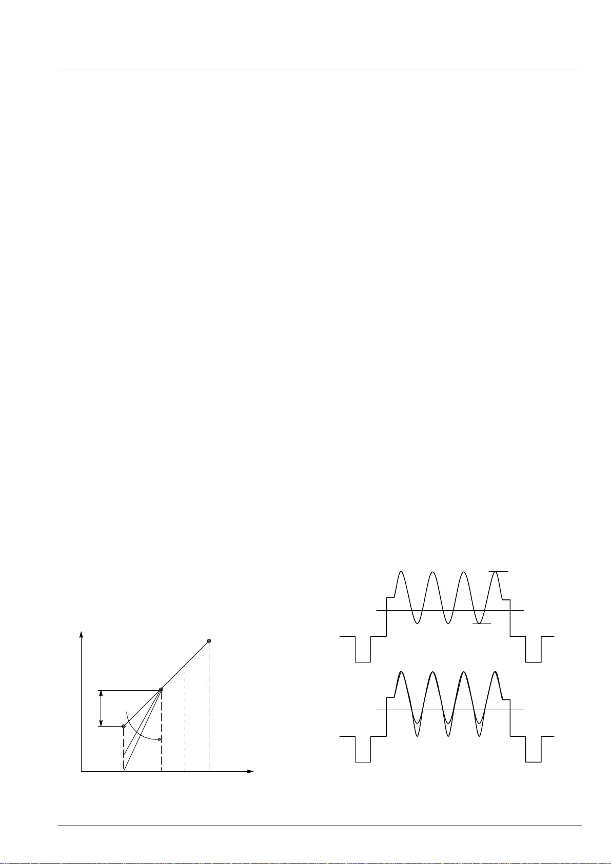
2.8.2. Black Level Expander
The black level expander enhances the contrast of the
picture. Therefore the luminance signal is modified with
an adjustable, non-linear function. Dark areas of the picture are changed to black, while bright areas remain unchanged. The advantage of this black level expander is
that the black expansion is performed only if it will be
most noticeable to the viewer.
The black level expander works adaptively. Depending
on the measured amplitudes ‘L
min
’ and ‘L
’ of the low-
max
pass-filtered luminance and an adjustable coefficient
BTLT, a tilt point ‘L
= L
L
t
’ is established by
t
+ BTLT (L
min
max
– L
min
).
Above this value there is no expansion, while all luminance values below this point are expanded according
to:
L
= Lin + BAM (Lin – Lt)
out
A second threshold, L
, can be programmed, above
tr
which there is no expansion. The characteristics of the
black level expander are shown in Fig. 2–13 and Fig.
2–14.
The tilt point L
is a function of the dynamic range of the
t
video signal. Thus, the black level expansion is only performed when the video signal has a large dynamic
range. Otherwise, the expansion to black is zero. This allows the correction of the characteristics of the picture
tube.
L
out
L
t
BAM
BTLT
L
min
L
tr
L
L
tr
BTHR
max
L
in
Fig. 2–13: Characteristics of the black level expander
a)
b)
Fig. 2–14: Black-level-expansion
a) luminance input
b) luminance input and output
L
max
L
t
L
min
L
t
15Micronas
Page 16
PRELIMINARY DATA SHEETVDP 31xxB
2.8.3. Dynamic Peaking
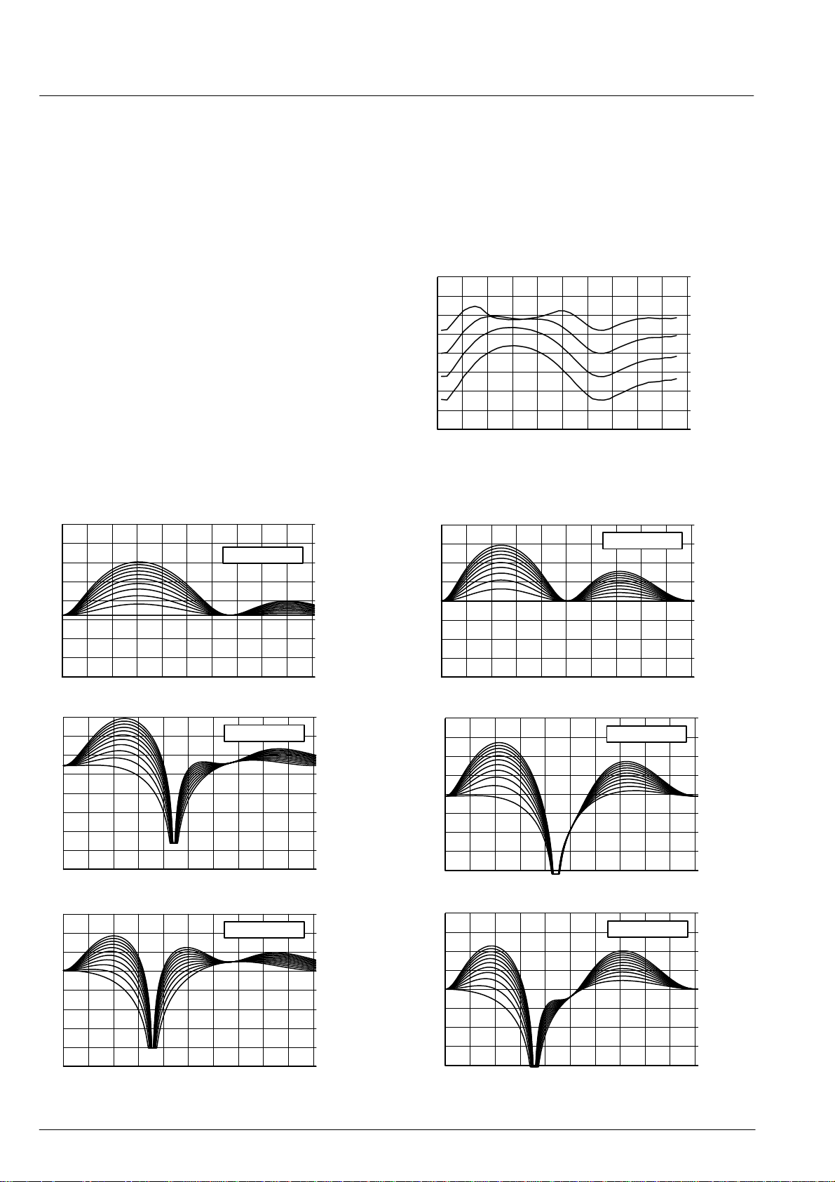
Especially with decoded composite signals and notch filter luminance separation, as input signals, it is necessary to improve the luminance frequency characteristics. With transparent, high-bandwidth signals, it is
sometimes desirable to soften the image.
In the VDP 31xxB, the luma response is improved by ‘dy-
namic’ peaking. The algorithm has been optimized regarding step and frequency response. It adapts to the
amplitude of the high frequency part. Small AC amplitudes are processed, while large AC amplitudes stay
nearly unmodified.
The dynamic range can be adjusted from *14 to
)14 dB for small high frequency signals. There is separate adjustment for signal overshoot and for signal undershoot. For large signals, the dynamic range is limited
by a non-linear function that does not create any visible
alias components. The peaking can be switched over to
“softening” by inverting the peaking term by software.
dB
20
15
10
5
0
–5
–10
–15
–20
024 68 10
CF= 3.2 MHz
S-VHS
MHz
The center frequency of the peaking filter is switchable
from 2.5 MHz to 3.2 MHz. For S-VHS and for notch filter
color decoding, the total system frequency responses
for both PAL and NTSC are shown in figure 2–16.
Transients, produced by the dynamic peaking when
switching video source signals, can be suppressed via
the priority bus.
dB
20
15
10
5
0
–5
–10
–15
–20
024 68 10
MHz
Fig. 2–15: Dynamic peaking frequency response
dB
20
15
10
5
0
–5
–10
–15
–20
024 68 10
CF= 2.5 MHz
MHz
dB
20
15
10
5
0
–5
–10
–15
–20
024 68 10
dB
20
15
10
5
0
–5
–10
–15
–20
024 68 10
CF= 3.2 MHz
CF= 3.2 MHz
PAL/SECAM
MHz
NTSC
MHz
dB
20
15
10
5
0
–5
–10
–15
–20
024 68 10
dB
20
15
10
5
0
–5
–10
–15
–20
024 68 10
Fig. 2–16: Total frequency response for peaking filter and S-VHS, PAL, NTSC
CF= 2.5 MHz
MHz
CF= 2.5 MHz
MHz
16 Micronas
Page 17
PRELIMINARY DATA SHEET VDP 31xxB
2.8.4. Digital Brightness Adjustment
The DC-level of the luminance signal can be adjusted by
adding an 8-bit number in the luminance signal path in
front of the softlimiter.
With a contrast adjustment of 32 (gain+1) the signal can
be shifted by "100%. After the brightness addition, the
negative going signals are limited to zero. It is desirable
to keep a small positive offset with the signal to prevent
undershoots produced by the peaking from being cut.
The digital brightness adjustment is separate for main
and side picture.
2.8.5. Soft Limiter
The dynamic range of the processed luma signal must
be limited to prevent the CRT from overload. An appropriate headroom for contrast, peaking and brightness
can be adjusted by the TV manufacturer according to the
CRT characteristics. All signals above this limit will be
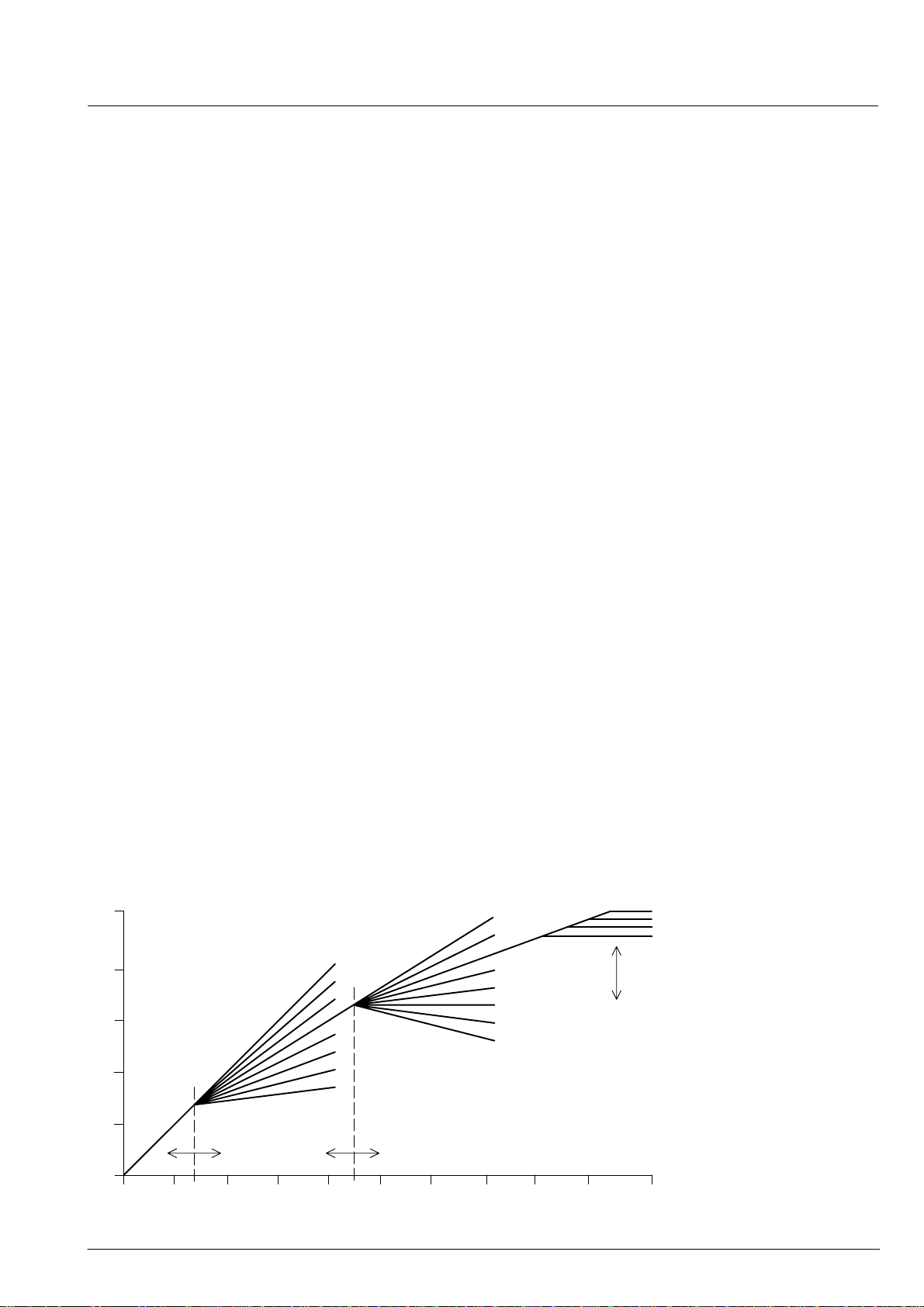
‘soft’-clipped. A characteristic diagram of the soft limiter
is shown in Fig. 2–17. The total limiter consists of three
parts:
Part 1 includes adjustable tilt point and gain. The gain
before the tilt value is 1. Above the tilt value, a part
(0...15/16) of the input signal is subtracted from the input
signal itself. Therefore, the gain is adjustable from 16/16
to 1/16, when the slope value varies from 0 to 15. The
tilt value can be adjusted from 0 to 511.
Part 2 has the same characteristics as part 1. The subtracting part is also relative to the input signal, so the
total differential gain will become negative if the sum of
slope 1 and slope 2 is greater than 16 and the input signal is above the both tilt values (see characteristics).
Finally , the output signal of the soft limiter will be clipped
by a hard limiter adjustable from 256 to 511.
2.8.6. Chroma Input
The chroma input signal is a multiplexed C
and CB sig-
R
nal in 8-bit binary offset code. It can be switched between normal and inverted signal and between two’s
complement and binary offset code. The delay in respect to the luminance input can be adjusted in 5 steps
within a range of "2 clock periods.
2.8.7. Chroma Interpolation
A linear phase interpolator is used to convert the chroma
sampling rate from 10.125 MHz (4:2:2) to 20.25 MHz
(4:4:4). All further processing is carried out at the full
sampling rate.
511
400
300
200
100
0
Output
0
tilt 1 [ 0...511]
100 200 300
Part 1 Part 2 Hard limiter
0
slope 1 [0...15]
0
2
4
6
8
10
12
14
tilt 2 [0...511]
400 500
600 700 800
2
4
6
8
10
12
14
slope 2 [0...15]
Fig. 2–17: Characteristic of soft limiter a and b and hard limiter
range= 256...511
900
1023
Calculation Example for the
Softlimiter Input Amplitude.
(The real signal processing in
the limiter is 2 bit more than
described here)
Y Input 16...235 (ITUR)
Black Level 16 (constant)
Contrast 63
Dig. Brightness 20
BLE off
Peaking off
Limiter input signal:
(Yin-Black Level)·Contr ./32 + Brightn.
(235–16) · 63/32 + 20 = 451
Limiter Input
17Micronas
Page 18
PRELIMINARY DATA SHEETVDP 31xxB
2.8.8. Chroma Transient Improvement
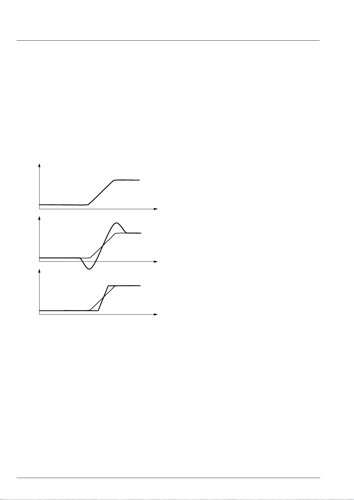
The intention of this block is to enhance the chroma
resolution. A correction signal is calculated by differentiation of the color difference signals. The differentiation
can be selected according to the signal bandwidth, e.g.
for PAL/NTSC/SECAM or digital component signals,
respectively. The amplitude of the correction signal is
adjustable. Small noise amplitudes in the correction signal are suppressed by an adjustable coring circuit. To
eliminate ‘wrong colors’, which are caused by over and
undershoots at the chroma transition, the sharpened
chroma signals are limited to a proper value automatically.
a)
Cr in
Cb in
t
b)
Ampl.
t
2.8.9. Inverse Matrix
A 6-multiplier matrix transcodes the Cr and Cb signals
to R–Y, B–Y, and G–Y. The multipliers are also used to
adjust color saturation in the range of 0 to 2. The coefficients are signed and have a resolution of 9 bits. There
are separate matrix coefficients for main and side pictures. The matrix computes:
R–Y+MR1*Cb)MR2*Cr
G–Y+MG1*Cb)MG2*Cr
B–Y+MB1*Cb)MB2*Cr
The initialization values for the matrix are computed
from the standard ITUR (CCIR) matrix:
Ǔ
Y
Cb
Cr
1
1
* 0.345
1
0
1.773
R
G
+
ǒ
B
For a contrast setting of CTM+32, the matrix values are
scaled by a factor of 64, see also table 3–1.
2.8.10. RGB Processing
After adding the post-processed luma, the digital RGB
signals are limited to 10 bits. Three multipliers are used
to digitally adjust the white drive. Using the same multipliers an average beam current limiter is implemented.
See also section 2.9.1. ‘CRT Measurement and Con-
trol’.
1.402
* 0.713
0
c)
Cr out
Cb out
a) Cr Cb input of DTI
b) Cr Cb input)Correction signal
c) sharpened and limited Cr Cb
Fig. 2–18: Digital Color Transient Improvement
2.8.11. OSD Color Lookup Table
The VDP 31xxB has five input lines for an OSD signal.
This signal forms a 5-bit address for a color look-up table
t
(CLUT). The CLUT is a memory with 32 words where
each word holds a RGB value.
Bits 0 to 3 (bit 4+0) form the addresses for the ROM part
of the OSD, which generates full RGB signals (bit 0 to 2)
and half-contrast RGB signals (bit 3).
Bit 4 addresses the RAM part of the OSD with 16 freely
programmable colors, addressable with bit 0 to 3. The
programming is done via the I
The amplitude of the CLUT output signals can be adjusted separately for R, G and B via the I2C-bus. The
switchover between video RGB and OSD RGB is done
via the Priority bus.
2
C-bus.
18 Micronas
Page 19
PRELIMINARY DATA SHEET VDP 31xxB
2.8.12. Picture Frame Generator
When the picture does not fill the total screen (height or
width too small) it is surrounded with black areas. These
areas (and more) can be colored with the picture frame
generator. This is done by switching over the RGB signal
from the matrix to the signal from the OSD color look-up
table.
The width of each area (left, right, upper, lower) can be
adjusted separately. The generator starts on the right,
respectively lower side of the screen and stops on the
left, respectively upper side of the screen. This means,
it runs during horizontal, respectively vertical flyback.
The color of the complete border can be stored in the
programmable OSD color look-up table in a separate
address. The format is 3 4 bit RGB. The contrast can
be adjusted separately.
The picture frame generator includes a priority master
circuit. Its priority is programmable and the border is
generated only if the priority is higher than the priority at
the PRIO bus. Therefore the border can be underlay or
overlay depending on the picture source.
2.8.13. Priority Codec
2.8.14. Scan Velocity Modulation
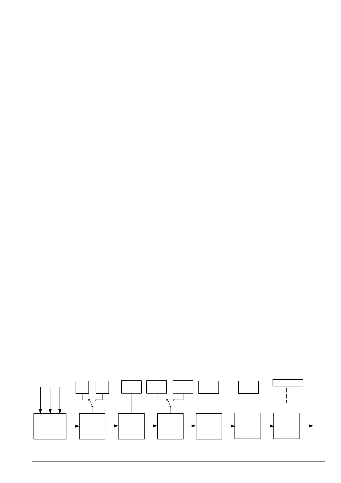
The RGB input signal of the SVM is converted to Y in a
simple matrix. Then the Y signal is differentiated by a filter of the transfer function 1–Z
–N
, where N is programmable from 1 to 6. With a coring, some noise can be suppressed. This is followed by a gain adjustment and an
adjustable limiter. The analog output signal is generated
by an 8-bit D/A converter.
The signal delay can be adjusted by ±3.5 clocks in halfclock steps. For the gain and filter adjustment there are
two parameter sets. The switching between these two
sets is done with the same RGB switch signal that is
used for switching between video-RGB and OSD-RGB
for the RGB outputs. (See Fig. 2–19).
2.8.15. Display Phase Shifter
A phase shifter is used to partially compensate the
phase differences between the video source and the flyback signal. By using the described clock system, this
phase shifter works with an accuracy of approximately
1 ns. It has a range of 1 clock period which is equivalent
to ±24.7 ns at 20.25 MHz. The large amount of phase
shift (full clock periods) is realized in the front-end circuit.
The priority decoder has three input lines for up to eight
priorities. The highest priority is all three lines at low level. A 5-bit information is attached to each priority (see
table 3–1 ‘Priority Bus’). These bits are programmable
via the I
2
C-bus and have the following meanings:
– one of two contrast, brightness and matrix values for
main and side picture
– RGB from video signal or color look-up table
– disable/enable black level expander
– disable/enable peaking transient suppression when
signal is switched
– disable/enable analog fast blank input 1
– disable/enable analog fast blank input 2
GRB
N1 N2
Coring
Gain1 Gain2
Limit
Delay
RGB Switch
Matrix and
Shaping
Modulation
Notch
Differentiator
–Nx
1–Z
Fig. 2–19: SVM block diagram
Coring
adjustment
Gain
adjustment
Limiter
Delay
adjustment
D/A
Converter
Output
19Micronas
Page 20
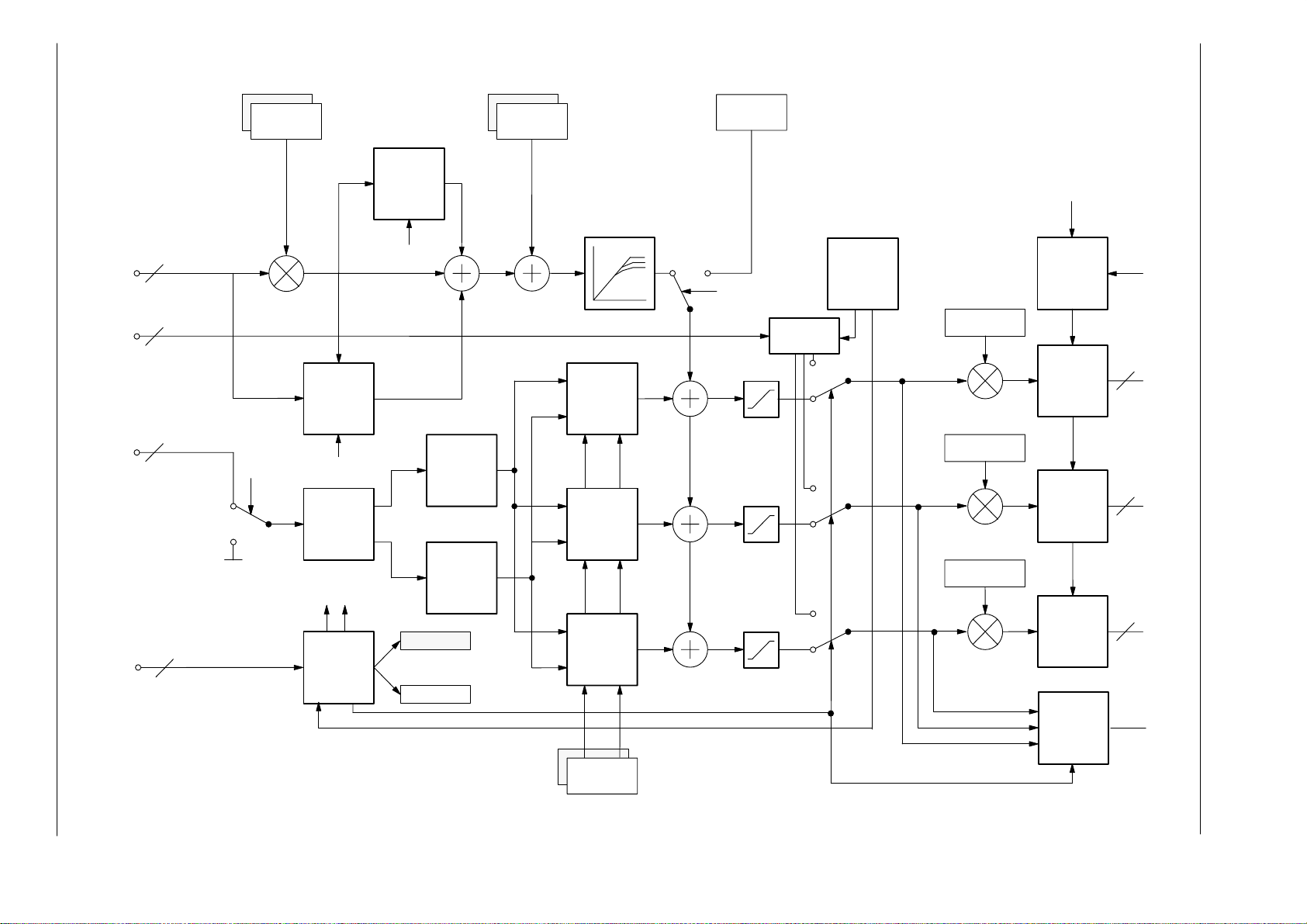
20 Micronas
Fig. 2–20: Digital back-end
dig.
Y in
8
5
dig. OSD in
8
dig.
CrCb in
contrast
expander
blanking
for CRTmeasurement
black
level
prio
Interpol
4:4:4
dynamic
peaking
prio
Cr
DTI
(Cr)
brightness
+ offset
softlimiter
Matrix
R’
Matrix
G’
whitedrive
measurement
luma insert
for CRTmeasurement
Y
R
G
CLUT,
Contrast
Picture
Frame
Generator
whitedrive R
x beamcurr. lim.
whitedrive G
x beamcurr. lim.
clock
display
& clock
control
Phase
Shift
0...1 clock
Phase
Shift
0...1 clock
horizontal
flyback
dig.
Rout
10
dig.
Gout
10
PRIO in
3
PRIO
decoder
DTI
(Cb)
Cb
side picture
select
coefficients
main picture
Matrix
B’
Matrix
saturation
whitedrive B
x beamcurr. lim.
dig.
Phase
Shift
0...1 clock
Bout
PRELIMINARY DATA SHEETVDP 31xxB
10
B
Scan
Velocity
Modulation
SVMout
Page 21
PRELIMINARY DATA SHEET VDP 31xxB
2.9. Analog Back End
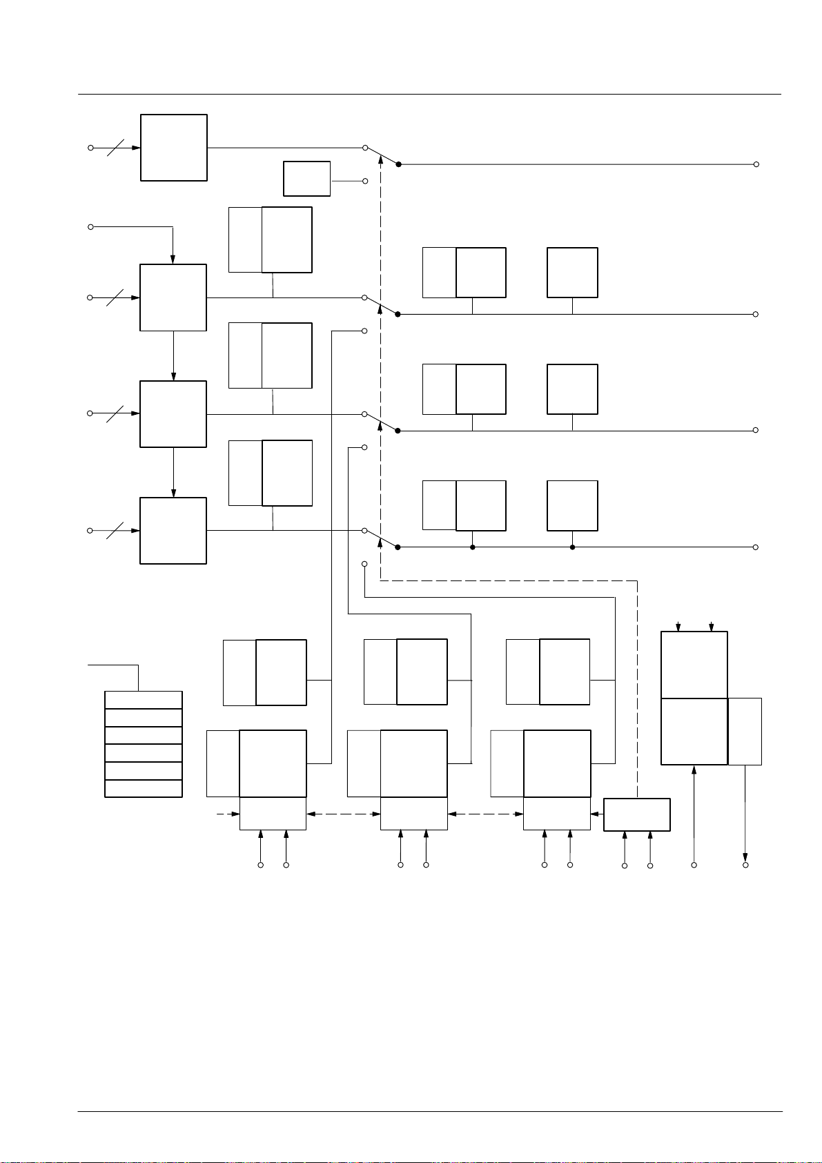
The digital RGB signals are converted to analog RGBs
using three video digital to analog converters (DAC) with
10-bit resolution. An analog brightness value is provided
by three additional DACs. The adjustment range is 40%
of the full RGB range.
Controlling the whitedrive/analog brightness and also
the external contrast and brightness adjustments is
done via the Fast Processor, located in the front-end.
Control of the cutoff DACs is via I
2
C-bus registers.
Finally cutoff and blanking values are added to the RGB
signals. Cutoff (dark current) is provided by three 9-bit
DACs. The adjustment range is 60% of full scale RGB
range.
The analog RGB-outputs are current outputs with current-sink characteristics. The maximum current drawn
by the output stage is obtained with peak white RGB. An
external half contrast signal can be used to reduce the
output current of the RGB outputs to 50%.
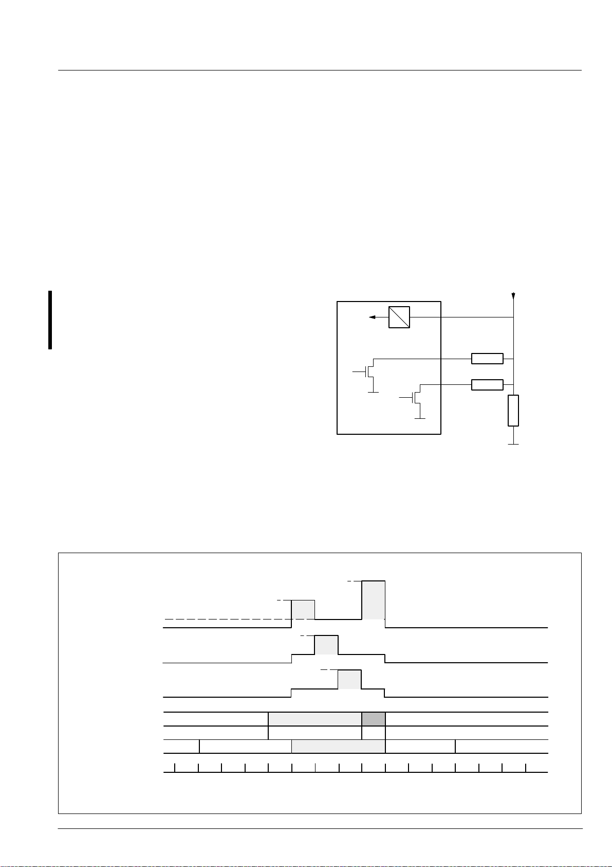
2.9.1. CRT Measurement and Control
The display processor is equipped with an 8-bit PDMADC for all measuring purposes. The ADC is connected
to the sense input pin, the input range is 0 to 1.5V. The
bandwidth of the PDM filter can be selected; it is
40/80 kHz for small/large bandwidth setting. The input
impedance is more than 1 MΩ.
Cutoff and white drive current measurement are carried
out during the vertical blanking interval. They always use
the small bandwidth setting. The current range for the
cutoff measurement is set by connecting a sense resistor to the MADC input. For the whitedrive measurement,
the range is set by using another sense resistor and the
range select switch 2 output pin (RSW2). During the active picture, the minimum and maximum beam current
is measured. The measurement range can be set by using the range select switch 1 pin (RSW1) as shown in
Fig. 2–21 and Fig. 2–22. The timing window of this measurement is programmable. The intention is to automatically detect letterbox transmission or to measure the actual beam current. All control loops are closed via the
external control microprocessor.
beam current
A
SENSE
D
MADC
RSW1
RSW2
R2
R3
R1
Fig. 2–21: MADC Range Switches
CR + IBRM
black
ultra black
active
measurement
resistor
PICTURE MEAS.
Lines
R1øR2øR3
RSW1=on, RSW2=on
PMSO
Fig. 2–22: MADC Measurement Timing
CR + IBRM + WDRV·WDR
cutoff
R
CG + IBRM
CB + IBRM
TUBE MEASUREMENT
TML
R1
cutoff
G
cutoff
B
white
drive
R
R1øR3
RSW2
=on
R
G
B
R1øR2øR3
RSW1=on, RSW2=on
PICTURE MEAS.
PMST
21Micronas
Page 22
PRELIMINARY DATA SHEETVDP 31xxB
In each field two sets of measurements can be taken:
a) The picture tube measurement returns results for
– cutoff R
– cutoff G
– cutoff B
– white drive R or G or B (sequentially)
b) The picture measurement returns data on
– active picture maximum current
– active picture minimum current
The tube measurement is automatically started when
the cutoff blue result register is read. Cutoff control for
RGB requires one field only while a complete white-drive
control requires three fields. If the measurement mode
is set to ‘offset check’, a measurement cycle is run with
the cutoff/whitedrive signals set to zero. This allows to
compensate the MADC offset as well as input the
leakage currents. During cutoff and whitedrive measurements, the average beam current limiter function (ref.
2.9.3.) is switched off and a programmable value is used
for the brightness setting. The start line of the tube measurement can be programmed via I
2
C-bus, the first line
used for the measurement, i.e. measurement of cutoff
red, is 2 lines after the programmed start line.
The picture measurement must be enabled by the control microprocessor after reading the min./max. result
registers. If a ‘1’ is written into bit 2 in subaddress 25, the
measurement runs for one field. For the next measurement a ‘1’ has to be written again. The measurement is
always started at the beginning of active video.
The vertical timing for the picture measurement is programmable, and may even be a single line. Also the signal bandwidth is switchable for the picture measurement.
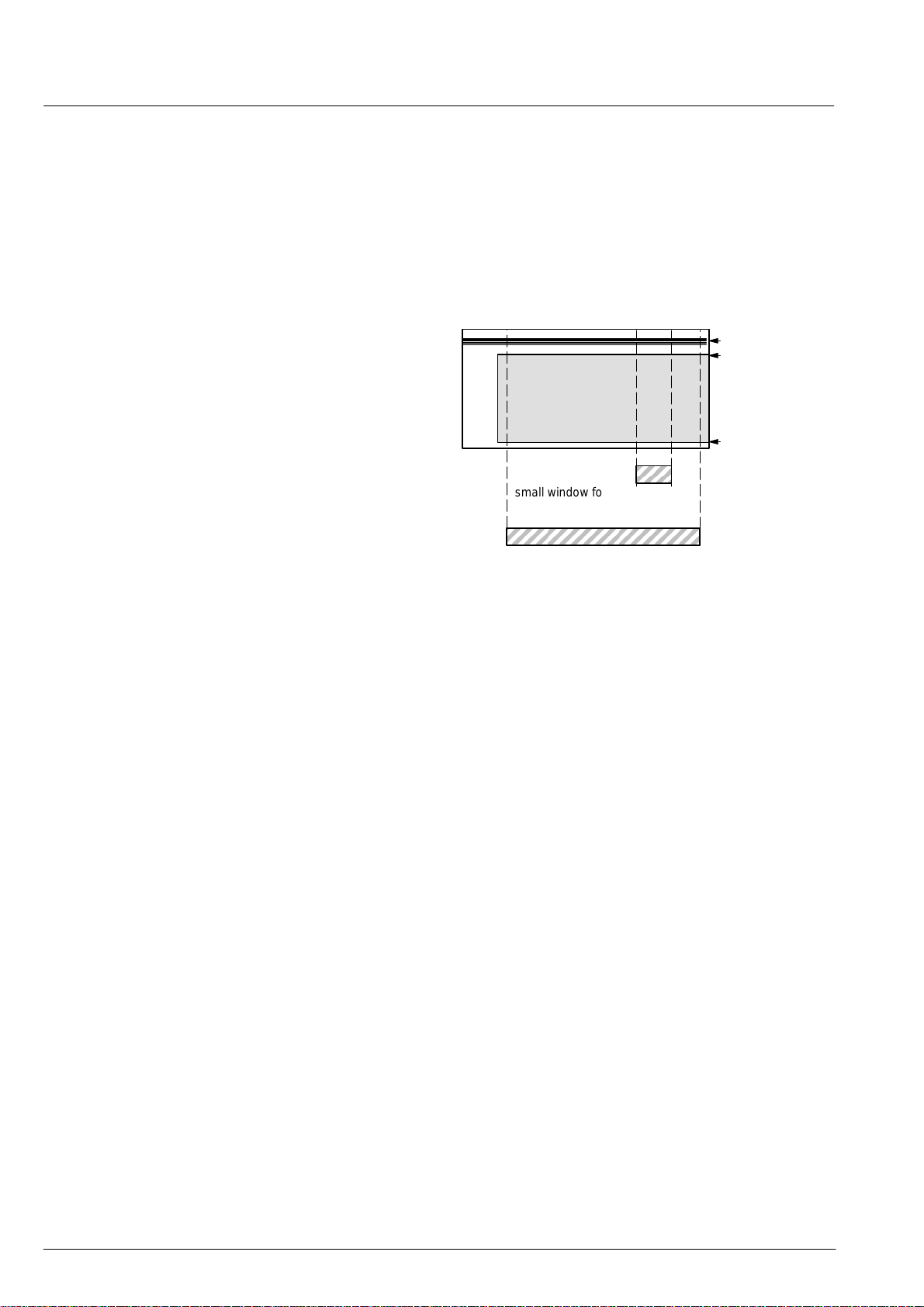
Two horizontal windows are available for the picture
measurement. The large window is active for the entire
active line. Tube measurement is always carried out with
the small window. Measurement windows for picture
and tube measurement are shown in Figure 2–23.
tube measurement
picture meas. start
active video
field 1/ 2
picture meas. end
small window for tube
measurement (cutoff, white drive)
large window for active picture
Fig. 2–23: Windows for tube and picture measure-
ments
2.9.2. SCART Output Signal
The RGB output of the VDP 31xxB can also be used to
drive a SCART output. In the case of the SCART signal,
the parameter CLMPR (clamping reference) has to be
set to 1. Then, during blanking, the RGB outputs are automatically set to 50% of the maximum brightness. The
DC offset values can be adjusted with the cutoff parameters CR, CG, and CB. The amplitudes can be adjusted
with the drive parameters WDR, WDG, and WDB.
22 Micronas
Page 23
PRELIMINARY DATA SHEET VDP 31xxB
2.9.3. Average Beam Current Limiter
The average beam current limiter (BCL) uses the sense
input for the beam current measurement. The BCL uses
a different filter to average the beam current during the
active picture. The filter bandwidth is approx. 2 kHz. The
beam current limiter has an automatic offset adjustment
that is active two lines before the first cutoff measurement line.
The beam current limiter function is located in the frontend. The data exchange between the front-end and the
back-end is done via a single-wire serial interface.
The beam current limiter allows the setting of a threshold
current. If the beam current is above the threshold, the
excess current is low-pass filtered and used to attenuate
the RGB outputs by adjusting the white-drive multipliers
for the internal (digital) RGB signals, and the analog contrast multipliers for the analog RGB inputs, respectively.
The lower limit of the attenuator is programmable, thus
a minimum contrast can always be set. During the tube
measurement, the ABL attenuation is switched off. After
the white drive measurement line it takes 3 lines to
switch back to BCL limited drives and brightness.
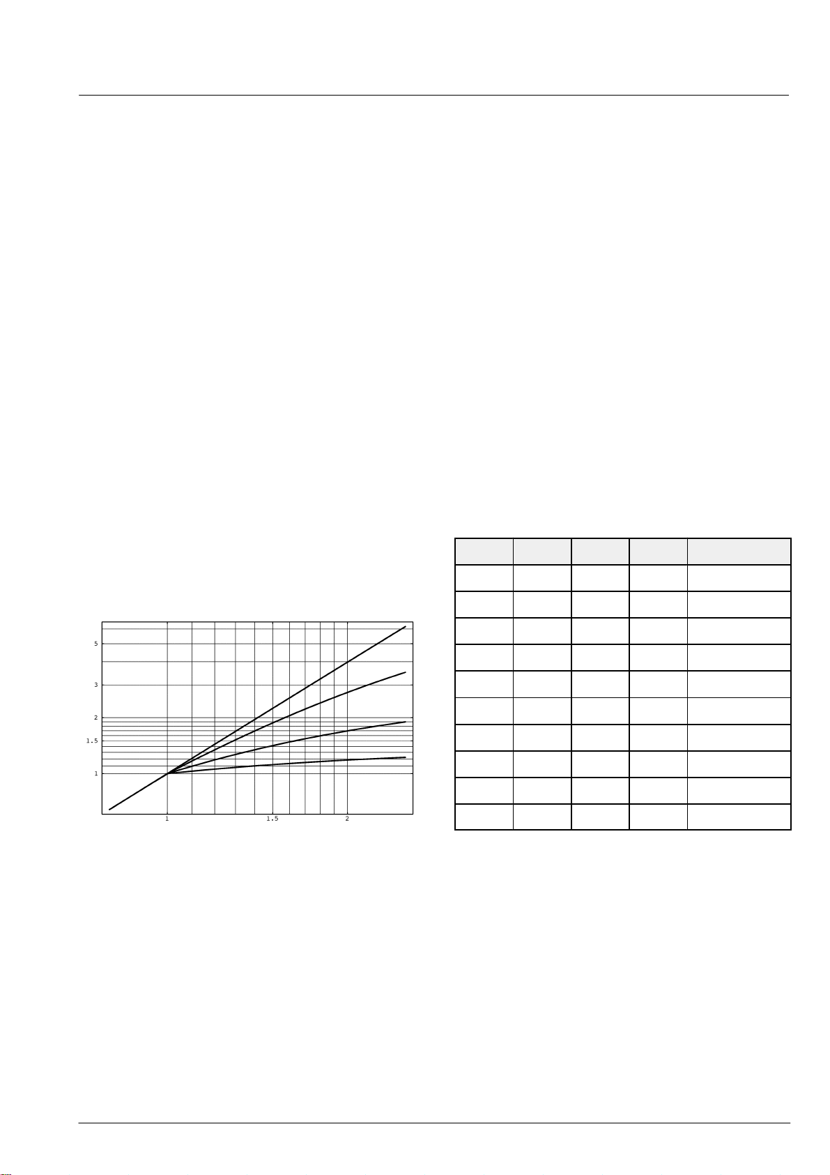
Typical characteristics of the ABL for dif ferent loop gains
are shown in Fig. 2–24; for this example the tube has
been assumed to have square law characteristics.
2.9.4. Analog RGB Insertion
The VDP 31xxB allows insertion of 2 external analog
RGB signals. Each RGB signal is key-clamped and inserted into the main RGB by the fast blank switch. The
selected external RGB input is virtually handled as a
priority bus signal. Thus, it can be overlaid or underlaid
to the digital picture. The external RGB signals can be
adjusted independently as regards DC-level (brightness) and magnitude (contrast).
Which analog RGB input is selected depends on the fast
blank input signals and the programming of a number of
2
I
C-bus register settings (see T able 2–3 and Fig. 2–25).
Both fast blank inputs must be either active-low or active-high.
All signals for analog RGB insertion (RIN1/2, GIN1/2,
BIN1/2, FBLIN1/2, HCS) must be synchronized to the
horizontal flyback, otherwise a horizontal jitter will be visible. The VDP 31xxB has no means for timing correction
of the analog RGB input signals.
Table 2–3: RGB Input Selection
FBFOH1 = 0, FBFOH2 = 0, FBFOL1 = 0, FBFOL2 = 0
FBLIN1 FBLIN2 FBPOL FBPRIO RGB output
0 0 0 x Video
beam current
drive
Fig. 2–24: Beam current limiter characteristics:
beam current output vs. drive
BCL threshold: 1
0 1 0 x RGB input 2
1 0 0 x RGB input 1
1 1 0 0 RGB input 1
1 1 0 1 RGB input 2
0 0 1 0 RGB input 1
0 0 1 1 RGB input 2
0 1 1 x RGB input 1
1 0 1 x RGB input 2
1 1 1 x Video
23Micronas
Page 24
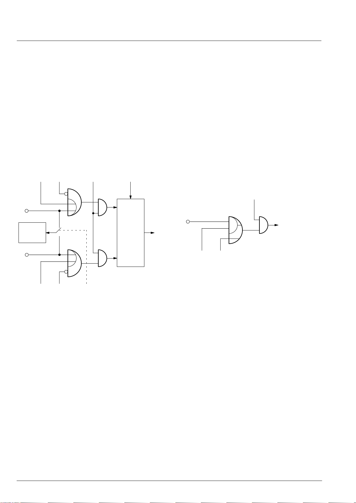
PRELIMINARY DATA SHEETVDP 31xxB
2.9.5. Fast Blank Monitor
The presence of external analog RGB sources can be
detected by means of a fast blank monitor. The status of
the selected fast blank input can be monitored via an I
2
bus register. There is a 2 bit information, giving static and
dynamic indication of a fast blank signal. The static bit is
directly reading the fast blank input line, whereas the dynamic bit is reading the status of a flip-flop triggered by
the negative edge of the fast blank signal.
With this monitor logic it is possible to detect if there is
an external RGB source active and if it is a full screen insertion or only a box. The monitor logic is connected directly to the FBLIN1 or FBLIN2 pin. Selection is done via
2
I
C bus register.
FBFOH1 FBPRIO
FBLIN1
Fast
Blank
Monitor
FBFOL1
FBPOL
#
Fast
Blank
Selection
FB
int
2.9.6. Half Contrast Control
Insertion of transparent text pages or OSD onto the video picture is often difficult to read, especially if the video
C
contrast is high. The VDP 31xxB allows contrast reduction of the video background by means of a half contrast
input (HCS pin). This input can be supplied with a fast
switching signal (similar to the fast blank input), typically
defining a rectangular box in which the video picture is
displayed with reduced contrast. The analog RGB inputs
are still displayed with full contrast.
The HCS input is multiplexed with the PORT0 input/output on the same pin, selection is done via I
2
C-bus register. If the HCS input is selected, then the port function of
this pin is disabled and writing data into PORT0 will have
no effect. If the HCS input is not selected, the I
2
C-bus
register bits HCSFOH and HCSPOL must be used to
disable the half contrast function.
HCSPOL
HCS
#
HCS intern
FBLIN2
#
FBFOH2 FBMON
FBFOL2
Fig. 2–25: Fast Blank Selection Logic
HCSEN HCSFOH
Fig. 2–26: Half Contrast Switch Logic
2.10. IO Port Expander
The VDP 31xxB provides a general purpose IO port to
control and monitor up to seven external signals. The
port direction is programmable for each bit individually.
2
Via I
C bus register it is possible to write or read each
port pin. Because of the relatively low I
2
C bus speed,
only slow or static signals can be handled.
The port signals are multiplexed with other signals to
minimize pin count. PORT0 is multiplexed with the HCS
input signal, PORT1 is multiplexed with the FSY output
signal, PORT[6:2] are multiplexed with the color bus input COLOR[4:0]. The pin configuration is programmable
2
via I
C bus register. All register bits can be read back, the
default configuration after reset is input on PORT[1:0]
and COLOR[4:0] enabled.
24 Micronas
Page 25
PRELIMINARY DATA SHEET VDP 31xxB
t
digital
SVM in
HCS
digital
R in
digital
G in
digital
B in
10
8 bit
DAC
SVM
8
1.88mA
analog
SVM ou
0.94mA
9 bit
DAC
10 bit
DAC
Video
1.5 mA
white drive R
int. brightness *
cutoff R
9 bit
DAC
2.2 mA
blanking
750 µA
analog
R out
3.75mA
9 bit
10
10 bit
DAC
Video
3.75mA
DAC
1.5 mA
white drive G
int. brightness *
cutoff G
9 bit
DAC
2.2 mA
blanking
750 µA
analog
G out
9 bit
DAC
10
10 bit
DAC
Video
3.75mA
1.5 mA
int. brightness *
white drive B
cutoff B
9 bit
DAC
2.2 mA
blanking
750 µA
analog
B out
serial interface
white drive R
white drive G
white drive B
int . brightness
ext. contrast
ext. brightness
ext. brightness *
ext. contrast *
white drive R *
beam current lim.
key
Fig. 2–27: Analog back-end
9 bit
DAC
1.5 mA
white drive R
9 bit
U/I–DAC
3.75mA
clamp
& mux
12
analog
R in
9 bit
DAC
1.5 mA
white drive G
ext. brightness *
9 bit
U/I–DAC
3.75mA
ext. contrast *
white drive G *
beam current lim.
clamp
& mux
ext. contrast *
12 12
analog
G in
1.5 mA
white drive B
ext. brightness *
9 bit
U/I–DAC
3.75mA
white drive B *
beam current lim.
clamp
& mux
analog
B in
9 bit
DAC
FBL
prio
12
fast
blank in
V
H
blank &
measurem.
timing
8 bit
ADC
measurm.
Sense
Input
buffer
measurement
I/O
25Micronas
Page 26

VDP 31xxB PRELIMINARY DATA SHEET
2.11. Synchronization and Deflection
The synchronization and deflection processing is
distributed over front-end and back-end. The video
clamping, horizontal and vertical sync separation and all
video related timing information are processed in the
front-end. Most of the processing that runs at the horizontal frequency is programmed on the internal Fast
Processor (FP). Also the values for vertical and East/
West deflection are calculated by the FP software.
The information extracted by the video sync processing
is multiplexed onto the hardware front sync signal (FSY)
and distributed internally to the rest of the video processing system.
The data for the vertical deflection, the sawtooth and the
East/West correction signal is calculated in the front
end. The data is transferred to the back-end by a single
wire interface.
The display related synchronization, i.e. generation of
horizontal and vertical drive and synchronization of horizontal and vertical drive to the video timing extracted in
the front-end, are implemented in hardware in the backend.
2.11.1. Deflection Processing
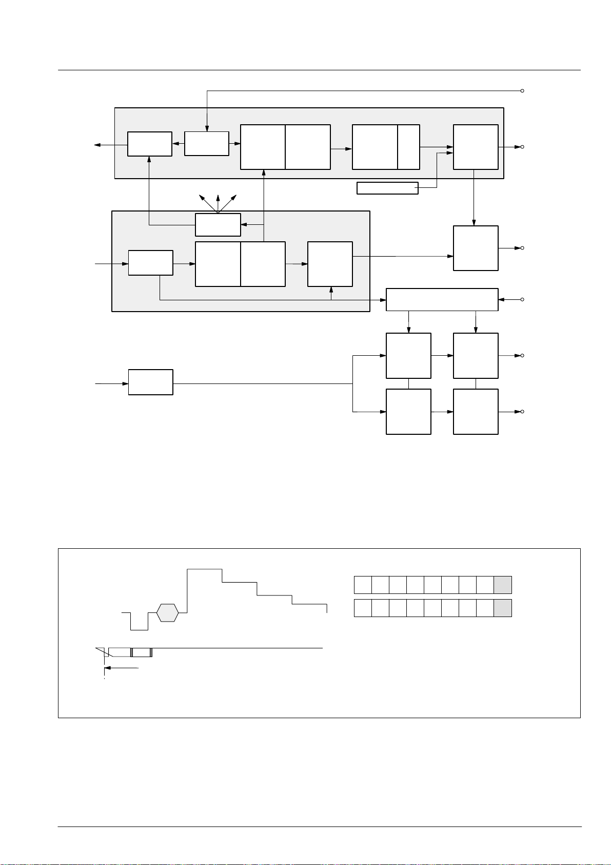
The deflection processing generates the signals for the
horizontal and vertical drive (see Fig. 2–28). This block
contains two phase-locked loops:
– PLL2 generates the horizontal and vertical timing, e.g.
blanking, clamping and composite sync. Phase and
frequency are synchronized by the front sync signal.
– PLL3 adjusts the phase of the horizontal drive pulse
and compensates for the delay of the horizontal output
stage. Phase and frequency are synchronized by the
oscillator signal of PLL2.
The horizontal drive circuitry uses a digital sine wave
generator to produce the exact (subclock) timing for the
drive pulse. The generator runs at 1 MHz; in the output
stage the frequency is divided down to give drive-pulse
period and width. In standby mode, the output stage is
driven from an internal 1 MHz clock that is derived from
the 5 MHz clock signal and a fixed drive pulse width is
used. When the circuit is switched out of standby
operation, the drive pulse width is programmable. The
horizontal drive uses an open drain output transistor.
The Main Sync (MSY) signal that is generated from
PLL3 is a multiplex of all display-related data
(Fig. 2–29). This signal is intended for use by other processors, e.g. a PIP processor can use this signal to adjust to a certain display position.
2.11.2. Horizontal Phase Adjustment
This section describes a simple way to align PLL phases
and the horizontal frame position.
1. The parameter NEWLIN in the front-end has to be
adjusted. The minimum possible value is 34 (recommended for a standard 4:3 signal).
2. With HDRV, the duration of the horizontal drive pulse
has to be adjusted.
3. With POFS2, the clamping pulse for the analog RGB
input has to be adjusted to the correct position, e.g.
the pedestal of the generator signal.
4. With POFS3, the horizontal position of the analog
RGB signal (from SCART) has to be adjusted.
5. With HPOS, the digital RGB output signal (from VPC)
has to be adjusted to the correct horizontal position.
6. With HBST and HBSO, the start and stop values for
the horizontal blanking have to be adjusted.
Note: The processing delay of the internal digital video
path differs depending on the comb filter option of the
VDP 31xxB. The versions with comb filter have an additional delay of 35 clock cycles. Therefore, the timing of
the external analog RGB signals has to be adjusted (with
POFS2 and POFS3) according to the actual hardware
version of the VDP 31xxB. The hardware version can be
read out via FP subaddress 0xF1.
26 Micronas
Page 27
PLL3
VDP 31xxBPRELIMINARY DATA SHEET
H
flyback
MSY
FSY
VDATA
main
sync
generator
front
sync
interface
vertical
serial
data
skew
measure–
ment
phase
comparator
lowpass
blanking, clamping, etc.
display
timing
phase
comparator
&
lowpass
DCO
vertical reset
&
DCO
sinewave
generator
DAC
&
LPF
1:64
&
output
stage
H
drive
Standby clock
PLL2
composite
line
counter
clock & control
E/W
correction
sawtooth
sync
generator
PWM
15 bit
PWM
15 bit
CSY
V
flyback
E/W
ouput
V
output
Fig. 2–28: Deflection processing block diagram
input
analog
video
MSY
M1 M2
timing reference for PICTURE bus
(not in scale)
– chroma multiplex sync
– active picture data after xxx clocks
Fig. 2–29: Main sync format
M1
M2
line
line
line
[0]
not
[8]
used
not
used
not
used
not
used
used
not
V: Vert. blanking
F: Field #
line: Field line #
[7]
F
0 = off
1 = on
0 = Field 1
1 = Field 2
1...N
Parity
V
Parity
27Micronas
Page 28
VDP 31xxB PRELIMINARY DATA SHEET
2.11.3. Vertical and East/West Deflection
The calculations of the vertical and East/West deflection
waveforms is done by the internal Fast Processor (FP).
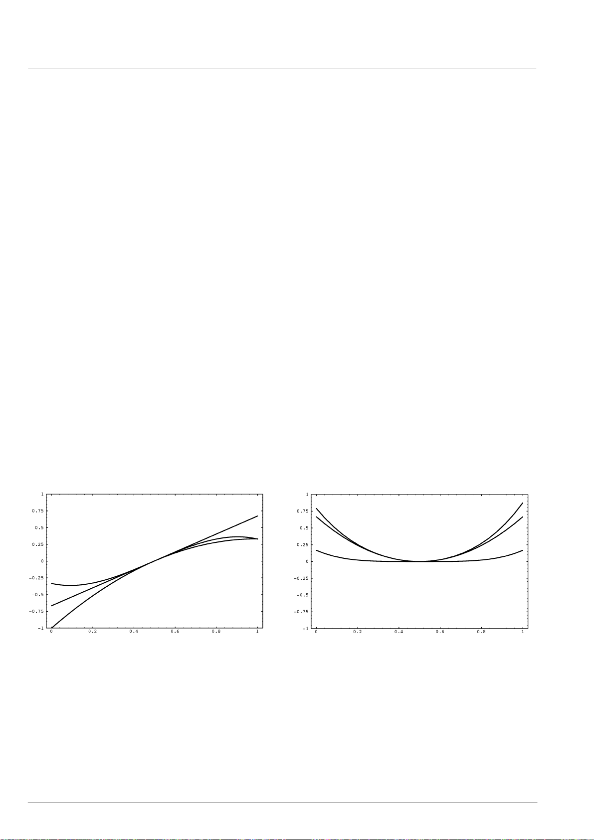
The algorithm uses a chain of accumulators to generate
the required polynomial waveforms. To produce the
deflection waveforms, the accumulators are initialized at
the beginning of each field. The initialization values must
be computed by the TV control processor and are written
to the front-end once. The waveforms are described as
polynomials in x, where x varies from 0 to 1 for one field.
P: a + b(x–0.5) + c(x–0.5)
2
+ d(x–0.5)3 + e(x–0.5)
4
The initialization values for the accumulators a0..a3 for
vertical deflection and a0..a4 for East/West deflection
are 12-bit values.
The vertical waveform can be scaled according the
average beam current. This is used to compensate the
effects of electric high tension changes due to beam current variations. In order to get a faster vertical retrace
timing, the output impedance of the vertical
D/A-converter can be reduced by 50% during the retrace.
2.11.4. Protection Circuitry
– Picture tube and drive stage protection is provided
through the following measures:
– Vertical flyback protection input: this pin searches for
a negative edge in every field, otherwise the RGB
drive signals are blanked.
– Drive shutoff during flyback: this feature can be se-
lected by software.
– Safety input pin: this input has two thresholds. Be-
tween zero and the lower threshold, normal functioning takes place. Between the lower and the higher
threshold, the RGB signals are blanked. Above the
higher threshold, the RGB signals are blanked and the
horizontal drive is shut off. Both thresholds have a
small hysteresis.
– The main oscillator and the horizontal drive circuitry
are run from a separate (standby) power supply and
are already active while the TV set is powering up.
Fig. 2–30 shows several vertical and East/West deflection waveforms. The polynomial coefficients are also
stated.
Vertical: a,b,c,d
0,1,0,0
0,1,1,0
0,1,0,1
East/West: a,b,c,d,e
0,0,1,0,0
0,0,0,0,1
0,0,1,1,1
Fig. 2–30: Vertical and East/West deflection waveforms
28 Micronas
Page 29
PRELIMINARY DATA SHEET VDP 31xxB
2.12. Reset Function
Reset of most VDP 31xxB functions is performed by the
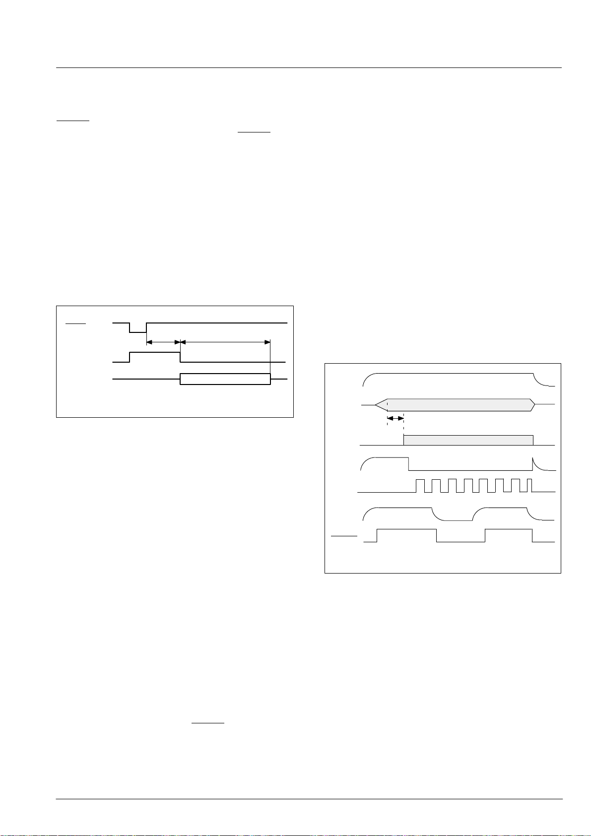
RESET
registers and counters are lost. When the RESET
pin. When this pin becomes active, all internal
pin is
released, the internal reset is still active for 4 µs. After
that time, the initialization of all required registers is performed by the internal Fast Processor. During this initialization procedure (see Fig. 2–31) it is not possible to ac-
cess the VDP 31xxB via the serial interface (I
2
C).
Access to other ICs via the serial bus is possible during
that time.
The 5 MHz clock divider and the 1 MHz standby clock divider are not affected by reset. The clock source for the
horizontal output generator is switched to the standby
clock during reset.
Reset
Internal
Reset
4µs
approx. 60µs
In the standby mode the following functions are still
available (see also 2.11.1.):
– 20.25 MHz crystal oscillator
– 5 MHz clock output (CLK5)
– horizontal drive output (HOUT)
The clock source for the horizontal output generator is
switched to the standby clock which is derived from the
5 MHz clock. The duty cycle of HOUT is set to 50%.
Protection modes with safety and horizontal flyback pins
are not available.
The VDP 31xxB has clock and voltage supervision circuits to generate a stable HOUT signal during power-on
and standby . The HOUT signal is disabled until a proper
CLK5 signal (5 MHz clock) is detected. When released,
the HOUT generator runs with the standby clock. Coupling the HOUT generator to the deflection PLL has to
be done by CCU using the EHPLL bit. Fig. 2–32 shows
the signals during power-on and standby.
Initialization
Fig. 2–31: External Reset
2.13. Standby and Power-On
In standby mode the whole signal processing of the VDP
31xxB is disabled and only some basic functions are
working. The standby mode is realized by switching off
the supplies for analog front-end (VSUPF), analog backend (VSUPO) and digital circuitry (VSUPD). The standby supply (VSTBY) still has its nominal voltage.
T o disable all the analog and digital functions, it is necessary to bring the analog and digital supplies below 0.5 V .
Only this guarantees that all the normal functions are
disabled and the standby current for analog and digital
supply is at its minimum.
When switched off, the negative slope of the supply
voltage VSUPD should not be larger than approximately
0.2 V/µs (see Recommended Operating Conditions).
In the standby mode, all registers and counter values in
the VDP 31xxB are lost, they will be re-initialized via the
internal Fast Processor after analog and digital supplies
are switched on again and the RESET
pin is released.
VSTBY
XTAL
1 µs
CLK5
Clock
Release
HOUT
VSUP
RESET
D
standby
mode
Fig. 2–32: Power-On, Standby On/Off
Switching the HOUT signal into standby mode can be
done by the CCU via the EHPLL bit or by the internal voltage supervision. The voltage supervision activates a
power-down signal when the supply for the digital circuits (VSUPD) goes below X4.5 V for more than 50ns.
This power down signal is extended by 50µs after
VSUPD is back again. The power-down signal switches
the clock source for the HOUT generation to the standby
clock and sets the duty cycle to 50%. This is exactly what
the EHPLL bit does.
As the clocks from the deflection PLL and the standby
clock are not in phase, the actual phase (High/Low) of
the HOUT signal may be up to one PLL or standby clock
(X1 µs) longer than a regular one when the clock source
is changed.
29Micronas
Page 30
VDP 31xxB PRELIMINARY DATA SHEET
3. Serial Interface
3.1. I2C-Bus Interface
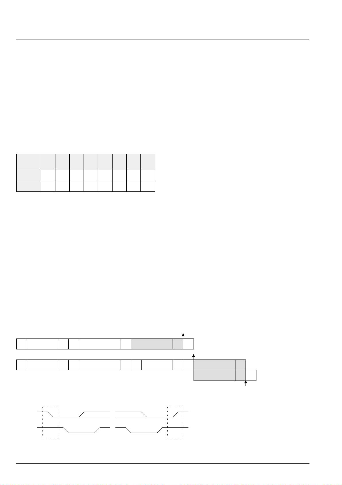
Communication between the VDP and the external controller is done via I2C-bus. The VDP has two I2C-bus
slave interfaces (for compatibility with VPC/DDP applications) – one in the front-end and one in the back-
end. Both I
tion to slow down the interface if required. Both I
interfaces use one level of subaddress: the I
2
C-bus interfaces use I2C clock synchroniza-
2
C-bus
2
C-bus chip
address is used to address the IC and a subaddress selects one of the internal registers. The I
2
C-bus chip ad-
dresses are given below:
Chip
Address
front-end 1 0 0 0 1 1 1 1/0
back-end 1 0 0 0 1 0 1 1/0
A6 A5 A4 A3 A2 A1 A0 R/W
The registers of the VDP have 8 or 16-bit data size;
16-bit registers are accessed by reading/writing two
8-bit data words.
Figure 3–1 shows I
2
C-bus protocols for read and write
operations of the interface; the read operation requires
an extra start condition and repetition of the chip address
with read command set.
3.2. Control and Status Registers
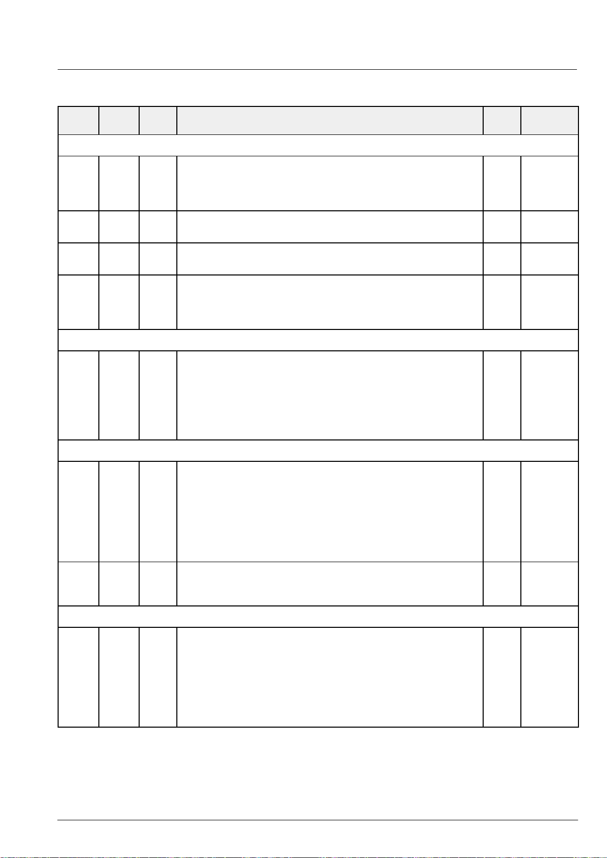
T able 3–1 gives definitions of the VDP control and status
registers. The number of bits indicated for each register
in the table is the number of bits implemented in hardware, i.e. a 9-bit register must always be accessed using
two data bytes but the 7 MSB will be ‘don’t care’ on write
operations and ‘0’ on read operations. Write registers
that can be read back are indicated in Table 3–1.
Functions implemented by software in the on-chip control microprocessor (FP) are explained in Table 3–3.
A hardware reset initializes all control registers to 0. The
automatic chip initialization loads a selected set of registers with the default values given in Table 3–1.
The register modes given in Table 3–1 are
– w: write only register
– w/r: write/read data register
– r: read data from VDP
– v: register is latched with vertical sync
– h: register is latched with horizontal sync
The mnemonics used in the Micronas VDP demo software are given in the last column.
S
1000 111
WP1 or 2 byte Data
Ack
0111 1100
Ack
Ack
I2C write access
subaddress 7c
2
C read access
S
1000 111 1000 111
SDA
SCL
W high byte Data
Ack
0111 1100 RS Ack
Ack
1
SP
0
Ack
Nak
W= 0
R=1
Ack = 0
Nak = 1
S = Start
I
subaddress 7c
Plow byte Data
P = Stop
Fig. 3–1: I2C-bus protocols
30 Micronas
Page 31
PRELIMINARY DATA SHEET VDP 31xxB
Table 3–1: I2C control and status registers of front-end
I2C Sub
address
Number
of bits
Mode Function Default Name
FP INTERFACE
h’35 8 r FP status
bit [0] write request
bit [1] read request
bit [2] busy
h’36 16 w bit[8:0] 9-bit FP read address
bit[11:9] reserved, set to zero
h’37 16 w bit[8:0] 9-bit FP write address
bit[11:9] reserved, set to zero
h’38 16 w/r bit[11:0] FP data register, reading/writing to this
register will autoincrement the FP read/
write address. Only 16 bit of data are
2
transferred per I
C telegram.
BLACK LINE DETECTOR
h’12 16 w/r read only register, do not write to this register!
after reading, LOWLIN and UPLIN are reset to 127 to start a new
measurement
bit[6:0] number of lower black lines
bit[7] always 0
bit[14:8] number of upper black lines
bit[15] 0/1 normal/black picture
FPSTA
FPRD
FPWR
FPDAT
BLKLIN
LOWLIN
UPLIN
BLKPIC
PIN CIRCUITS
h’1F 16 w/r INTLC & PORT pins:
bit[2:0] 0..7 output strength for INTLC & PORT Pins
(7 = tristate, 6 = weak ... 0 = strong)
bit[3] 0 reserved (set to 0)
bit[4] 0/1 pushpull/tristate for INTLC Pin
bit[5] 0/1 synchronization/no synchronization with
horizontal MSY for signal INTLC
bit[15:6] reserved (set to 0)
h’20 8 w/r SYNC GENERA TOR CONTROL:
bit[6:0] 0 reserved (set to 0)
bit[7] 0/1 positive/negative polarity for INTLC signal
PRIORITY BUS
h’24 8 w/r priority bus ID register and control
bit [2:0] 0..7 priority ID, 0 highest
bit [4:3] 0..3 pad driver strength, 0 (strong) to 3 (weak)
bit [5] 0/1 reserved (set to 0)
bit [6] 0/1 source for prio request:
active video/clamp_to_1
bit [7] 0/1 disable/enable priority interface, if disabled
frontend is disconnected from priority bus!
0
0
0
0
0
0
0
0
0
TRPAD
SNCSTR
SNCDIS
VASYSEL
SYNMODE
INTLCINV
PRIOMODE
PID
PRIOSTR
PIDSRC
PIDE
31Micronas
Page 32
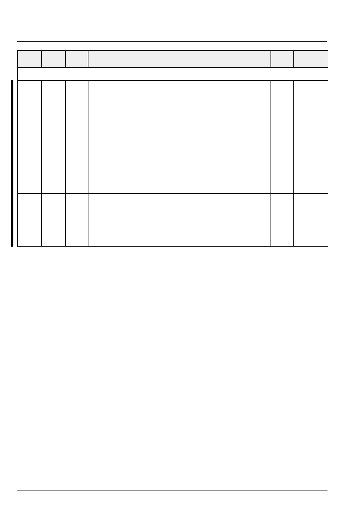
VDP 31xxB PRELIMINARY DATA SHEET
I2C Sub
address
of bits
SYNC GENERATOR
h’21 16 w/r LINE LENGTH:
bit[10:0] LINE LENGTH register
bit[15:11] reserved (set to 0)
h’29 16 w/r AVO STOP:
bit[10:0] reserved (set to 0)
bit[11] 0/1 disable/enable test pattern generator
bit[13:12] luma output mode:
bit[14] 0/1 reserved (set to 0)
bit[15] 0/1 chroma output: pseudo color bar/zero
h’22 16 w/r NEWLINE:
bit[10:0] NEWLINE register
bit [15:11] reserved (set to 0)
LINE LENGTH has to be set to 1295 for
correct adjustment of vertical signals.
00 Y = rampe (240 ... 17)
01 Y = 16
10 Y = 90
11 Y = 240
This register defines the readout start of
the next line in respect to the value of the
sync counter. Value of this register must
be greater than 31 for correct operation.
1295
50
0
0
0
0
0
NameDefaultFunctionModeNumber
LINLEN
AVSTOP
COLBAREN
LMODE
CMODE
NEWLIN
32 Micronas
Page 33
Table 3–2: Backend I2C-control and status registers
VDP 31xxBPRELIMINARY DATA SHEET
I2C sub
address
Number
of bits
Mode Function Default Name
PRIORITY BUS
priority mask register, if bit[x] is set to 1 then the function is
active for the respective signal priority
h’75 9 w v bit [7:0] bit[x] 0/1: select contrast,brightness,matrix
0 PBCT
for main/side picture
h’71 9 w v bit [7:0] bit[x] 0/1: select main (video)/external (via CLUT)
0 PBERGB
RGB
h’7d 9 w v bit [7:0] bit[x] 0/1: enable/disable black level expander 0 PBBLE
h’79 9 w v bit [7:0] bit[x] 0/1: disable/enable peaking transient
0 PBPK
suppression when signal is switched
h’4b 9 w v bit [7:0] bit[x] 0/1: disable/enable analog fast blank input 0 PBFB
h’47 9 w v bit [2:0] picture frame generator priority id
bit [8] enable prio id for picture frame generator
0 PFGID
PFGEN
LUMA CHANNEL
h’61 9 w v bit [5:0] 0..63/32 main picture contrast 32 CTM
h’65 9 w v bit [5:0] 0..63/32 side picture contrast 32 CTS
h’51 9 w v bit [8:0] –256..255 main picture brightness 0 BRM
h’55 9 w v bit [8:0] –256..255 side picture brightness 0 BRS
h’59 9 w v black level expander:
BTLT
12
8
BAM
bit [3:0] 0..15 tilt coefficient
bit [8:4] 0...31 amount
h’5d 9 w v black level expander:
bit [8:0] 0..511 disable expansion, threshold value
200
BTHR
h’69 9 w v luma peaking filter, the gain at high frequencies and small signal
amplitudes is: 1 + (k1+k2)/8
PKUN
bit [3:0] 0..15 k1: peaking level undershoot
bit [7:4] 0..15 k2: peaking level overshoot
bit [8] 0/1 peaking value normal/inverted
4
4
0
PKOV
PKINV
(peaking/softening)
h’6d 9 w v luma peaking filter, coring
COR
bit [4:0] 0..31 coring level
3
bit [7:5] reserved
PFS
bit [8] 0/1 peaking filter center frequency high/low
0
h’41 9 w v luma soft limiter, slope A and B
LSLSA
bit [3:0] slope segment A
bit [7:4] slope segment B
0
0
LSLSB
h’45 9 w v bit [7:0] luma soft limiter absolute limit (unsigned)
bit [8] 0/1 modulation off/on
2551LSLAL
LSLM
h’49 9 w v bit [8:0] luma soft limiter segment B tilt point (unsigned) 300 LSLTB
h’4d 9 w v bit [8:0] luma soft limiter segment A tilt point (unsigned) 250 LSLTA
33Micronas
Page 34
VDP 31xxB PRELIMINARY DATA SHEET
I2C sub
address
of bits
CHROMA CHANNEL
h’14 8 w/r luma/chroma matching delay
bit [2:0] –3...3 variable chroma delay
bit [3] 0/1 chroma polarity signed / offset binary
bit [4] 0/1 C
(U) sample first / CR (V) sample first
B
bit [7:5] reserved, set to 0
h’66 9 w v digital transient improvement
bit [3:0] 0..15 coring value
bit [7:4] 0..15 DTI gain
bit [8] 0/1 narrow/wide bandwidth mode
INVERSE MA TRIX
main picture matrix coefficient R–Y = MR1M*CB + MR2M*C
h’7c
h’74
9
9
w v
w v
bit [8:0] –256/128 ... 255/128
bit [8:0] –256/128 ... 255/128
main picture matrix coefficient G–Y = MG1M*CB + MG2M*C
h’6c
h’64
9
9
w v
w v
bit [8:0] –256/128 ... 255/128
bit [8:0] –256/128 ... 255/128
main picture matrix coefficient B–Y = MB1M*CB + MB2M*C
h’5c
h’54
9
9
w v
w v
bit [8:0] –256/128 ... 255/128
bit [8:0] –256/128 ... 255/128
NameDefaultFunctionModeNumber
0
LDB
1
COB
0
ENVU
0
DTICO
1
DTIGA
5
DTIMO
1
R
R
–22
–44
R
113
86
0
0
MR1M,
MR2M
MG1M,
MG2M
MB1M,
MB2M
h’78
h’70
h’68
h’60
h’58
h’50
h’00–
h’0f
side picture matrix coefficient R–Y = MR1S*CB + MR2S*C
9
9
w v
w v
bit [8:0] –256/128 ... 255/128
bit [8:0] –256/128 ... 255/128
side picture matrix coefficient G–Y = MG1S*CB + MG2S*C
9
9
w v
w v
bit [8:0] –256/128 ... 255/128
bit [8:0] –256/128 ... 255/128
side picture matrix coefficient B–Y = MB1S*CB + MB2S*C
9
9
w v
w v
bit [8:0] –256/128 ... 255/128
bit [8:0] –256/128 ... 255/128
COLOR LOOK-UP T ABLE
color look-up table : 16 entries, 12 bit wide,
The CLUT registers are initialized at power-up
16 w h
bit [3:0] 0..15 blue amplitude
bit [7:4] 0..15 green amplitude
bit [11:8] 0..15 red amplitude
R
R
–19
–37
R
000h
73
97
0
0
MR1S,
MR2S
MG1S,
MG2S
MB1S,
MB2S
CLUT0
f00h
0f0h
ff0h
00fh
f0fh
0ffh
fffh
7ffh
700h
070h
770h
007h
707h
077h
777h
CLUT15
picture frame color 12 bit wide,
h’11 16 w h
bit [3:0] 0..15 blue amplitude
bit [7:4] 0..15 green amplitude
bit [11:8] 0..15 red amplitude
PFCB
0
PFCG
0
PFCR
0
34 Micronas
Page 35
VDP 31xxBPRELIMINARY DATA SHEET
I2C sub
address
h’4c 9 w v
h’48 9 w v
h’44 9 w v
h’4F 9 w v bit [8:0] horizontal picture frame begin
of bits
digital OSD insertion contrast for R (amplitude range: 0 to 255)
bit [3:0] 0..13 R amplitude = CLUTn · (DRCT + 4)
14,15 invalid
picture frame insertion contrast for R (ampl. range: 0 to 255)
bit [7:4] 0..13 R amplitude = PFCR · (PFRCT + 4)
14,15 invalid
digital OSD insertion contrast for G (amplitude range: 0 to 255)
bit [3:0] 0..13 G amplitude = CLUTn · (DGCT + 4)
14,15 invalid
picture frame insertion contrast for G (ampl. range: 0 to 255)
bit [7:4] 0..13 G amplitude = PFCG · (PFGCT + 4)
14,15 invalid
digital OSD insertion contrast for B (amplitude range: 0 to 255)
bit [3:0] 0..13 B amplitude = CLUTn · (DBCT + 4)
14,15 invalid
picture frame insertion contrast for B (ampl. range: 0 to 255)
bit [7:4] 0..13 B amplitude = PFCB · (PFBCT + 4)
14,15 invalid
PICTURE FRAME GENERA T OR
code 0 = picture frame generator horizontally disabled
code 1FF = full frame
NameDefaultFunctionModeNumber
DRCT
8
PFRCT
8
DGCT
8
PFGCT
8
DBCT
8
PFBCT
8
0 PFGHB
h’53 9 w v bit [8:0] horizontal picture frame end 0 PFGHE
h’63 9 w v bit [8:0] vertical picture frame begin
code 0 = picture frame generator vertically disabled
h’6f 9 w v bit [8:0] vertical picture frame end 56 PFGVE
enable and priority – see under ‘PRIORITY BUS’
picture frame color – see under ‘COLOR LOOK-UP TABLE’
SCAN VELOCITY MODULA TION
h’62 9 w v video mode coefficients
bit [5:0] gain1
bit [8:6] differentiator delay 1 (0= filter off, 1...6= delay)
h’5e 9 w v text mode coefficients
bit [5:0] gain 2
bit [8:6] differentiator delay 2 (0= filter off, 1...6= delay)
h’5a 9 w v limiter
bit [6:0] limit value
bit [8:5] not used, set to ”0”
h’56 9 w v delay and coring
bit [3:0] adjustable delay, in 1/2 display clock steps,
(value 5 : delay of SVMOUT is the same as for
RGBOUT
bit [7:4] coring value
bit [8] not used, set to ”0”
270 PFGVB
SVG1
60
SVD1
4
SVG2
60
SVD2
4
0
7
0
SVLIM
SVDEL
SVCOR
100
35Micronas
Page 36
VDP 31xxB PRELIMINARY DATA SHEET
I2C sub
address
h’52
h’4e
h’4a
h’7b 9 w v picture measurement start line
h’6b 9 w v picture measurement stop line
h’7f 9 w v tube measurement line
h’25 8 w/r tube and picture measurement control
of bits
DISPLAY CONTROLS
9
9
9
TUBE AND PICTURE MEASUREMENT
w v
w v
w v
cutoff Red
cutoff Green
cutoff Blue
bit [8:0] (TML+9)..511 first line of picture measurement
bit [8:0] (PMST+1)..511 last line of picture measurement
bit [8:0] 0..511 start line for tube measurement
bit [0] 0/1 disable/enable tube measurement
bit [1] 0/1 80/40 kHz bandwidth for
bit [2] 0/1 disable/enable picture measurement
bit [3] 0/1 large/small picture measurement window,
bit [4] 0/1 measure / offset check for adc
bit [7:5] reserved
picture measurement
(writing a ’1’ starts one measurement
cycle)
will be disabled from bit[3] in address h’32
0
0
0
23
308
15
0 PMC
NameDefaultFunctionModeNumber
CR
CG
CB
PMST
PMSO
TML
TMEN
PMBW
PMEN
PMWIN
OFSEN
h’13 16 w/r white drive measurement control
bit [9:0] 0..1023 RGB values for white drive beam current
measurement
bit [10] reserved
bit [11] 0/1 RGB values for white drive beam current
measurement disabled/enabled
8 r measurement result registers
h’18
h’19
h’1a
h’1d
h’1c
h’1b
h’1e 8 r measurement adc status and fast blank input status
measurement status register
bit [0] 0/1 tube measurement active / complete
bit [2:1] white drive measurement cycle
00 red
01 green
10 blue
11 reserved
bit [3] 0/1 picture measurement active / complete
bit [4] 0/1 fast blank input low / high (static)
bit [5] 1 fast blank input negative transition since
bit [7:6] reserved
minimum in active picture
maximum in active picture
white drive
cutoff/leakage red
cutoff/leakage green
cutoff/leakage blue,
read pulse starts tube measurement
last read (bit reset at read)
512
0
–
– PMS
WDRV
EWDM
MRMIN
MRMAX
MRWDR
MRCR
MRCG
MRCB
36 Micronas
Page 37
VDP 31xxBPRELIMINARY DATA SHEET
I2C sub
address
of bits
NameDefaultFunctionModeNumber
TIMING
h’67 9 w v vertical blanking start
bit [8:0] 0..511 first line of vertical blanking
305
VBST
h’77 9 w v vertical blanking stop
VBSO
bit [8:0] 0..511 last line of vertical blanking
25
h’73 9 w v start of Black Level Expander measurement
AVST
bit [8:0] 0..511 first line of measurement, stop with first
30
line of vertical blanking
h’5f 9 w v bit [8:0] free running field period = (value)4) lines 0 STIMP
HORIZONT AL DEFLECTION
h’7a 9 w v adjustable delay of PLL2, clamping, and blanking (relative to
–141 POFS2
front sync)
adjust clamping pulse for analog RGB input
bit [8:0] –256..+255 " 8 µs
h’76 9 w v adjustable delay of flyback, main sync, csync and analog RGB
0 POFS3
(relative to PLL2)
adjust horizontal drive or csync
bit [8:0] –256..+255 "8 µs
h’7e 9 w v adjustable delay of main sync (relative to flyback)
adjust horizontal position for digital picture
bit [8:0] 20 steps+1 µs
h’5b 9 w/r start of horizontal blanking
bit [8:0] 0..511
h’57 9 w/r end of horizontal blanking
bit [8:0] 0..511
PLL2/3 filter coefficients, 1of5 bit code (n+ set bit number)
h’6a
h’6e
h’72
9
9
9
w v
w v
w v
bit [5:0] proportional coefficient PLL3, 2
bit [5:0] proportional coefficient PLL2, 2
bit [5:0] integral coefficient PLL2, 2
–n–1
–n–1
–n–5
h’15 16 w/r horizontal drive and vertical signal control register
bit [5:0] 0..63 horizontal drive pulse duration in ms
(internally limited to 4..61)
bit [6] 0/1 disable/enable horizontal PLL2 and PLL3
bit [7] 0/1 1: disable horizontal drive pulse during
flyback
bit [8] 0/1 reserved, set to ’0’
bit [9] 0/1 enable/disable ultra black blanking
bit [10] 0/1 0: all outputs blanked
1: normal mode
bit [11] 0/1 enable/disable clamping for analog RGB
input
bit [12] 0/1 disable/enable vertical free running mode
(FIELD is set to field2, no interlace)
bit [13] 0/1 enable/disable vertical protection
bit [14] 0/1 internal/external (under VPC control)
start of vertical and E/W signal
bit [15] 0/1 disable/enable phase shift of display clock
120 HPOS
HBST
1
HBSO
48
PKP3
2
PKP2
1
PKI2
2
HDRV
32
EHPLL
0
EFLB
0
DUBL
0
EBL
1
DCRGB
0
SELFT
0
DVPR
0
XDEFL
0
DISKA
1
37Micronas
Page 38
VDP 31xxB PRELIMINARY DATA SHEET
I2C sub
address
h’10 8 w/r output pin configuration
h’32 8 w/r fast blank interface mode
of bits
OUTPUT PINS
bit [2:0] pin driver strength, MSY and CSY
7 = tristate
6 = minimum strength
0 = maximum strength
bit [4:3] reserved (set to 0)
bit [5] 0/1 disable/enable internal resistor for
vertical and East/West drive output
bit [7:6] function of CSY pin :
00 composite sync signal output
01 25 Hz output (field1/field2 signal)
10 no interlace (field 2), output = 0
11 1 MHz horizontal drive clock
MISCELLANEOUS
bit [0] 0 internal fast blank 1 from FBLIN1 pin
1 force internal fast blank 1 signal to high
bit [1] 0/1 internal fast blank active high/low
bit [2] 0/1 disable/enable clamping reference for
RGB outputs
bit [3] 1 full line MADC measurement window,
disables bit [3] in address h’25
bit [4] 0/1 horizontal flyback input active high/low
bit [6:5] reserved (set to 0)
bit [7] 0 internal fast blank 1 from FBLIN1 pin
1 force internal fast blank 1 signal to low
NameDefaultFunctionModeNumber
0
PSTSY
VEWXR
CSYM
0 FBMOD
FBFOH1
FBPOL
CLMPR
FLMW
FLPOL
FBFOL1
h’31 8 w/r fast blank interface mode 2
bit [0] 0 internal fast blank 2 from FBLIN2 pin
1 force internal fast blank 2 signal to high
bit [1] 0 internal fast blank 2 from FBLIN2 pin
1 force internal fast blank 2 signal to low
bit [2] fast blank input priority
0 FBLIN1 > FBLIN2
1 FBLIN1 < FBLIN2
bit [3] fast blank monitor input select
0 monitor connected to FBLIN1 pin
1 monitor connected to FBLIN2 pin
bit [4] half contrast switch enable
0 PORT0 enable / HCS disable
1 PORT0 disable / HCS enable
bit [5] 0 half contrast from HCS pin
1 force half contrast signal to high
bit [6] 0/1 half contrast active high/low at HCS pin
bit [7] reserved (set to 0)
h’34 16 w/r IO Port
bit [6:0] data to/from PORT[6:0]
bit [7] front sync output at PORT1
0 PORT1 input/output enable
1 FSY output enable
bit [14:8] port direction
0 switch PORT[bit–8] to input
1 switch PORT[bit–8] to output
bit [15] port enable
0 COLOR[4:0] enable / PORT[6:2] disable
1 COLOR[4:0] disable / PORT[6:2] enable
0 FBMOD2
FBFOH2
FBFOL2
FBPRIO
FBMON
HCSEN
HCSFOH
HCSPOL
0 IOPORT
IODATA
FSYOEN
IODIR
IOEN
38 Micronas
Page 39
PRELIMINARY DATA SHEET VDP 31xxB
Table 3–3: Control Registers of the Fast Processor for control of front-end functions
– default values are initialized at reset
FP Subaddress
Function Default Name
h’20 Standard select:
bit[2:0] standard
0 PAL B,G,H,I (50 Hz) 4.433618
1 NTSC M (60 Hz) 3.579545
2 SECAM (50 Hz) 4.286
3 NTSC44 (60 Hz) 4.433618
4 PAL M (60 Hz) 3.575611
5 PAL N (50 Hz) 3.582056
6 PAL 60 (60 Hz) 4.433618
7 NTSC COMB(60 Hz) 3.579545
bit[3] 0/1 standard modifier
bit[4] reserved (set to 0)
bit[5] 0/1 2-H comb filter off/on
bit[6] 0/1 S-VHS mode off/on
Option bits allow to suppress parts of the initialization, this can be used
for color standard search:
Standard Selection
0 sdt
pal
ntsc
secam
ntsc44
palm
paln
pal60
ntscc
sdtmod
PAL modified to simple PAL
NTSC modified to compensated NTSC
SECAM modified to monochrome 625
NTSCC modified to monochrome 525
comb
svhs
sdtopt
bit[7] no hpll setup
bit[8] no vertical setup
bit[9] no acc setup
bit[10] 2-H comb filter set-up only
bit[1 1] status bit, normally write 0. After the FP has switched to a
new standard, this bit is set to 1 to indicate operation
complete. Standard is automatically initialized when the
insel register is written.
h’22 picture start position, this register sets the start point of active video, this
can be used e.g. for panning. The setting is updated when ’sdt’ register
is updated.
h’23 luma/chroma delay adjust. The setting is updated when ’sdt’ register is
updated.
bit[5:0] reserved, set to zero
bit[11:6] luma delay in clocks, allowed range is +1 ... –7
0 sfif
0 ldly
39Micronas
Page 40
VDP 31xxB PRELIMINARY DATA SHEET
NameDefaultFunctionFP Sub-
address
Standard Selection
h’21 Input select: writing to this register will also initialize the standard
bit[1:0] luma selector
00 VIN3
01 VIN2
10 VIN1
11 VIN4
bit[2] chroma selector
0/1 VIN1/CIN
bit[4:3] IF compensation
00 off
01 6 dB/Okt
10 12 dB/Okt
11 10 dB/MHz only for SECAM
bit[6:5] chroma bandwidth selector
00 narrow
01 normal
10 broad
11 wide
bit[7] 0/1 adaptive/fixed SECAM notch filter
bit[8] 0/1 enable luma lowpass filter
bit[10:9] hpll speed
00 no change
01 terrestrial
10 vcr
11 mixed
bit[11] status bit, write 0, this bit is set to 1 to indicate
operation complete.
00
00
01
1
insel
vis
cis
ifc
cbw
fntch
lowp
hpllmd
Comb Filter
h’27 comb filter control register
bit[0] 0 comb coefficients are calculated for luma/chroma
1 comb coefficients for luma are used for luma and
chroma
bit[1] 0 luma comb strength depends on signal amplitude
1 luma comb strength is independent of amplitude
bit[2] 0 reduced comb booster
1 max comb booster
bit[4:3] 0..3 comb strength for chroma signal
bit[6:5] 0..3 comb strength for luma signal
bit[11:7] 0..31 overall limitation of the calculated comb coefficients
0 no limitation
31 max limitation (1/2)
Color Processing
h’39 amplitude killer level (0:killer disabled) 25 kilvl
h’3a amplitude killer hysteresis 5 kilhy
h’dc NTSC tint angle, ±512 = ±π/4 0 tint
0
0
1
3
2
0
cmb_uc
cc
daa
kb
kc
ky
clim
40 Micronas
Page 41
PRELIMINARY DATA SHEET VDP 31xxB
NameDefaultFunctionFP Sub-
address
DVCO
h’f8 crystal oscillator center frequency adjust, –2048 ... 2047 –720 dvco
h’f9 crystal oscillator center frequency adjustment value for line lock mode,
true adjust value is DVCO – ADJUST.
For factory crystal alignment, using standard video signal:
set DVCO = 0, set lock mode, read crystal offset from ADJUST register
and use negative value for initial center frequency adjustment via DVCO.
h’f7 crystal oscillator line-locked mode, lock command/status
write: 100 enable lock
0 disable lock
read: 0 unlocked
>2047 locked
FP Status Register
h’12 general purpose control bits
bit[2:0] reserved, do not change
bit[3] vertical standard force
bit[8:4] reserved, do not change
bit[9] disable flywheel interlace
bit[11:10] reserved, do not change
to enable vertical free run mode set vfrc to 1 and dflw to 0
h’13 standard recognition status
bit[0] 1 vertical lock
bit[1] 1 horizontally locked
bit[2] 1 no signal detected
bit[3] 1 color amplitude killer active
bit[4] 1 disable amplitude killer
bit[5] 1 color ident killer active
bit[6] 1 disable ident killer
bit[7] 1 interlace detected
bit[8] 1 no vertical sync detection
bit[9] 1 spurious vertical sync detection
bit[11:10] reserved
read only adjust
0 xlck
01vfrc
dflw
– asr
h’cb number of lines per field, P/S: 312, N: 262 read only nlpf
h’15 vertical field counter, incremented per field vcnt
h’74 measured sync amplitude value, nominal: 768 (PAL), 732 (NTSC) read only sampl
h’31 measured burst amplitude read only bampl
h’f0 firmware version number
read only sw_version
bit[7:0] internal revision number
bit[11:8] firmware release
h’f1 hardware version number
read only hw_version
bit[7:0] internal hardware revision number
bit[11:8] hardware id
0000 = VDP 3120B
1000 = VDP 3116B
0100 = VDP 3112B
1100 = VDP 3108B
1110 = VDP 3104B
41Micronas
Page 42
VDP 31xxB PRELIMINARY DATA SHEET
NameDefaultFunctionFP Sub-
address
Scaler Control Register
h’40 scaler mode register
bit[1:0] scaler mode
0 linear scaling mode
1 nonlinear scaling mode, ’panorama’
2 nonlinear scaling mode, ’waterglass’
3 reserved
bit[10:2] reserved, set to 0
bit[11] scaler update
0 start scaler update command,
when the registers are updated the bit is set to 1
h’41 luma offset register
bit[6:0] luma offset 0..127
ITU-R output format: 57
CVBS output format: 4
this register is updated when the scaler mode register is written
h’42 active video length for 1-h FIFO
bit[11:0] length in pixels
this register is updated when the scaler mode register is written
h’43 scaler1 coefficient, this scaler is compressing the signal.
For compression by a factor c the value c*1024 is required.
bit[11:0] allowed values from 1024..4095
this register is updated when the scaler mode register is written
0 scmode
pano
57 yoffs
1080 fflim
scinc1
1024
h’44 scaler2 coefficient, this scaler is expanding the signal.
For expansion by a factor c the value 1/c*1024 is required.
bit[11:0] allowed values from 256..1024
this register is updated when the scaler mode register is written
h’45 scaler1/2 nonlinear scaling coefficient
this register is updated when the scaler mode register is written
h’47 –
h’4b
h’4c –
h’50
scaler1 window controls, see table
5 12-bit registers for control of the nonlinear scaling
this register is updated when the scaler mode register is written
scaler2 window controls see table
5 12-bit registers for control of the nonlinear scaling
this register is updated when the scaler mode register is written
scinc2
1024
0 scinc
0 scw1_0 – 4
0 scw2_0 – 4
42 Micronas
Page 43
PRELIMINARY DATA SHEET VDP 31xxB
3.2.1. Scaler Adjustment
In case of linear scaling, most of the scaler registers
need not be set. Only the scaler mode, active video
length, and the fixed scaler increments (scinc1/scinc2)
must be written.
The adjustment of the scaler for nonlinear scaling
modes should use the parameters given in Table 3–4.
Table 3–4: Set-up values for nonlinear scaler modes
Register Scaler Modes
‘waterglass’
border 35%
center compression
3/4 5/6 4/3 6/5
scinc1 1643 1427 1024 1024
scinc2 1024 1024 376 611
scinc 90 56 85 56
fflim 945 985 921 983
scw1 – 0 110 115 83 94
scw1 – 1 156 166 147 153
scw1 – 2 317 327 314 339
scw1 – 3 363 378 378 398
scw1 – 4 473 493 461 492
scw2 – 0 110 115 122 118
scw2 – 1 156 166 186 177
‘panorama’
border 30%
scw2 – 2 384 374 354 363
scw2 – 3 430 425 418 422
scw2 – 4 540 540 540 540
43Micronas
Page 44
VDP 31xxB PRELIMINARY DATA SHEET
Table 3–5: Control Registers of the Fast Processor for control of back-end functions
– default values are initialized at reset
FP Subaddress
Function Default Name
FP Display Control Register
h’130 White Drive Red (0...1023) 700 WDR
h’131 White Drive Green (0...1023) 700 WDG
h’132 White Drive Blue (0...1023) 700 WDB
h’139 Internal Brightness, Picture (0...511), the center value is 256, the range
256 IBR
1)
1)
1)
allows for both increase and reduction of brightness.
h’13c Internal Brightness, Measurement (0...511), the center value is 256, the
256 IBRM
brightness for measurement can be set to measure at higher cutoff current. The measurement brightness is independent of the drive values.
h’13a Analog Brightness for external RGB (0...511), the center value is 256, the
256 ABR
range allows for both increase and reduction of brightness.
h’13b Analog Contrast for external RGB (0...511) 350 ACT
1)
The white drive values will become active only after writing the blue value WDB, latching of new values is indicated
by setting the MSB of WDB.
FP Display Control Register, BCL
h’144 BCL threshold current, 0...2047 (max ADC output ~1152) 1000 BCLTHR
h’142 BCL time constant 0...15 →13 ... 1700 msec 15 BCLTM
h’143 BCL loop gain. 0..15 0 BCLG
h’145 BCL minimum contrast 0...1023 307 BCLMIN
h’105 Test register for BCL/EHT comp. function, register value:
0 BCLTST
0 normal operation
1 stop ADC offset compensation
x>1 use x in place of input from Measurement ADC
FP Display Control Register, Deflection
h’103 interlace offset, –2048..2047
0 INTLC
This value is added to the SAWTOOTH output during one field.
h’102 discharge sample count for deflection retrace,
7 DSCC
SAWTOOTH DAC output impedance is reduced for DSCC lines after vertical retrace.
h’11f vertical discharge value,
–1365 DSCV
SAWTOOTH output value during discharge operation, typically same as
A0 init value for sawtooth.
h’10b EHT (electronic high tension) compensation coefficient, 0...511 0 EHT
h’10a EHT time constant. 0..15 ––> 3.2..410 msec 15 EHTTM
44 Micronas
Page 45
PRELIMINARY DATA SHEET VDP 31xxB
Control Registers, continued
FP Subaddress
Function Default Name
FP Display Control Register, Vertical Sawtooth
h’110 DC offset of SAWTOOTH output
0 OFS
This offset is independent of EHT compensation.
h’11b accu0 init value –1365 A0
h’11c accu1 init value 900 A1
h’11d accu2 init value 0 A2
h’11e accu3 init value 0 A3
FP Display Control Register, East-West Parabola
h’12b accu0 init value –1121 A0
h’12c accu1 init value 219 A1
h’12d accu2 init value 479 A2
h’12e accu3 init value –1416 A3
h’12f accu4 init value 1052 A4
45Micronas
Page 46
VDP 31xxB PRELIMINARY DATA SHEET
8
3.2.2. Calculation of Vertical and East-West
Deflection Coefficients
In T able 3–6 the formula for the calculation of the deflec-
tion initialization parameters from the polynomial coefficients a,b,c,d,e is given for the vertical and East-West
deflection. Let the polynomial be
P : a ) b(x * 0.5) ) c(x * 0.5)2) d(x * 0.5)3) e(x * 0.5)
4
The initialization values for the accumulators a0..a3 for
vertical deflection and a0..a4 for East-West deflection
are 12-bit values. The coefficients that should be used
to calculate the initialization values for different field frequencies are given below, the values must be scaled by
128, i.e. the value for a0 of the 50 Hz vertical deflection
is
a0 + (a * 128 * b * 1365.3 ) c * 682.7 * d * 682.7)ń12
Table 3–6: Tables for the Calculation of Initialization values for Vertical Sawtooth and East-West Parabola
Vertical Deflection 50 Hz
a b c d
a0 128 –1365.3 +682.7 –682.7
a0 128 –341.3 1365.3 –85.3 341.3
East-West Deflection 50 Hz
a b c d e
a1 899.6 –904.3 +1363.4
a2 296.4 898.4
a3 585.9
Vertical Deflection 60 Hz
a b c d
a0 128 –1365.3 +682.7 –682.7
a1 1083.5 –1090.2 +1645.5
a2 429.9 –1305.8
a3 1023.5
a1 111.9 –899.6 84.8 –454.5
a2 586.8 –111.1 898.3
a3 72.1 –1171.7
a4 756.5
East-West Deflection 60 Hz
a b c d e
a0 128 –341.3 1365.3 –85.3 341.3
a1 134.6 –1083.5 102.2 –548.4
a2 849.3 –161.2 1305.5
a3 125.6 –2046.6
a4 1584.8
46 Micronas
Page 47
PRELIMINARY DATA SHEET VDP 31xxB
4. Specifications
4.1. Outline Dimensions
19.3
0.27
20.1
SPGS0016-4/3E
±0.1
±0.1
18
±0.06
±0.5
3364
1.9
3
±0.1
3.8
±0.4
4.8
0.3
2.5
132
±0.1
57.7
(1)
±0.4
1.29
3.2
1.778
31 x 1.778 = 55.118
±0.05
±0.1
1
0.457
±0.1
0.3
Fig. 4–1:
64-Pin Plastic Shrink Dual-Inline Package
(PSDIP64)
Weight approximately 9.0 g
Dimensions in mm
4.2. Pin Connections and Short Descriptions
NC = not connected; leave vacant
LV = if not used, leave vacant
X = obligatory; connect as described in circuit diagram
Pin No. Pin Name Type Connection Short Description
(if not used)
1 TEST IN GND
DF
Test Pin, reserved for Test
2 RESQ IN X Reset Input, Active Low
3 SCL IN/OUT X I2C Bus Clock
4 SDA IN/OUT X I2C Bus Data
5 DSGND X Digital Shield GND
6 PORT0
HCS
7 PORT1
FSY
IN/OUT LV IO Port Expander 0
/ Half Contrast Switch
IN/OUT LV IO Port Expander 1
/ Front Sync Output
D
8 CSY OUT LV Composite Sync Output
9 MSY OUT LV Main Sync Output
10 INTLC OUT LV Interlace Control Output
11 VPROT IN GND
12 SAFETY IN GND
O
O
Vertical Protection Input
Safety Input
13 HFLB IN HOUT Horizontal Flyback Input
47Micronas
Page 48
VDP 31xxB PRELIMINARY DATA SHEET
Short DescriptionConnectionTypePin NamePin No.
(if not used)
14 GND
15 VSUP
16 GND
DF
D
DO
X Ground, Digital Circuitry Front-end
X Supply Voltage, Digital Circuitry
X Ground, Digital Circuitry Back-end
17 PR0 IN/OUT LV Picture Bus Priority Control (LSB)
18 PR1 IN/OUT LV Picture Bus Priority Control
19 PR2 IN/OUT LV Picture Bus Priority Control (MSB)
20 COLOR4
PORT2
21 COLOR3
PORT3
22 COLOR2
PORT4
23 COLOR1
PORT5
24 COLOR0
PORT6
25 DSGND X Digital Shield GND
IN/OUT GND
IN/OUT GND
IN/OUT GND
IN/OUT GND
IN/OUT GND
DF
DF
DF
DF
DF
Picture Bus Color Address 4
/ IO Port Expander 2
Picture Bus Color Address 3
/ IO Port Expander 3
Picture Bus Color Address 2
/ IO Port Expander 4
Picture Bus Color Address 1
/ IO Port Expander 5
Picture Bus Color Address 0
/ IO Port Expander 6
D
26 RSW2 OUT GND
27 RSW1 OUT GND
28 SENSE IN GND
29 GND
30 GND
M
V
OUT LV Ground, V ertical Outputs
X Ground, MADC Input
O
O
O
Range Switch2 for Measurement ADC
Range Switch1 for Measurement ADC
Sense ADC Input
31 VERT OUT LV Vertical Sawtooth Output
32 EW OUT LV Vertical Parabola Output
33 XREF IN X Reference Input for RGB DACs
34 SVMOUT OUT VSUP
35 GND
36 VSUP
O
O
X Ground, Analog Back-end
X Supply Voltage, Analog Back-end
37 ROUT OUT VSUP
38 GOUT OUT VSUP
39 BOUT OUT VSUP
O
O
O
O
Scan Velocity Modulation Output
Analog Red Output
Analog Green Output
Analog Blue Output
40 VRD IN X DAC Reference
41 RIN IN GND
42 GIN IN GND
O
O
Analog Red Input
Analog Green Input
48 Micronas
Page 49
PRELIMINARY DATA SHEET VDP 31xxB
Short DescriptionConnectionTypePin NamePin No.
(if not used)
43 BIN IN GND
44 FBLIN IN GND
45 RIN2 IN GND
46 GIN2 IN GND
47 BIN2 IN GND
48 FBLIN2 IN GND
O
O
O
O
O
O
Analog Blue Input
Fast Blank Input
Analog Red Input 2
Analog Green Input 2
Analog Blue Input 2
Fast Blank Input 2
49 CLK20 OUT LV 20 MHz System Clock Output
50 HOUT OUT X Horizontal Drive Output
51 XTAL1 IN X Analog Crystal Input
52 XTAL2 OUT X Analog Crystal Output
53 VSTBY X Standby Supply Voltage
54 CLK5 OUT LV 5 MHz Clock Output
55 GND
F
56 ISGND IN GND
X Ground, Analog Front-end
F
Signal Ground for Analog Input
57 VRT IN X Reference Voltage Top, Video ADC
58 VSUP
F
X Supply Voltage, Analog Front-end
59 VOUT OUT LV Analog Video Output
60 CIN IN VRT Analog Chroma Input
61 VIN1 IN VRT Analog Video 1 Input
62 VIN2 IN VRT Analog Video 2 Input
63 VIN3 IN VRT Analog Video 3 Input
64 VIN4 IN VRT Analog Video 4 Input
4.3. Pin Descriptions
Pin 1 – Test Input, TEST (Fig. 4–3)
This pin enables factory test modes. For normal opera-
Pin 4 – I
This pin connects to the I
2
C Bus Data, SDA (Fig. 4–12)
2
C bus data line.
tion it must be connected to ground.
Pin 5 – Ground (Digital Shield), DSGND
Pin 2 – Reset Input, RESQ (Fig. 4–3)
A low level on this pin resets the VDP 31xxB.
Pin 6, 7, 20–24 – IO Port Expander, PORT[6:0] (Fig.
4–13)
Pin 3 – I
2
C Bus Clock, SCL (Fig. 4–12)
This pin connects to the I
2
C bus clock line.
These pins provide an I
can be used to read and write slow external signals.
2
C programmable I/O port, which
49Micronas
Page 50

VDP 31xxB PRELIMINARY DATA SHEET
Pin 6 – Half Contrast Switch Input, HCS (Fig. 4–16)
Via this input pin the output level of the analog RGB output pins can be reduced by 3dB.
Pin 7 – Front Sync Output, FSY (Fig. 4–13)
This pin supplies the front sync information
Pin 8 – Composite Sync Output, CSY (Fig. 4–13)
This output supplies a standard composite sync signal
that is compatible to the analog RGB output signals.
Pin 9 – Main Sync Output, MSY (Fig. 4–13)
This pin supplies the main sync information.
Pin 10 – Interlace Output, INTLC (Fig. 4–13)
This pin supplies the interlace information, 0 indicates
first field, 1 indicates second field.
Pin 11 – Vertical Protection Input, VPROT (Fig. 4–14)
The vertical protection circuitry prevents the picture tube
from burn-in in the event of a malfunction of the vertical
deflection stage. During vertical blanking, a signal level
of 2.5V is sensed. If a negative edge cannot be detected,
the RGB output signals are blanked.
Pin 12 – Safety Input, SAFETY (Fig. 4–14)
This is a three-level input. Low level means normal function. At the medium level RGB signals are blanked and
at high level RGB signals are blanked and horizontal
drive is shut off.
Pin 13 – Horizontal Flyback Input, HFLB (Fig. 4–14)
Via this pin the horizontal flyback pulse is supplied to the
VDP 31xxB.
Pin 14 – Ground (Digital Circuitry Front-end), GND
Pin 15 – Supply Voltage (Digital Circuitry), VSUP
Pin 16 – Ground (Digital Circuitry Back-end), GND
DF
D
DO
Pin 26, 27 – Range Switch for Measurement ADC,
RSW1, RSW2 (Fig. 4–19)
These pins are open drain pull-down outputs. RSW1 is
switched off during cutoff and whitedrive measurement.
RSW2 is switched off during cutoff measurement only.
Pin 28 – Measurement ADC Input, SENSE (Fig. 4–15)
This is the input of the analog digital converter for the
picture and tube measurement.
Pin 29 – Ground (Measurement ADC Reference Input),
GND
M
This is the ground reference for the measurement A/D
converter.
Pin 30 – Ground (Vertical Sawtooth Output), GND
(Fig.
V
4–20)
This is the ground reference for the vertical outputs.
Pin 31 – Vertical Sawtooth Output, VERT (Fig. 4–20)
This pin supplies the drive signal for the vertical output
stage. The drive signal is generated with 15-bit precision
by the Fast Processor in the front-end. The analog voltage is generated by a 4-bit current-DAC with external resistor and uses digital noise shaping.
Pin 32 – East-West Parabola Output, EW (Fig. 4–20)
This pin supplies the parabola signal for the East-West
correction. The drive signal is generated with 15 bit precision by the Fast Processor in the front-end. The analog
voltage is generated by a 4-bit current-DAC with external resistor and uses digital noise shaping.
Pin 33 – DAC Current Reference, XREF (Fig. 4–21)
External reference resistor for DAC output currents, typical 10 kΩ to adjust the output current of the D/A convert-
ers (see recommended operating conditions). This resistor has to be connected to analog ground as closely
as possible to the pin.
Pin 34 – Scan Velocity Modulation Output, SVMOUT
(Fig. 4–17)
This output delivers the analog SVM signal. The D/A
converter is a current sink like the RGB D/A converters.
At zero signal the output current is 50% of the maximum
output current.
Pin 17, 18, 19 – Picture Bus Priority , PR[2:0] (Fig. 4–5)
The Picture Bus Priority lines carry the digital priority
selection signals. The priority interface allows digital
Pin 35 – Ground (Analog Back-end), GND
O
Pin 36 – Supply Voltage (Analog Back-end), VSUP
O
switching of up to 8 sources to the backend processor.
Switching for different sources is prioritized and can be
done from pixel to pixel.
Pin 37, 38, 39 – Analog RGB Outputs, ROUT, GOUT,
BOUT (Fig. 4–17)
This are the analog Red/Green/Blue outputs of the back-
Pin 20...24 – Picture Bus Color Address, COLOR[4:0]
(Fig. 4–16)
The Picture Bus COLOR lines carry the digital RGB color data. They are used as address for the color lookup
table.
end. The outputs sink a current of max. 8mA.
Pin 40 – DAC Reference Decoupling, VRD (Fig. 4–21)
Via this pin the DAC reference voltage is decoupled by
an external capacitance. The DAC output currents depend on this voltage, therefore a pull-down transistor
can be used to shut off all beam currents. A decoupling
Pin 25 – Ground (Digital Shield), DSGND.
capacitor of 3.3µF//100nF is required.
50 Micronas
Page 51
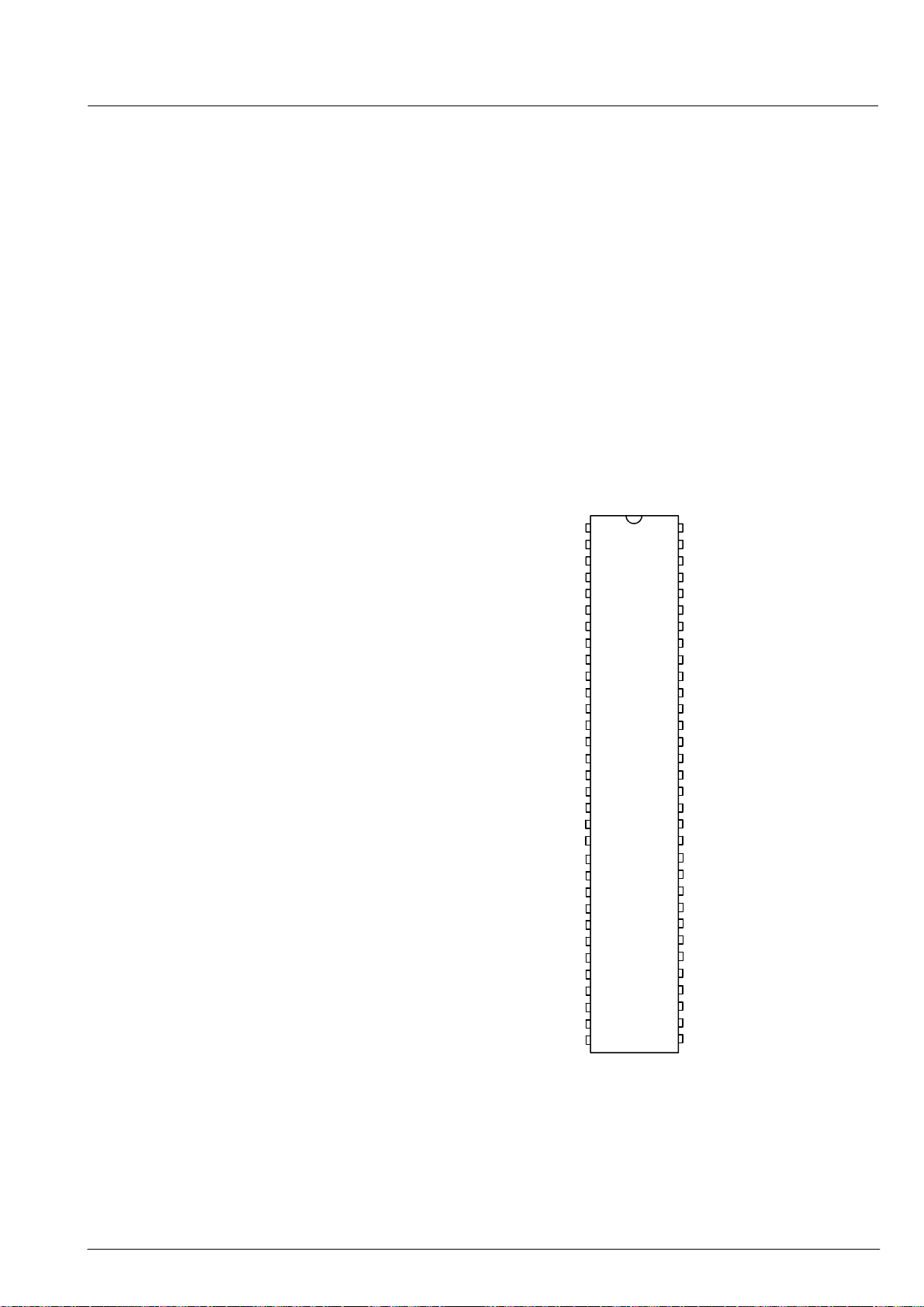
PRELIMINARY DATA SHEET VDP 31xxB
Pin 41, 42, 43, 45, 46, 47 – Analog RGB Inputs, RIN1/2,
GIN1/2, BIN1/2 (Fig. 4–15)
These pins are used to insert an external analog RGB
signal, e.g. from a SCART connector which can by
switched to the analog RGB outputs with the fast blank
signal. The analog backend provides separate brightness and contrast settings for the external analog RGB
signals.
Pin 44, 48 – Fast Blank Inputs, FBLIN1/2 (Fig. 4–15)
These pins are used to switch the RGB outputs to the external analog RGB inputs.
Pin 49 – Main Clock Output, CLK20 (Fig. 4–4)
This is the 20.25MHz main system clock, that is used by
all circuits in a high-end VDP system. All external timing
is derived from this clock.
Pin 50 – Horizontal Drive Output, HOUT (Fig. 4–18)
This open drain output supplies the the drive pulse for
the horizontal output stage. The polarity and gating with
the flyback pulse are selectable by software.
Pin 51, 52 – Crystal Input and Output, XTAL1, XTAL2
(Fig. 4–7)
These pins are connected to an 20.25 MHz crystal oscillator is digitally tuned by integrated shunt capacitances.
The Clk20 and Clk5 clock signals are derived from this
oscillator. An external clock can be fed into XTAL1. In
this case clock frequency adjustment must be switched
off.
Pin 53 – Standby Supply Voltage, VSTBY
In standby mode, only the clock oscillator and the horizontal drive circuitry are active.
Pin 54 – CCU 5 MHz Clock Output, CLK5 (Fig. 4–10)
This pin provides a clock frequency for the TV microcontroller, e.g. a CCU3000 controller.
Pin 55 – Ground (Analog Front-end), GND
F
Pin 56 – Ground (Analog Signal Input), ISGND (Fig. 4–8)
This is the high quality ground reference for the video
input signals.
Pin 57 – Reference Voltage Top, VRT (Fig. 4–8)
Via this pin, the reference voltage for the A/D converters
is decoupled. The pin is connected with 10 mF/47 nF to
the Signal Ground Pin.
Pin 59 – Analog Video Output, VOUT (Fig. 4–6)
The analog video signal that is selected for the main
(luma, cvbs) adc is output at this pin. An emitter follower
is required at this pin.
Pin 60 – Analog Chroma Input, CIN (Fig. 4–9)
This pin is connected to the S-VHS chroma signal. A re-
sistive divider is used to bias the input signal to the
middle of the converter input range. CIN can only be
connected to the chroma (Video 2) A/D converter. The
signal must be AC-coupled.
Pin 61...64 – Analog Video Input 1–4, VIN1–4 (Fig. 4–11)
These are the analog video inputs. A CVBS or S-VHS
luma signal is converted using the luma (Video 1) AD
converter. The input signal must be AC-coupled.
4.4. Pin Configuration
1
TEST
2
RESQ
3
SCL
SDA
4
CSY
MSY
INTLC
HFLB
PR0
PR1
PR2
RSW2
RSW1
GNDM
GNDV
VERT
EW
5
6
7
8
9
10
11
12
13
14
15
16
17
18
19
20
21
22
23
24
25
26
27
28
29
30
31
32
DSGND
PORT0/HCS
PORT1/FSY
VPROT
SAFETY
GNDDF
VSUPD
GNDDO
COLOR4/PORT2 RIN2
COLOR3/PORT3
COLOR2/PORT4
COLOR1/PORT5
COLOR0/PORT6
DSGND
SENSE
64
63
62
61
60
59
58
57
56
55
54
53
52
51
50
49
48
47
46
VDP 31xxB
45
44
43
42
41
40
39
38
37
36
35
34
33
VIN4
VIN3
VIN2
VIN1
CIN
VOUT
VSUPF
VRT
ISGND
GNDF
CLK5
VSTBY
XTAL2
XTAL1
HOUT
CLK20
FBLIN2
BIN2
GIN2
FBLIN
BIN
GIN
RIN
VRD
BOUT
GOUT
ROUT
VSUPO
GNDO
SVMOUT
XREF
Pin 58 – Supply Voltage (Analog Front-end), VSUP
F
Fig. 4–2: 64-pin PSDIP package
51Micronas
Page 52
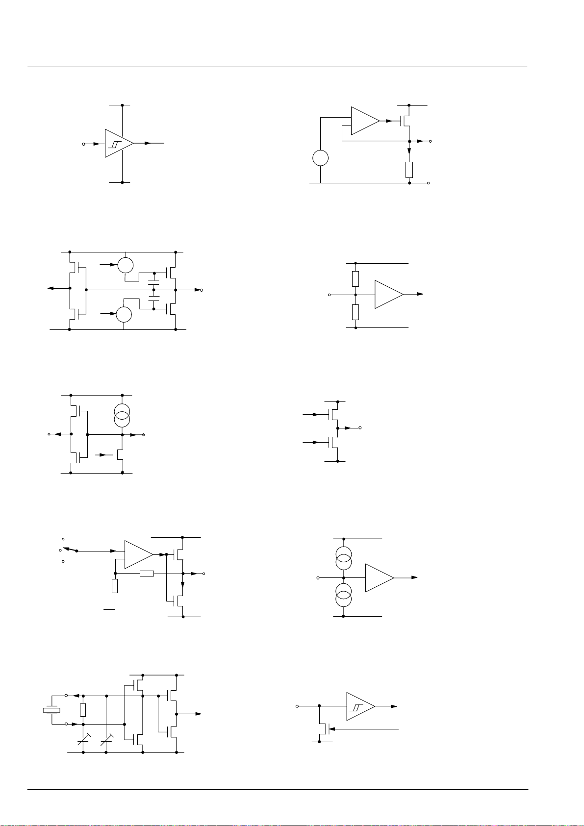
VDP 31xxB PRELIMINARY DATA SHEET
4.5. Pin Circuits
V
SUPD
GND
D
Fig. 4–3: Input pins RESQ, TEST
P
N
Fig. 4–4: Output pin CLK20
V
–
+
P
SUPF
VRT
Vref
ISGND
Fig. 4–8: Pins VRT , ISGND
V
SUPD
P
V
SUPF
To ADC
N
GND
GND
D
Fig. 4–9: Chroma input CIN
F
V
SUPD
P
N
N
GND
D
Fig. 4–5: Input/Output pins PR[2:0]
Vin’s
VREF
–
+
P
N
Fig. 4–6: Output pin VOUT
V
P
STBY
P
0.5M
f
ECLK
N
N
GND
Fig. 4–7: Input/Output pins XTAL1, XTAL2
V
SUPF
V
OUT
GND
F
VSTBY
P
N
GND
F
Fig. 4–10: Output pin CLK5
V
SUPF
To ADC
F
GND
F
Fig. 4–11: Input pins VIN1–VIN4
GND
D
Fig. 4–12: Pins SDA, SCL
52 Micronas
Page 53
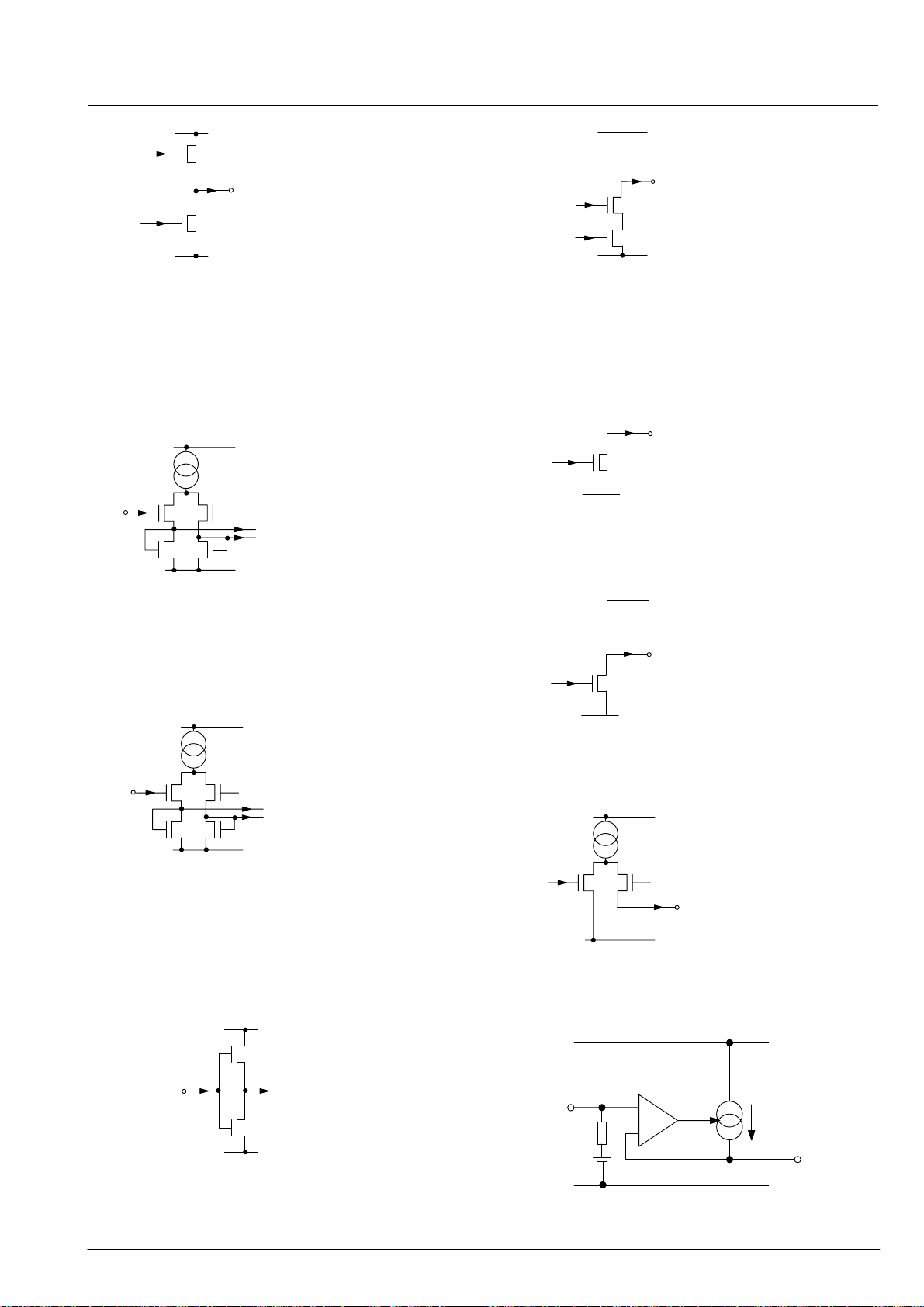
PRELIMINARY DATA SHEET VDP 31xxB
V
SUPD
P
N
GNDD
Fig. 4–13: Output pins FSY, MSY, CSY, INTLC,
PORT[6:0]
V
SUPD
PP
BIAS
NN
GNDD
V
SUPO
N
BIAS
N
GNDO
Fig. 4–17: Analog output pins ROUT, GOUT,
BOUT, SVMOUT
V
STDBY
N
GNDD
Fig. 4–18: Output pin HOUT
Fig. 4–14: Input pins SAFETY, VPROT, HFLB
V
SUPO
PP
BIAS
NN
GNDO
Fig. 4–15: Input pins FBLIN1/2, RIN1/2, BIN1/2,
GIN1/2, SENSE
V
SUPD
P
V
SUPO
N
GNDM
Fig. 4–19: Output pins RSW1, RSW2
V
SUPO
PP
GNDV
Fig. 4–20: Output pins VERT, EW
V
SUPO
N
GNDD
Fig. 4–16: Input pins COLOR[4:0], HCS,
PORT[6:0]
VRD
+
–
int. ref.
voltage
Fig. 4–21: Input pins XREF, VRD
ref. current
XREF
GNDO
53Micronas
Page 54
VDP 31xxB PRELIMINARY DATA SHEET
4.6. Electrical Characteristics
4.6.1. Absolute Maximum Ratings
Symbol Parameter Pin No. Min. Max. Unit
T
T
V
V
V
A
S
SUP
I
O
Ambient Operating Temperature – 0 65 °C
Storage Temperature – –40 125 °C
Supply Voltage, all Supply Inputs –0.3 6 V
Input Voltage, all Inputs –0.3 V
Output Voltage, all Outputs –0.3 V
+0.3 V
SUP
+0.3 V
SUP
Stresses beyond those listed in the “Absolute Maximum Ratings” may cause permanent damage to the device. This
is a stress rating only . Functional operation of the device at these or any other conditions beyond those indicated in the
“Recommended Operating Conditions/Characteristics” of this specification is not implied. Exposure to absolute maximum ratings conditions for extended periods may affect device reliability.
4.6.2. Recommended Operating Conditions
Symbol Parameter Pin Name Min. Typ. Max. Unit
T
V
A
SUP
Ambient Operating Temperature – 0 – 65 °C
Supply Voltages, all Supply Pins 4.75 5.0 5.25 V
f
XTAL
R
xref
Clock Frequency XTAL1/2 – 20.25 – MHz
RGB – DAC Current defining Re-
XREF 9.5 10 10.5
sistor
NS
VDD
Negative Slope of VDD (power
VSUPD 0.2 V/µs
down)
4.6.3. Recommended Crystal Characteristics
Symbol Parameter Min. Typ. Max. Unit
T
A
f
P
DfP/f
DfP/f
R
R
P
P
Operating Ambient Temperature 0 – 65 °C
Parallel Resonance Frequency
with Load Capacitance C
= 13 pF
L
– 20.250000 – MHz
Accuracy of Adjustment – – $20 ppm
Frequency Temperature Drift – – $30 ppm
Series Resistance – – 25
kW
W
C
0
C
1
Shunt Capacitance 3 – 7 pF
Motional Capacitance 20 – 30 fF
54 Micronas
Page 55
PRELIMINARY DATA SHEET VDP 31xxB
1)
g
0
Tuning condition: Code DVCO Register 720
Recommended Crystal Characteristics, continued
Symbol Parameter Min. Typ. Max. Unit
Load Capacitance Recommendation
C
Lext
External Load Capacitance 1)
– 3.3 – pF
from pins to Ground
(pin names: Xtal1 Xtal2)
DCO Characteristics
C
ICLoadmin
2)
Effective Load Capacitance @ min.
3.6 4.3 5 pF
DCO-Position, Code 0,
C
ICLoadrng
Effective Load Capacitance Range,
11.7 12.7 13.7 pF
DCO Codes from 0..255
Remarks on defining the External Load Capacitance:
External capacitors at each crystal pin to ground are required. They are necessary to tune the effective load capacitance of
the PCBs to the required load capacitance C
sults. The nominal free running frequency should match f
capacitor size should be determined in the application. The suggested value is a figure based on experience with various
PCB layouts.
condition: Code DVCO Register = –72
Tunin
2)
Remarks on Pulling Range of DCO:
The pulling range of the DCO is a function of the used crystal and effective load capacitance of the IC (C
The resulting frequency fL with an effective load capacitance of C
1 + 0.5 * [ C1 / (C0 + C
fL = fP * –––––––––––––––––––––––
1 + 0.5 * [ C1 / (C0 + CL ) ]
Leff
) ]
of the crystal. The higher the capacitors, the lower the clock frequency re-
L
MHz. Due to different layouts of customer PCBs the matching
p
+C
Leff
= C
ICLoad
+ C
LoadBoard
is
ICLoad
LoadBoard
).
4.6.4. Characteristics
= 0 to 65 °C, V
at T
at T
A
C
= 60 °C, V
SUPD/F/O
SUPD/F/O
= 5 V, f = 20.25 MHz for typical values
Symbol Parameter Pin Name Min. Typ. Max. Unit
I
VSUPF
I
VSUPD
I
VSUPO
I
VSTDBY
P
TOT
Current Consumption V
Current Consumption V
Current Consumption V
Current Consumption V
Total Power Dissipation – 1145 1200
IL Input / Output Leakage Current All I/O Pins –1 – 1
= 4.75 to 5.25 V, f = 20.25 MHz for min./max. values
SUPF
SUPD
SUPO
STDBY
– 38 – mA
– 123 – mA
– 64 – mA
– 3.3 – mA
W
mA
55Micronas
Page 56
VDP 31xxB PRELIMINARY DATA SHEET
TEST
4.6.4.1. 5 MHz Clock Output
Symbol Parameter Pin Name Min. Typ. Max. Unit Test Conditions
V
OL
V
OH
t
OT
Output Low Voltage CLK5 – – 0.4 V IOL = 0.4 mA
Output High Voltage 4.0 – VSTDBY V –IOL = 0.9 mA
Output Transition Time – 50 – ns C
LOAD
= 30 pF
4.6.4.2. 20 MHz Clock Input/Output, External Clock Input (XTAL1) (see Fig. 4–22)
Symbol Parameter Pin Name Min. Typ. Max. Unit Test Conditions
V
V
t
OT
V
f
F
V
V
DCAV
PP
IT
F
MIDC
F
MIAC
DC Average CLK20 V
V
Peak to Peak 1.3 1.6 – V C
OUT
Output Transition Time – – 18 ns C
SUP
– 0.3
/2
V
SUP
/2 V
SUP/
+ 0.3
2
V C
LOAD
LOAD
LOAD
= 30 pF
= 30 pF
= 30 pF
Input Trigger Level 2.1 2.5 2.9 V only for test purposes
FMain Clock Frequency
FMain Clock Input DC Voltage
FM Clock Input AC Voltage
XTAL 1 10 20.25 24 MHz
1.0 – 3.5 V
0.8 – 2.5 V
(p–p)
t
F
MIH
t
F
MIL
t
F
MIHL
t
F
MILH
FM Clock Input High/Low Ratio
FM Clock Input High to Low
Transition Time
FM Clock Input Low to High
Transition Time
t
F
MILH
V
F
MIAC
t
F
MIHL
0.9 1.0 1.1
– – 0.15
f
F
– – 0.15
f
F
t
F
MIH
M
M
t
F
MI
L
V
F
MIDC
0 V
DVSS
Fig. 4–22: Main clock input
4.6.4.3. Reset Input, Test Input
Symbol Parameter Pin Name Min. Typ. Max. Unit Test Conditions
V
IL
V
IH
56 Micronas
Input Low Voltage RESQ
Input High Voltage
– – 1.5 V
3.0 – – V
Page 57
PRELIMINARY DATA SHEET VDP 31xxB
4.6.4.4. I2C Bus Interface
Symbol Parameter Pin Name Min. Typ. Max. Unit Test Conditions
V
IL
V
IH
V
OL
V
IH
t
F
t
R
f
SCL
t
LOW
t
HIGH
t
SU Data
t
HD Data
Input Low Voltage SDA, SCL – – 1.5 V
Input High Voltage 3.0 – – V
Output Low Voltage – – 0.4
Input Capacitance – – 4 pF
Signal Fall Time – – 300 ns CL = 400 pF
Signal Rise Time – – 300 ns CL = 400 pF
Clock Frequency SCL 0 – 400 kHz
Low Period of SCL 1.3 – –
High Period of SCL 0.6 – –
Data Set Up Time to SCL high SDA 100 – – ns
DATA Hold Time to SCL low 0 – 0.9
4.6.4.5. IO Port Expander
0.6
V
V
ms
ms
ms
Il = 3 mA
I
= 6 mA
l
Symbol Parameter Pin Name Min. Typ. Max. Unit Test Conditions
V
IL
V
IH
V
OL
V
OH
t
OD
I
OL
Input Low Voltage PORT[6:0] – – 0.8 V
Input High Voltage 1.5 – – V
Output Low Voltage – 0.2 0.4 V IOL = 1.6 mA,
strength 6
Output High Voltage V
SUPD
– 0.4
Output Transition Time – – 35 ns C
– V
SUPD
V –IOL = 1.6mA,
strength 6
= 70pF
LOAD
Output Current –10 – 10 mA driver imp. = 0
4.6.4.6. Analog Video Inputs
Symbol Parameter Pin Name Min. Typ. Max. Unit Test Conditions
V
VIN
Analog Input Voltage VIN1
VIN2
VIN3
VIN4
CIN
0 – 3.5 V
C
CP
Input Coupling Capacitor
Video Inputs
VIN1
VIN2
– 680 – nF
VIN3
VIN4
C
CP
Input Coupling Capacitor
Chroma Input
CIN – 1 – nF
57Micronas
Page 58
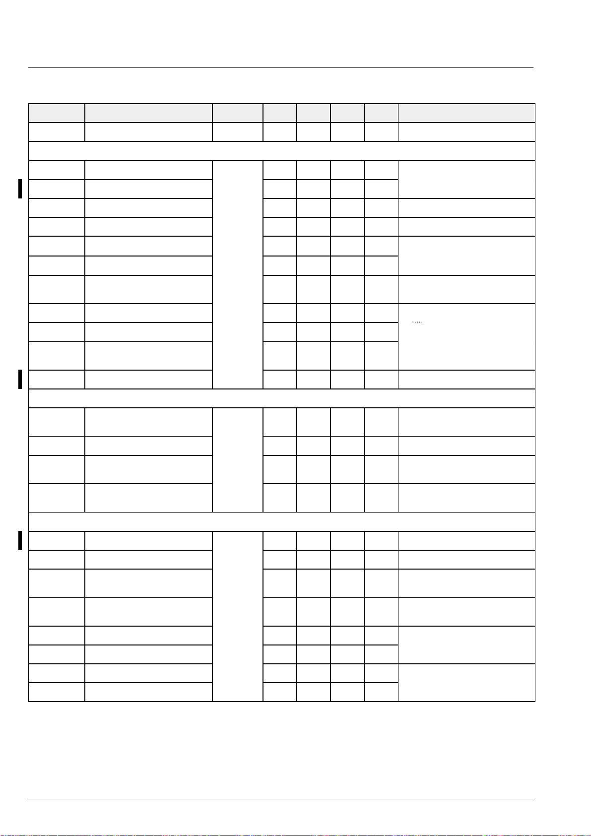
VDP 31xxB PRELIMINARY DATA SHEET
VIN2
VIN4
f
MHz
V
V
VIN2
VIN4
DC-ramp
ramp
4.6.4.7. Analog Front-End and ADCs
Symbol Parameter Pin Name Min. Typ. Max. Unit Test Conditions
V
VRT
Reference Voltage Top VRT 2.5 2.6 2.8 V
10 mF/10 nF, 1 GW Probe
Luma – Path
R
VIN
C
VIN
V
VIN
V
VIN
Input Resistance VIN1
Input Capacitance
VIN3
Full Scale Input Voltage
1
4.5 pF
1.8 2.0 2.2 V
Full Scale Input Voltage 0.5 0.6 0.7 V
MW
Code Clamp – DAC = 0
min. AGC Gain
PP
max. AGC Gain
PP
AGC AGC Step Width 0.166 dB 6-Bit Resolution = 64 Steps
= 1
= 1.5
,
DNL
V
VINCL
Q
CL
I
CL–LSB
DNL
C
ICL
AGC
ICL
sig
AGC Differential Non-Linearity ±0.5 LSB
–2 dBr of max. AGC-Gain
Input Clamping Level, CVBS 1.0 V Binary Level = 64 LSB
min. AGC Gain
Clamping DAC Resolution –16 15 steps 5 Bit – I-DAC, bipolar
Input Clamping Current per Step 0.7 1.0 1.3
Clamping DAC Differential Non-
±0.5 LSB
mA
VIN
Linearity
Clamping-Capacity 220 – nF Coupling-Cap. @ Inputs
Chroma – Path
R
CIN
Input Resistance
SVHS Chroma
CIN
VIN1
1.4 2.0 2.6
kW
V
CIN
V
CINDC
Full Scale Input Voltage, Chroma 1.08 1.2 1.32 V
Input Bias Level,
– 1.5 – V
SVHS Chroma
Binary Code for Open
128
PP
Chroma Input
Dynamic Characteristics for all Video Paths (Luma + Chroma)
BW Bandwidth VIN1
XTALK Crosstalk, any Two Video Inputs
THD Total Harmonic Distortion
VIN3
CIN
10 12.5 MHz –2 dBr input signal level
–56 dB 1 MHz, –2 dBr signal level
50 dB 1 MHz, 5 harmonics,
–2 dBr signal level
SINAD Signal to Noise and Distortion
Ratio
45 dB 1 MHz, all outputs,
–2 dBr signal level
INL Integral Non-Linearity, ±1 LSB Code Density,
p
DNL Differential Non-Linearity ±0.8 LSB
DG Differential Gain ±3 % –12 dBr, 4.4 MHz signal on DC-
p
DP Differential Phase 1.5 deg
58 Micronas
Page 59
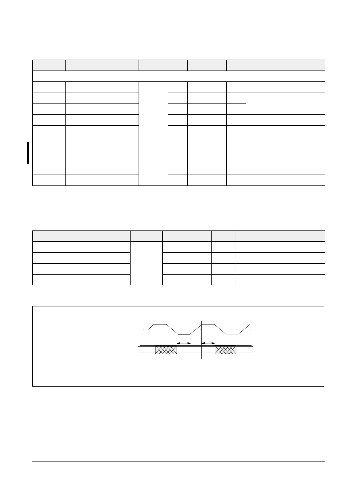
PRELIMINARY DATA SHEET VDP 31xxB
3 MSB’s of main AGC
COL
Analog Front-End and ADCs, continued
Symbol Parameter Pin Name Min. Typ. Max. Unit Test Conditions
Analog Video Output
V
OUT
AGC
VOUT
DNL
AGC
V
OUTDC
BW V
THD V
C
LVOUT
I
LVOUT
Output Voltage VOUT 1.7 2.0 2.3 V
PP
AGC Step Width, VOUT 1.333 dB 3 Bit Resolution = 7 Steps
AGC Differential Non-Linearity ±0.5 LSB
DC-Level 1 V clamped to back porch
Bandwidth 10 MHz Input: –2 dBr of main ADC range,
OUT
T otal Harmonic Distortion –45 –40 dB Input: –2 dBr of main ADC range,
OUT
Load Capacitance – – 10 pF
Output Current – – ±0.1 mA
V
= 1 VPP, AGC = 0 dB
VIN
’
C
≤ 10 pF
L
C
≤ 10 pF
L
1 MHz, 5 Harmonics
4.6.4.8. Picture Bus Input (see Fig. 4–23)
Symbol Parameter Pin Name Min. Typ. Max. Unit Test Conditions
V
IL
V
IH
Input Low Voltage PR[2:0]
-
Input High Voltage
OR[4:0]
– – 0.8 V
1.5 – – V
t
IS
t
IH
Input Setup Time 7 – – ns
Input Hold Time 5 – – ns
Main Clock
t
IS
t
IH
Data Inputs
Fig. 4–23: Picture bus input timing
59Micronas
Page 60
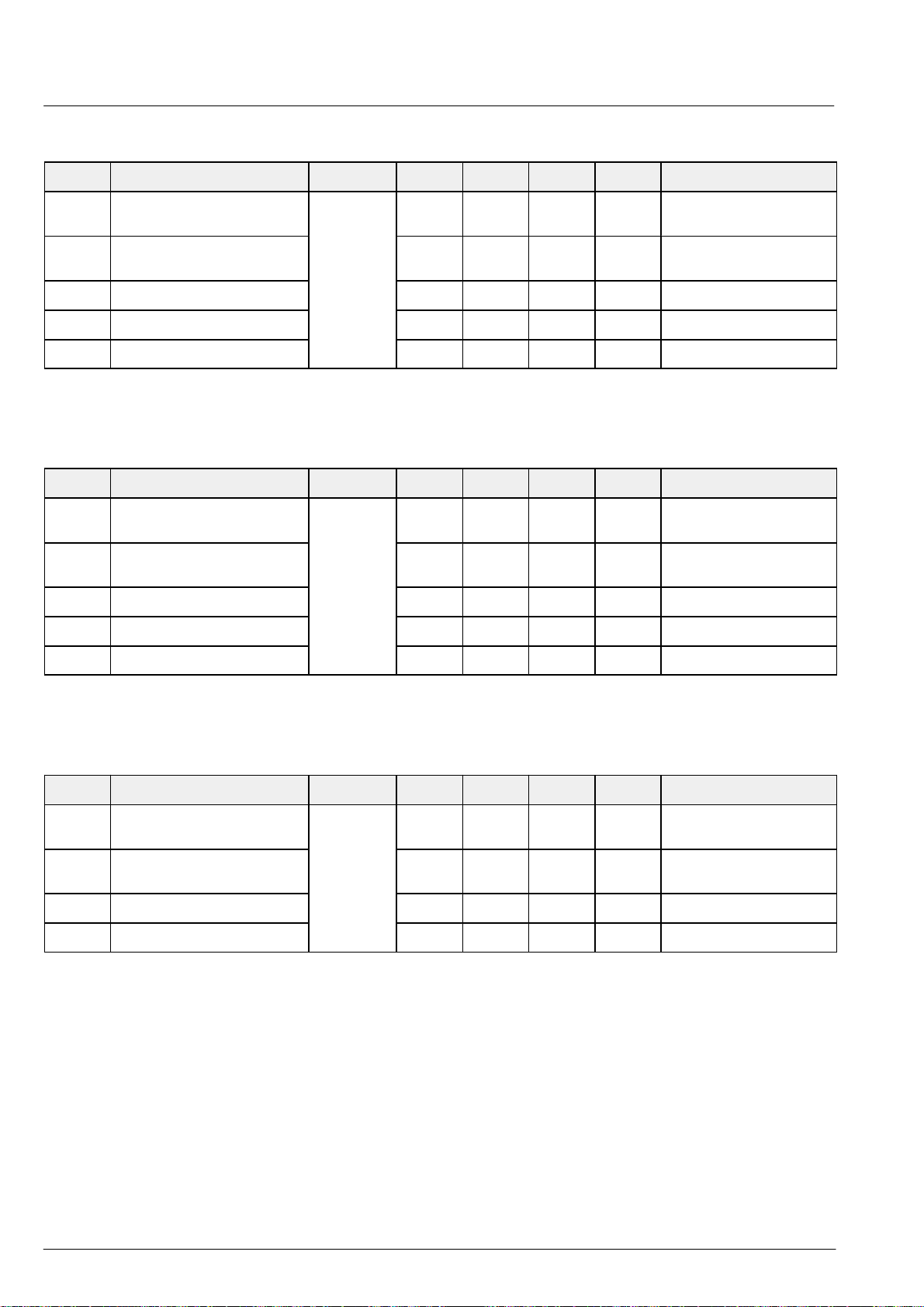
VDP 31xxB PRELIMINARY DATA SHEET
4.6.4.9. INTLC, Front Sync Output
Symbol Parameter Pin Name Min. Typ. Max. Unit Test Conditions
V
OL
V
OH
t
OH
t
OD
I
OL
Output Low Voltage INTLC
FSY
Output High Voltage V
Output Hold Time 6 14 ns C
Output Delay Time – – 35 ns C
– 0.2 0.4 V IOL = 1.6 mA,
strength 6
SUPD
– 0.4
– V
SUPD
V –IOL = 1.6mA,
strength 6
= 70pF
LOAD
= 70pF
LOAD
Output Current –10 – 10 mA driver imp. = 0
4.6.4.10. Main Sync Output
Symbol Parameter Pin Name Min. Typ. Max. Unit Test Conditions
V
OL
V
OH
t
OH
t
OD
Output Low Voltage MSY – 0.2 0.4 V IOL = 1.6 mA,
strength 6
Output High Voltage V
SUPD
– 0.4
Output Hold Time 6 14 ns C
Output Delay Time – – 35 ns C
– V
SUPD
V –IOL = 1.6mA,
strength 6
= 70pF
LOAD
= 70pF
LOAD
I
OL
Output Current –10 – 10 mA driver imp. = 0
4.6.4.11. Combined Sync Output
Symbol Parameter Pin Name Min. Typ. Max. Unit Test Conditions
V
OL
V
OH
t
OT
I
OL
Output Low Voltage CSY – – 0.4 V IOL = 1.6 mA
strength 6
Output High Voltage V
SUPD
– 0.4
Output Transition Time – 10 20 ns C
– V
SUPD
V –IOL = 1.6 mA
strength 6
= 30 pF
LOAD
Output Current –10 – 10 mA driver imp. = 0
60 Micronas
Page 61
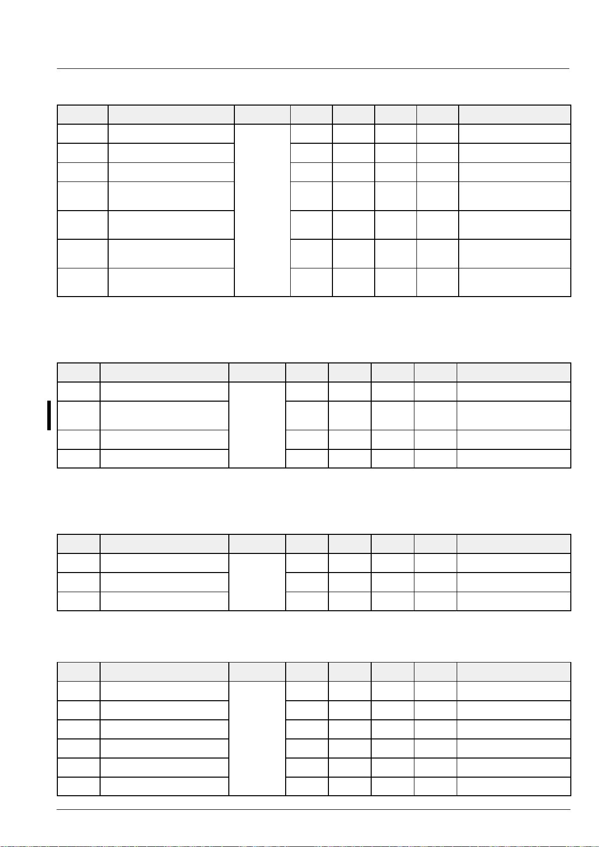
PRELIMINARY DATA SHEET VDP 31xxB
4.6.4.12. Horizontal Flyback Input
Symbol Parameter Pin Name Min. Typ. Max. Unit Test Conditions
V
IL
V
IH
V
IHST
PSRR
PSRR
PSRR
t
PID
Input Low Voltage HFLB – – 1.8 V
Input High Voltage 2.6 – – V
Input Hysteresis 0.1 – – V
Power Supply Rejection Ratio of
HF
Trigger Level
Power Supply Rejection Ratio of
MF
Trigger Level
Power Supply Rejection Ratio of
LF
Trigger Level
0 dB f = 20 MHz
–20 dB f < 15 kHz
–40 dB f < 100 Hz
Internal Delay 12 ns slew rate 500 mV/ns
swing 1 V
4.6.4.13. Horizontal Drive Output
Symbol Parameter Pin Name Min. Typ. Max. Unit Test Conditions
V
OL
V
OH
Output Low Voltage HOUT – – 0.4 V IOL = 10 mA
Output High Voltage
– – 5 V external pull-up resistor
(Open Drain Stage)
PP
t
OF
I
OL
Output Fall Time – 8 20 ns C
Output Low Current – – 10 mA
LOAD
= 30pF
4.6.4.14. Vertical Protection Input
Symbol Parameter Pin Name Min. Typ. Max. Unit Test Conditions
V
V
V
IL
IH
IHST
Input Low Voltage VPROT – – 1.8 V
Input High Voltage 2.6 – – V
Input Hysteresis 0.1 – – V
4.6.4.15. Vertical Safety Input
Symbol Parameter Pin Name Min. Typ. Max. Unit Test Conditions
V
ILA
V
IHA
V
ILB
Input Low Voltage A SAFETY – – 1.8 V
Input High Voltage A 2.6 – – V
Input Low Voltage B – – 3.1 V
V
V
t
PID
IHB
IHST
Input High Voltage B 3.9 – – V
Input Hysteresis A and B 0.1 – – V
Internal Delay 100 ns
61Micronas
Page 62
VDP 31xxB PRELIMINARY DATA SHEET
RSW2
BIN
BIN2
4.6.4.16. Vertical and East
/West Drive Output
Symbol Parameter Pin Name Min. Typ. Max. Unit Test Conditions
V
V
I
dacn
OL
OH
Output Voltage LOW EW
Output Voltage HIGH 2.82 3 3.2 V R
Full scale DAC Output
Current
PSRR Power Supply Rejection
VERT
0 V R
415 440 465 µA Vo = 0 V
20 – – dB
R
R
R
load
xref
load
xref
xref
= 6800
= 10 kW
= 6800
= 10 kW
= 10 kW
Ratio
4.6.4.17. Sense A/D Converter Input
Symbol Parameter Pin Name Min. Typ. Max. Unit Test Conditions
V
I
V
I255
Input Voltage Range SENSE 0 – V
sup
V
Input Voltage for code 255 1.4 1.54 1.7 V Read cutoff blue
register
C
0
Digital Output for zero Input 16 LSB Offset check,
read cutoff blue
register
R
I
Input Impedance 1 – –
MW
Range Switch Outputs
R
ON
I
Max
I
LEAK
C
IN
Output On Resistance RSW1
Maximum Current
– – 50
W
– – 15 mA
Leakage Current – – 600 nA RSW High Impedance
Input Capacitance – – 4 pF
I
OL
= 10 mA
4.6.4.18. Analog RGB and FB Inputs (continued on next page)
Symbol Parameter Pin Name Min. Typ. Max. Unit T est Conditions
V
RGBIN
V
RGBIN
External RGB Inputs Voltage
Range
nominal RGB Input Voltage
peak-to-peak
RIN
GIN
RIN2
GIN2
–0.3 – 1.1 V
0.5 0.7 1.0 V
PP
SCART Spec: 0.7 V ±3 dB
V
RGBIN
RGB Inputs Voltage for Maximum Output Current
RGB Inputs Voltage for Maxi-
0.44 Contrast setting: 51 1
0.7 Contrast setting: 323
mum Output Current
RGB Inputs Voltage for Maxi-
1.1 Contrast setting: 204
mum Output Current
62 Micronas
Page 63
PRELIMINARY DATA SHEET VDP 31xxB
BIN
GIN2
FBLIN2
Analog RGB and FB Inputs, continued
Symbol Parameter Pin Name Min. Typ. Max. Unit T est Conditions
C
RGBIN
C
IN
I
IL
V
CLIP
V
CLAMP
V
INOFF
V
INOFF
R
CLAMP
V
FBLOFF
V
FBLON
V
FBLTRIG
External RGB Input Coupling
Capacitor
Clamp Pulse Width
Input Capacitance
Input Leakage Current –0.5 – 0.5
RGB Input Voltage for
RIN
GIN
RIN2
BIN2
15 nF
3.1 µs
– – 13 pF
mA
2 V
Clamping OFF,
V
–0.3..3 V
IN
Clipping Current
Clamp Level at Input 40 60 80 mV Clamping ON
Offset Level at Input –10 10 mV Extrapolated from
V
= 100 mV
IN
and 200 mV
Offset Level Match at Input –10 10 mV Extrapolated from
V
= 100 mV and 200 mV
IN
Clamping-ON-Resistance 140 – Ω
FBLIN Low Level FBLIN
FBLIN High Level
Fast Blanking Trigger
– – 0.5 V
0.9 – – V
0.7
Level typical
t
PID
Delay Fast Blanking to RGB
from midst of FBLIN-transition
to 90% of RGB
-transition
OUT
OUT
8 15 ns Internal RGB = 3.75 mA Full
Scale
Int. Brightness = 0
External Brightness =
1.5 mA (Full Scale)
RGBin = 0
Difference of Internal Delay to
V
V
Rise and fall time = 2 ns
–5 +5 ns
FBLOFF
FBLON
= 0.4 V
= 1.0 V
External RGBin Delay
Switch-Over-Glitch 0.5 pAs Switch from 3.75 mA (int) to
1.5 mA (ext)
4.6.4.19. Half Contrast Switch Input
Symbol Parameter Pin Name Min. Typ. Max. Unit Test Conditions
V
V
t
HCS
IL
IH
Input Low Voltage HCS – – 0.8 V
Input High Voltage 1.5 – – V
Delay HCS to RGB
from 50% of HCS-transition
to 90% of RGB
-transition
OUT
OUT
80 120 ns Internal RGB = 3.75 mA
V
= 0.4 V
HCSL
V
= 1.0 V
HCSH
Rise and fall time = 2 ns
63Micronas
Page 64
VDP 31xxB PRELIMINARY DATA SHEET
GOUT
3.75 mA
GOUT
GOUT
4.6.4.20. Analog RGB Outputs, D/A Converters
Symbol Parameter Pin Name Min. Typ. Max. Unit Test Conditions
Internal RGB Signal D/A Converter Characteristics
I
OUT
I
OUTHC
t
T
t
RHC
t
FHC
D
RGB
D
RGBHC
Resolution ROUT
Full Scale Output Current
BOUT
Half Contrast Output Current 1.74 1.87 2.0 mA R
– 10 – bit
3.6 3.75 3.9 mA R
I
OUT
ref
ref
= 10 kΩ
= 10 kΩ,
= 3.75 mA
Differential Nonlinearity 0.5 LSB
Integral Nonlinearity 1 LSB
Glitch Pulse Charge 0.5 pAs Ramp signal, 25 Ω output ter-
mination
Rise and Fall Time 3 ns 10% to 90%, 90% to 10%
Half Contrast Rise Time 50 75 ns 60% to 90% I
Half Contrast Fall Time 25 40 ns 90% to 60% I
= 3.75mA
OUT
= 3.75mA
OUT
Intermodulation –50 dB 2/2.5 MHz full scale
Signal to Noise +50 dB Signal: 1MHz full scale
Bandwidth: 10MHz
Matching R–G, R–B, G–B –2 2 %
Half Contrast Matching
–5 5 %
R–G, R–B, G–B
R/B/G Crosstalk
one channel talks
two channels talk
RGB Input Crosstalk from
–46 dB Passive channel:
I
=1.88 mA
OUT
Crosstalk-Signal: 1.25 MHz,
PP
external RGB
one channel talks
two channels talk
three channels talk
–50
–50
–50
dB
dB
dB
Internal RGB Brightness D/A Converter Characteristics
Resolution ROUT
I
BR
I
BR
I
BR
I
BR
I
BR
I
BR
Full Scale Output Current
relative
Full Scale Output Current
absolute
differential nonlinearity 0.5 LSB
integral nonlinearity 1 LSB
Match R–G, R–B, G–B –2 2 %
Match to digital RGB
R–R, G–G, B–B
External RGB Voltage/Current Converter Characteristics
Resolution ROUT
I
EXOUT
Full Scale Output Current
relative
Full Scale Output Current
absolute
BOUT
BOUT
9 bits
39.2 40 40.8 % Ref to max. digital RGB
1.5 mA
–2 2 %
9 bits
96 100 104 % Ref. to max. Digital RGB
V
= 0.7 VPP, contrast = 323
IN
3.75 mA Same as Digital RGB
64 Micronas
Page 65
PRELIMINARY DATA SHEET VDP 31xxB
GOUT
GOUT
Analog RGB Outputs, D/A Converters, continued
Symbol Parameter Pin Name Min. Typ. Max. Unit Test Conditions
CR Contrast Adjust Range ROUT
Gain Match R–G, R–B, G–B
BOUT
Gain Match to RGB–DACs
R–R, G–G, B–B
R/B/G Input Crosstalk
one channel talks
two channels talk
RGB Input Crosstalk from
Internal RGB
one channel talks
two channels talk
three channels talk
RGB Input Noise and
Distortion
RGB Input Bandwidth –3dB 10 15 – MHz VIN = 0.7 VPP,
RGB Input THD –50
Differential Nonlinearity of
Contrast Adjust
16:511
–2 2 % Measured at RGB Outputs
V
= 0.7 V, contrast = 323
IN
–3 3 % Measured at RGB Outputs
V
= 0.7 V, contrast = 323
IN
–46 dB Passive channel:
V
= 0.7V,
IN
contrast = 323
–50 dB
–50 dB V
Crosstalk signal: 1.25 MHz,
3.75 mA
PP
= 0.7 VPP at 1 MHz
IN
contrast = 323
Bandwidth: 10 MHz
contrast = 323
–40
dB
dB
Input signal 1 MHz
Input signal 6 MHz
V
= 0.7 V
IN
contrast = 323
PP
1.0 LSB VIN = 0.44 V
Integral nonlinearity of
Contrast Adjust
V
RGBO
RGB Output Voltage –1.0 0.3 V Referred to V
RGB Output Load Resistance 100 Ω Ref. to V
V
OUTC
RGB Output Compliance –1.5 –1.3 –1.2 V Ref. to V
External RGB Brightness D/A Converter Characteristics
Resolution ROUT
I
EXBR
Full Scale Output Current
relative
BOUT
Full Scale Output Current
absolute
Differential Nonlinearity 0.5 LSB
Integral Nonlinearity 1 LSB
Matching R–G, R–B, G–B –2 2 %
Matching to digital RGB
R–R, G–G, B–B
7 LSB
SUPO
SUPO
Sum of max. Current of
SUPO
RGB–DACs and max. Current of Int. Brightness DACs
is 2% degraded
9 bits
39.2 40 40.8 % Ref to max. digital RGB
1.5 mA
–2 2 %
65Micronas
Page 66
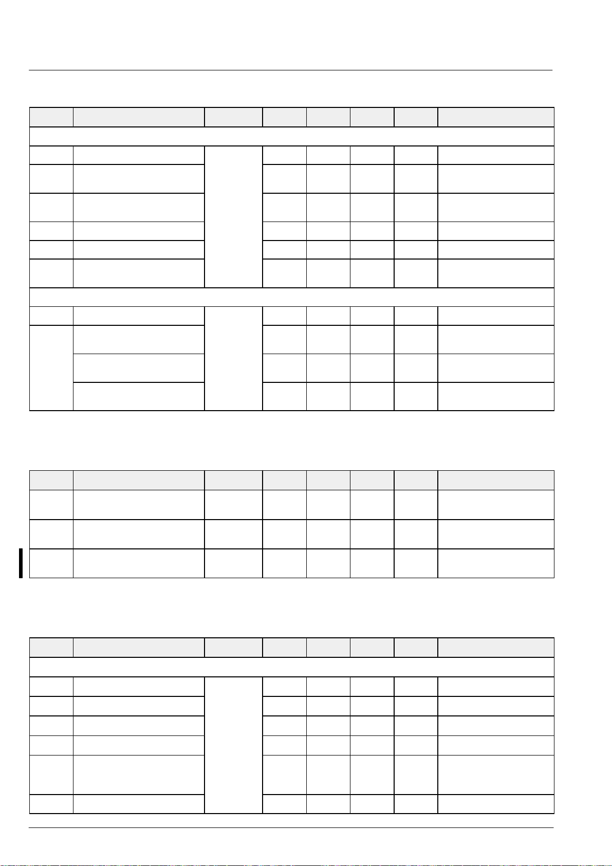
VDP 31xxB PRELIMINARY DATA SHEET
GOUT
GOUT
Analog RGB Outputs, D/A Converters, continued
Symbol Parameter Pin Name Min. Typ. Max. Unit Test Conditions
RGB Output Cutoff D/A Converter Characteristics
Resolution ROUT
I
CUT
I
CUT
I
CUT
I
CUT
I
CUT
Full Scale Output Current
BOUT
relative
Full Scale Output Current
absolute
Differential nonlinearity 0.5 LSB
Integral nonlinearity 1 LSB
Match to digital RGB
R–R, G–G, B–B
RGB Output Ultrablack D/A Converter Characteristics
Resolution ROUT
I
UB
Full Scale Output Current
relative
BOUT
Full Scale Output Current
absolute
Match to digital RGB
R–R, G–G, B–B
4.6.4.21. DAC Reference, Beam Current Safety
9 bits
58.8 60 61.2 % Ref to max. digital RGB
2.25 mA
–2 2 %
1 bits
19.6 20 20.4 % Ref to max. digital RGB
0.75 mA
*2 2 %
Symbol Parameter Pin Name Min. Typ. Max. Unit Test Conditions
V
DACREF
DAC-Reference Voltage VRD/BCS 2.38 2.50 2.67 V
DAC-Reference Output
VRD/BCS 18 25 32
kW
resistance
V
XREF
DAC-Reference Voltage
Bias Current Generation
XREF 2.25 2.34 2.43 V R
= 10 kΩ,
ref
4.6.4.22. Scan Velocity Modulation Output
Symbol Parameter Pin Name Min. Typ. Max. Unit Test Conditions
SVM D/A Converter Characteristics
Resolution SVMOUT 8 bit
I
OUT
I
OUT
I
OUT
I
OUT
Full Scale Output Current 1.55 1.875 2.25 mA
Differential Nonlinearity 0.5 LSB
Integral Nonlinearity 1 LSB
Glitch Pulse Charge 0.5 pAs Ramp, output line is
terminated on both ends with
50 Ohms
I
OUT
66 Micronas
Rise and Fall Time 3 nsec 10% to 90%, 90% to 10%
Page 67
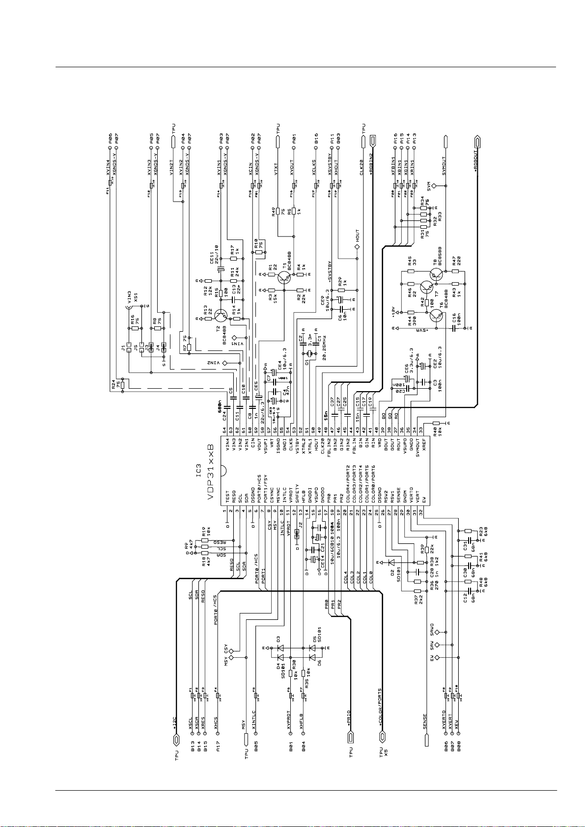
PRELIMINARY DATA SHEET VDP 31xxB
5. Application Circuit
67Micronas
Page 68
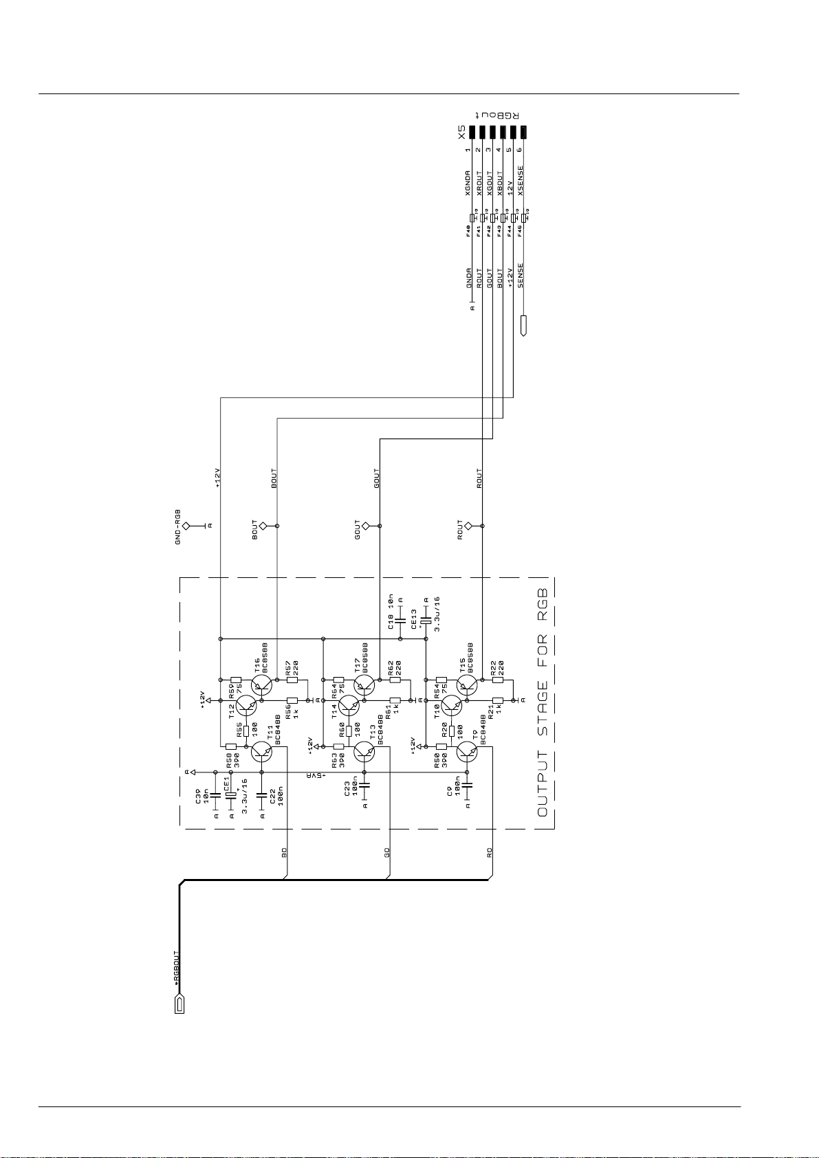
VDP 31xxB PRELIMINARY DATA SHEET
68 Micronas
Page 69

PRELIMINARY DATA SHEET VDP 31xxB
69Micronas
Page 70

VDP 31xxB PRELIMINARY DATA SHEET
70 Micronas
Page 71

PRELIMINARY DATA SHEET VDP 31xxB
71Micronas
Page 72

VDP 31xxB PRELIMINARY DATA SHEET
6. Data Sheet History
1. Preliminary data sheet: “VDP 31xxB Video Processor Family”, Edition May 15, 1997, 6251-437-1PD.
First release of the preliminary data sheet.
2. Preliminary data sheet: “VDP 31xxB Video Processor Family”, Edition Sept. 25, 1998, 6251-437-2PD.
Second release of the preliminary data sheet.
Major changes:
– section 4.1.: package outline dimensions changed
– section 4.6.: missing values have been defined
– section 5.: application circuit diagram corrected
Micronas GmbH
Hans-Bunte-Strasse 19
D-79108 Freiburg (Germany)
P.O. Box 840
D-79008 Freiburg (Germany)
Tel. +49-761-517-0
Fax +49-761-517-2174
E-mail: [email protected]
Internet: www.micronas.com
Printed in Germany
Order No. 6251-437-2PD
All information and data contained in this data sheet are without any
commitment, are not to be considered as an offer for conclusion of a
contract, nor shall they be construed as to create any liability . Any new
issue of this data sheet invalidates previous issues. Product availability
and delivery are exclusively subject to our respective order confirmation form; the same applies to orders based on development samples
delivered. By this publication, Micronas GmbH does not assume responsibility for patent infringements or other rights of third parties
which may result from its use.
Further, Micronas GmbH reserves the right to revise this publication
and to make changes to its content, at any time, without obligation to
notify any person or entity of such revisions or changes.
No part of this publication may be reproduced, photocopied, stored on
a retrieval system, or transmitted without the express written consent
of Micronas GmbH.
72 Micronas
 Loading...