

Page 1
VCT 38xxA
Video/Controller/Teletext
IC Family
Edition Oct. 17, 2000
6251-518-1AI
ADVANCE INFORMATION
MICRONAS
MICRONAS
Page 2

VCT 38xxA ADVANCE INFORMATION
Contents
Page Section Title
7 1. Introduction
81.1.Features
8 1.1.1. Video Features
8 1.1.2. Microcontroller Features
8 1.1.3. OSD Features
8 1.1.4. Teletext Features
8 1.1.5. Audio Features
8 1.1.6. General Features
9 1.2. Chip Architecture
10 1.3. System Application
11 2. Video Processing
11 2.1. Introduction
11 2.2. Video Front-end
11 2.2.1. Input Selector
11 2.2.2. Clamping
11 2.2.3. Automatic Gain Control
11 2.2.4. Analog-to-Digital Converters
12 2.2.5. Digitally Controlled Clock Oscillator
12 2.2.6. Analog Video Output
12 2.3. Adaptive Comb Filter
13 2.4. Color Decoder
13 2.4.1. IF-Compensation
14 2.4.2. Demodulator
14 2.4.3. Chrominance Filter
14 2.4.4. Frequency Demodulator
14 2.4.5. Burst Detection / Saturation Control
14 2.4.6. Color Killer Operation
15 2.4.7. Automatic Standard Recognition
15 2.4.8. PAL Compensation/1-H Comb Filter
16 2.4.9. Luminance Notch Filter
16 2.4.10. Skew Filtering
16 2.5. Horizontal Scaler
16 2.6. Black-line Detector
17 2.7. Test Pattern Generator
17 2.8. Video Sync Processing
18 2.9. Macrovision Detection
18 2.10. Display Processing
18 2.10.1. Luma Contrast Adjustment
18 2.10.2. Black-Level Expander
19 2.10.3. Dynamic Peaking
21 2.10.4. Digital Brightness Adjustment
21 2.10.5. Soft Limiter
21 2.10.6. Chroma Interpolation
21 2.10.7. Chroma Transient Improvement
22 2.10.8. Inverse Matrix
22 2.10.9. RGB Processing
22 2.10.10. OSD Color Look-up Table
22 2.10.11. Picture Frame Generator
23 2.10.12. Priority Decoder
23 2.10.13. Scan Velocity Modulation
23 2.10.14. Display Phase Shifter
2 Micronas
Page 3

ADVANCE INFORMATION
Contents, continued
Page Section Title
25 2.11. Video Back-end
25 2.11.1. CRT Measurement and Control
26 2.11.2. SCART Output Signal
27 2.11.3. Average Beam Current Limiter
27 2.11.4. Analog RGB Insertion
27 2.11.5. Fast-Blank Monitor
29 2.12. Synchronization and Deflection
29 2.12.1. Deflection Processing
29 2.12.2. Angle and Bow Correction
29 2.12.3. Horizontal Phase Adjustment
30 2.12.4. Vertical and East/West Deflection
30 2.12.5. EHT Compensation
31 2.12.6. Protection Circuitry
31 2.13. Reset Function
31 2.14. Standby and Power-On
2
32 2.15. I
32 2.15.1. Control and Status Registers
44 2.15.1.1. Scaler Adjustment
46 2.15.1.2. Calculation of Vertical and East-West Deflection Coefficients
C Bus Slave Interface
VCT 38xxA
47 3. Text and OSD Processing
47 3.1. Introduction
47 3.2. SRAM Interface
47 3.3. Text Controller
49 3.4. Teletext Acquisition
49 3.5. Teletext Page Management
49 3.5.1. Memory Manager
50 3.5.2. Memory Organization
50 3.5.3. Page Table
52 3.5.4. Ghost Row Organization
52 3.5.5. Subpage Manager
53 3.6. WST Display Controller
55 3.7. Display Memory
57 3.8. Character Generator
58 3.8.1. Character Code Mapping
59 3.8.2. Character Font ROM
60 3.8.3. Latin Font Mapping
61 3.8.4. Cyrillic Font Mapping
62 3.8.5. Arabic Font Mapping
63 3.8.6. Character Font Structure
64 3.9. National Character Mapping
66 3.10. Four-Color Mode
67 3.11. OSD Layer
68 3.12. Command Language
76 3.13. I/O Register
2
82 3.14. I
82 3.14.1. Subaddressing
82 3.14.1.1. CPU Subaddressing
83 3.14.1.2. DRAM Subaddressing
83 3.14.1.3. Command Subaddressing
83 3.14.1.4. Data Subaddressing
84 3.14.1.5. Hardware Identification
C-Bus Slave Interface
Micronas 3
Page 4

VCT 38xxA ADVANCE INFORMATION
Contents, continued
Page Section Title
85 4. Audio Processing
85 4.1. Introduction
85 4.2. Input Select
85 4.3. Volume Control
2
85 4.4. I
86 5. TV Controller
86 5.1. Introduction
86 5.2. CPU
86 5.2.1. CPU Slow Mode
87 5.3. RAM and ROM
87 5.3.1. Address Map
87 5.3.2. Bootloader
87 5.4. Control Register
89 5.5. Standby Registers
90 5.6. Test Registers
90 5.7. Reset Logic
90 5.7.1. Alarm Function
90 5.7.2. Software Reset
91 5.7.2.1. From Standby into Normal Mode
91 5.7.2.2. From Normal into Standby Mode
91 5.7.3. Internal Reset Sources
92 5.7.3.1. Supply Supervision
92 5.7.3.2. Clock Supervision
93 5.7.3.3. Watchdog
94 5.7.4. External Reset Sources
94 5.7.5. Summary of Module Reset States
94 5.7.6. Reset Registers
95 5.8. Memory Banking
95 5.8.1. Banking Register
96 5.9. DMA Interface
98 5.9.1. DMA Registers
99 5.10. Interrupt Controller
99 5.10.1. Features
99 5.10.2. General
99 5.10.3. Initialization
99 5.10.4. Operation
99 5.10.5. Inactivation
101 5.10.6. Precautions
101 5.10.7. Interrupt Registers
103 5.10.8. Interrupt Assignment
103 5.10.8.1. Interrupt Multiplexer
104 5.10.9. Port Interrupt Module
106 5.10.10. Interrupt Timing
107 5.11. Memory Patch Module
107 5.11.1. Features
107 5.11.2. General
107 5.11.3. Initialization
108 5.11.4. Patch Operation
108 5.11.5. Patch Registers
109 5.12. I2C-Bus Master Interface
111 5.12.1. I2C Bus Master Interface Registers
C-Bus Slave Interface
4 Micronas
Page 5

ADVANCE INFORMATION
Contents, continued
Page Section Title
113 5.13. Timer T0 and T1
113 5.13.1. Features
113 5.13.2. Operation
114 5.13.3. Timer Registers
115 5.14. Capture Compare Module (CAPCOM)
115 5.14.1. Features
116 5.14.2. Initialization
116 5.14.3. Operation of CCC
116 5.14.3.1. Operation of Subunit
117 5.14.4. Inactivation
118 5.14.5. CAPCOM Registers
120 5.15. Pulse Width Modulator
120 5.15.1. Features
120 5.15.2. General
120 5.15.3. Initialization
120 5.15.4. Operation
120 5.15.5. PWM Registers
121 5.16. Tuning Voltage Pulse Width Modulator
121 5.16.1. Features
121 5.16.2. General
122 5.16.3. Initialization
122 5.16.4. Operation
122 5.16.5. TVPWM Registers
123 5.17. A/D Converter (ADC)
123 5.17.1. Features
123 5.17.2. Operation
124 5.17.3. Measurement Errors
124 5.17.4. Comparator
125 5.17.5. ADC Registers
126 5.18. Ports
126 5.18.1. Port Assignment
127 5.18.2. Universal Ports P1 to P3
127 5.18.2.1. Features
128 5.18.2.2. Universal Port Mode
128 5.18.3. Universal Port Registers
129 5.18.4. I
129 5.18.4.1. Features
130 5.18.5. Audio Ports P42 to P46
130 5.18.5.1. Features
131 5.18.6. CLK20 Output Port
131 5.18.6.1. Features
132 5.19. I/O Register Cross Reference
2
C Ports P40 and P41
VCT 38xxA
Micronas 5
Page 6

VCT 38xxA ADVANCE INFORMATION
Contents, continued
Page Section Title
136 6. Specifications
136 6.1. Outline Dimensions
138 6.2. Pin Connections and Short Descriptions
142 6.3. Pin Descriptions for PSDIP64 package
144 6.4. Pin Descriptions for PMQFP128 package
145 6.5. Pin Configuration
147 6.6. Pin Circuits
150 6.7. Electrical Characteristics
150 6.7.1. Absolute Maximum Ratings
150 6.7.2. Recommended Operating Conditions
150 6.7.2.1. General Recommendations
151 6.7.2.2. Analog Input and Output Recommendations
152 6.7.2.3. Recommended Crystal Characteristics
153 6.7.3. Characteristics
153 6.7.3.1. General Characteristics
153 6.7.3.2. Test Input
154 6.7.3.3. Reset Input
154 6.7.3.4. I
155 6.7.3.5. 20-MHz Clock Output
155 6.7.3.6. Analog Video Output
155 6.7.3.7. A/D Converter Reference
156 6.7.3.8. Analog Video Front-End and A/D Converters
158 6.7.3.9. Analog RGB and FB Inputs
159 6.7.3.10. Horizontal Flyback Input
159 6.7.3.11. Horizontal Drive Output
159 6.7.3.12. Vertical Safety Input
159 6.7.3.13. Vertical Protection Input
160 6.7.3.14. Vertical and East/West D/A Converter Output
160 6.7.3.15. Interlace Output
160 6.7.3.16. Sense A/D Converter Input
160 6.7.3.17. Range Switch Output
161 6.7.3.18. D/A Converter Reference
161 6.7.3.19. Analog RGB Outputs, D/A Converters
164 6.7.3.20. Scan Velocity Modulation Output
164 6.7.3.21. Analog Audio Inputs and Outputs
165 6.7.3.22. ADC Input Port
165 6.7.3.23. Universal Port
166 6.7.3.24. Memory Port
2
C Bus Interface
167 7. Application
171 8. Glossary of Abbreviations
171 9. References
172 10. Data Sheet History
6 Micronas
Page 7

ADVANCE INFORMATION VCT 38xxA
Video/Controller/Teletext IC Family
Release Note: This data sheet describes functions
and characteristics of the VCT 38xxA-B2.
1. Introduction
The VCT 38xxA is an IC family of high-quality singlechip TV processors. Modular design and a submicron
technology allow the economic integration of features
in all classes of TV sets. The VCT 38xxA family is
based on functional blocks contained and approved in
existing products like VDP 3120B, TPU 3050S, and
CCZ 3005K.
Each member of the family contains the entire video,
display and deflection processing for 4:3 and 16:9 50/
60-Hz TV sets. The integrated microcontroller is supported by a powerful OSD generator with integrated
teletext acquisition which can be upgraded with onchip page memory. With volume control and audio
input select the basic audio features for mono TV sets
are integrated. An overview of the VCT 38xxA singlechip TV processor family is given in Fig. 1–1 on
page 7.
The VCT 38xxA family offers a rich feature set, covering the whole range of state-of-the-art 50/60-Hz TV
applications.
VCT 38xxA
Family
Adaptive Comb Filter
Picture Improvements
(Color Transient Improv.,
Soft Limiter,
8-Bit Microcontroller
96 kB ROM, 1 kB RAM
Flash Option
Color Decoder
Tube Control
OSD Generator
Audio Control
VCT 3801A
VCT 3802A
VCT 3803A
VCT 3804A
VCT 3811A
VCT 3831A
VCT 3832A
VCT 3833A
VCT 3834A
Fig. 1–1: VCT 38xxA family overview
Micronas 7
✔
✔
✔
✔✔
✔✔
✔
✔✔
✔✔✔
✔✔✔✔
Black-Level Expander)
✔
✔✔
✔✔
✔
Panorama Scaler
10 Page Teletxt
1 Page Teletxt
✔
✔
✔
✔
ext. Prog. Memory
ext. Page Memory
PMQFP128
PMQFP128
Page 8

VCT 38xxA ADVANCE INFORMATION
1.1. Features
1.1.1. Video Features
– four composite video inputs, two S-VHS inputs
– analog YC
– composite video monitor
– multistandard color decoder (1 crystal)
– multistandard sync decoder
– black-line detector
– adaptive 2H comb filter Y/C separator
– horizontal scaling (0.25 to 4)
– Panoramavision
– black-level expander
– dynamic peaking
– soft limiter (gamma correction)
– color transient improvement
– programmable RGB matrix
– analog RGB/Fastblank input
– half-contrast switch
– picture frame generator
– scan velocity modulation output
– high-performance H/V deflection
– angle and bow correction
– separate ADC for tube measurements
– EHT compensation
rCb
input
1.1.3. OSD Features
– 3 kB OSD RAM on chip
– WST level 1.5 compliant
– WST level 2 parallel attributes
– 32 foreground/background colors
– programmable color look-up table
– 1024 mask programmable characters
– 24 national languages
(Latin, Cyrillic, Greek, Arabic, Farsi, Hebrew)
– character matrix 8x8, 8x10, 8x13, 10x8, 10x10, 10x13
– vertical soft scroll
– 4-color mode for user font
1.1.4. Teletext Features
– four programmable video inputs
– acquisition is independent from display part
– adaptive data slicer
– signal quality detection
– WST, PDC, VPS, and WSS acquisition
– high-level command language
– EPG, FLOF, and TOP support
– 10 pages memory on chip
– up to 500 pages with external SRAM
1.1.2. Microcontroller Features
– 8-bit, 10-MHz CPU (65C02)
– 96 kB program ROM on chip
– 1 kB program RAM on chip
– memory banking
– 16-input, 16-level interrupt controller
– patch modul for 10 ROM locations
– two 16-bit reloadable timers
– capture compare modul
– watchdog timer
– 14-bit PWM for voltage synthesis
– four 8-bit PWMs
– 10-bit ADC with 15:1 input MUX
2
– I
C bus master interface
– 24 programmable I/O ports
1.1.5. Audio Features
– three mono inputs
– two mono outputs
– programmable channel select
– volume control for one mono channel
1.1.6. General Features
– submicron CMOS technology
– low-power standby mode
– single 20.25-MHz crystal
– 64-pin PSDIP package
– 128-pin PMQFP package
– emulator chip for software development
8 Micronas
Page 9

ADVANCE INFORMATION VCT 38xxA
1.2. Chip Architecture
SGND
VSUPAF
VRT
GNDAF
VCT 38xx
VSUPD
GNDD
VERT
2 2
EW
PROT
HFLB
SENSE
RSW2GNDM
XREF
VRD
HOUT
VIN
CIN
VOUT
4
3
Video
Front-end
Video
TPU
24 kB
24 kB ROM
3kB
3kB
OSD
OSD RAM
Comb
Filter
DMA
Color
Decoder
BE
RDY
Panorama
Scaler
8
CPU
1kB
CPU RAM
2
C
I
MSync
Color, Prio
VSync
Display
Processor
Pict.Improv.
I2C Master
8-bit PWM
14-bit PWM
15:1 Mux
10-bit ADC
2 Timer
2 CapCom
Video
Back-end
Audio
Reset
Logic
3
4
2
3
2
RGBOUT
SVM
RGBIN
VSUPAB
GNDAB
AOUT
AIN
I2C
RESQ
TEST
16 kB
Text RA M
31
ADB, DB, CB
96 kB
CPU ROM
GNDS
VSUPS
Fig. 1–2: Block diagram of the VCT 38xxA (shaded blocks are optional)
Watchdog
24 IO Ports
12
Pxy
VSUPP1
Clock
Oscillator
CLK20
GNDP1
XTAL1
XTAL2
Micronas 9
Page 10
VCT 38xxA ADVANCE INFORMATION
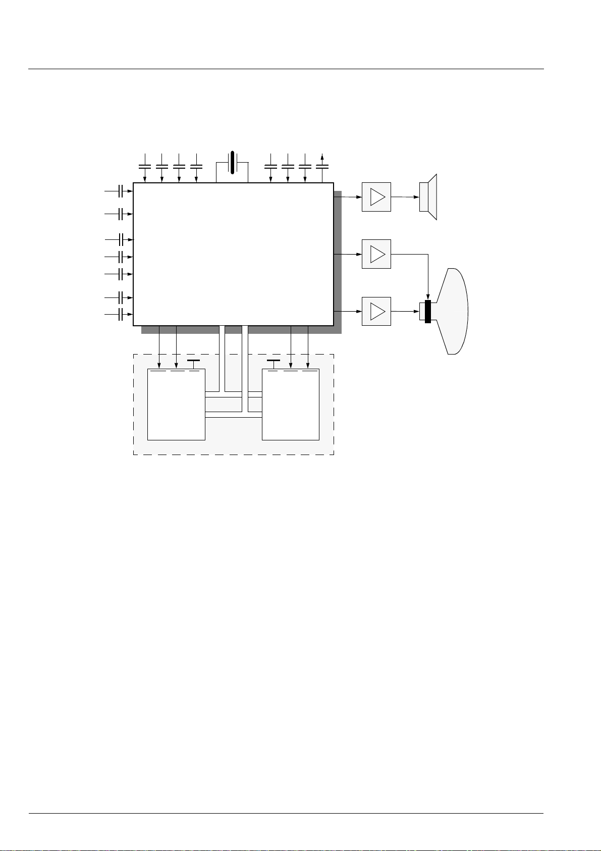
1.3. System Application
Analog Video
CVBS1
CVBS2
Analog RGB
R
Y
C
r
C
b
Y
C
GBFB
20.25 MHz
VCT 38xxA
512 kB
SRAM
DB
ADB
Analog Audio
Tuner/SCART/FrontAV
CECEOE2WE2
512 kB
ROM/
FLASH
OE1
WE1
Loudspeaker
CRT
optional memory extension
Fig. 1–3: Single-chip TV with VCT 38xxA
10 Micronas
Page 11
ADVANCE INFORMATION VCT 38xxA
2. Video Processing
2.1. Introduction
The VCT 38xxA includes complete video, display, and
deflection processing. In the following sections the
video processing part of the VCT 38xxA will be named
VDP for short.
All processing is done digitally, the video front-end and
video back-end are interfacing to the analog world.
Most functions of the VDP can be controlled by software via I
2
C bus slave interface (see Section 2.15. on
page 32).
2.2. Video Front-end
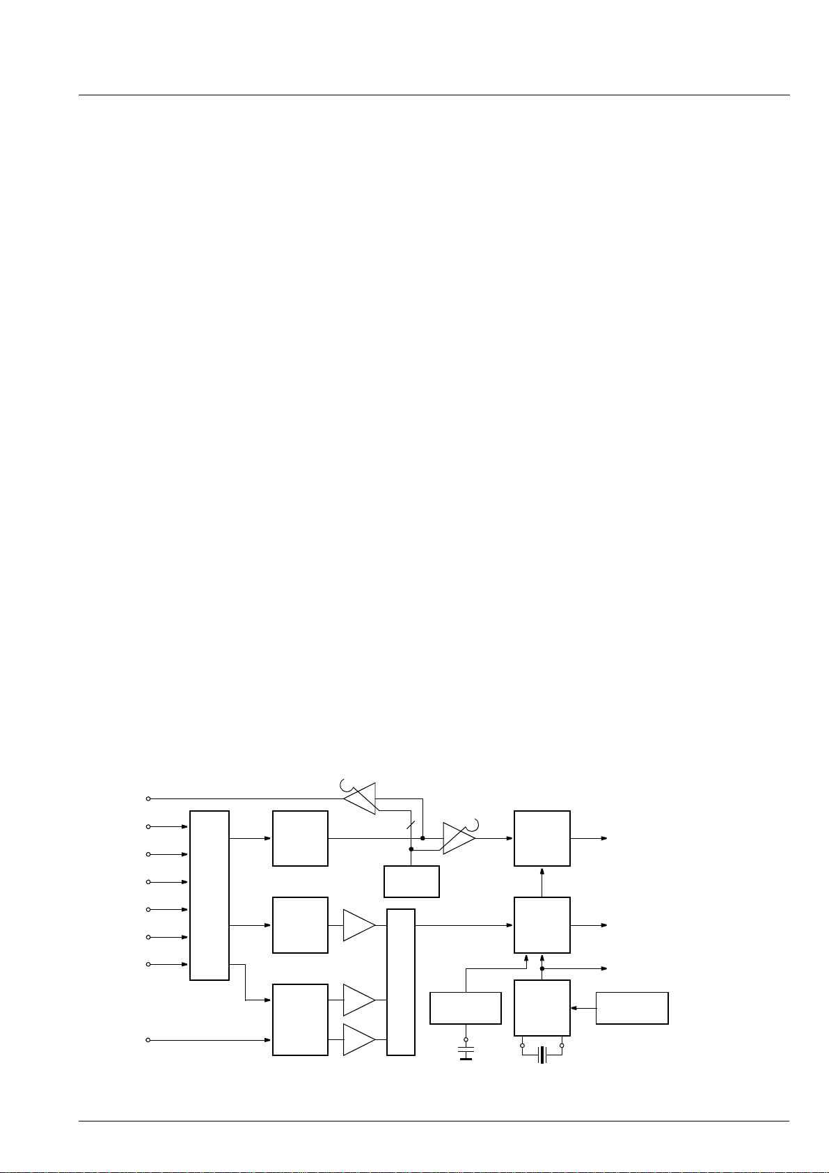
This block provides the analog interfaces to all video
inputs and mainly carries out analog-to-digital conversion for the following digital video processing. A block
diagram is given in Fig. 2–1.
Most of the functional blocks in the front-end are digitally controlled (clamping, AGC, and clock-DCO). The
control loops are closed by the Fast Processor (‘FP’)
embedded in the video decoder.
2.2.2. Clamping
The composite video input signals are AC-coupled to
the IC. The clamping voltage is stored on the coupling
capacitors and is generated by digitally controlled current sources. The clamping level is the back porch of
the video signal. S-VHS chrominance is also AC-coupled. The input pin is internally biased to the center of
the ADC input range. The chrominance inputs for
need to be AC-coupled by 220 nF clamping
YC
rCb
capacitors. It is strongly recommended to use 5-MHz
anti-alias low-pass filters on each input. Each channel
is sampled at 10.125 MHz with a resolution of 8 bit and
a clamping level of 128.
2.2.3. Automatic Gain Control
A digitally working automatic gain control adjusts the
magnitude of the selected baseband by +6/–4.5 dB in
64 logarithmic steps to the optimal range of the ADC.
The gain of the video input stage including the ADC is
213 steps/V with the AGC set to 0 dB. The gain of the
chrominance path in the YC
adapted to a nominal amplitude of 0.7 V
mode is fix and
rCb
. However, if
pp
an overflow of the ADC occurs an extended signal
range from 1 V
can be selected.
pp
2.2.1. Input Selector
Up to seven analog inputs can be connected. Four
inputs are for input of composite video or S-VHS luma
signal. These inputs are clamped to the sync back
porch and are amplified by a variable gain amplifier.
Two chroma inputs can be used for connection of
S-VHS carrier-chrominance signal. These inputs are
internally biased and have a fixed gain amplifier. For
analog YC
signals (e.g. from DVD players) one of
rCb
the selected luminance inputs is used together with
CBIN and CRIN inputs.
CVBS/Y
CVBS/Y
CVBS/Y
CVBS/Y
CVBS/Y
Chroma
Chroma
VOUT
VIN1
VIN2
VIN3
VIN4
CIN1
CIN2
CRIN
3
Clamp
Gain
Input
Mux
Bias ADC
Clamp
Chroma
CBIN
mux
2.2.4. Analog-to-Digital Converters
Two ADCs are provided to digitize the input signals.
Each converter runs with 20.25 MHz and has 8 bit resolution. An integrated bandgap circuit generates the
required reference voltages for the converters. The two
ADCs are of a 2-stage subranging type.
AGC
+6/–4.5 dB
ADC
digital CVBS or Luma
digital Chroma
System Clocks
Reference
Generation
DVCO
±150
ppm
Frequency
20.25 MHz
Fig. 2–1: Video front-end
Micronas 11
Page 12

VCT 38xxA ADVANCE INFORMATION
2.2.5. Digitally Controlled Clock Oscillator
The clock generation is also a part of the analog frontend. The crystal oscillator is controlled digitally by the
control processor. The clock frequency can be
adjusted within
±150 ppm.
2.2.6. Analog Video Output
The input signal of the Luma ADC is available at the
analog video output pin. The signal at this pin must be
buffered by a source follower. The output voltage is
2 V, thus the signal can be used to drive a 75-
Ω line.
The magnitude is adjusted with an AGC in 8 steps
together with the main AGC.
2.3. Adaptive Comb Filter
The adaptive comb filter is used for high-quality luminance/chrominance separation for PAL or NTSC signals. The comb filter improves the luminance resolution (bandwidth) and reduces interferences like
cross-luminance and cross-color artifacts. The adaptive algorithm can eliminate most of the mentioned
errors without introducing new artifacts or noise.
A block diagram of the comb filter is shown in Fig. 2–2.
The filter uses two line delays to process the information of three adjacent video lines. To have a fixed
phase relationship of the color subcarrier in the three
channels, the system clock (20.25 MHz) is fractionally
locked to the color subcarrier. This allows the processing of all color standards and substandards using a
single crystal frequency.
The CVBS signal in the three channels is filtered at the
subcarrier frequency by a set of bandpass/notch filters. The output of the three channels is used by the
adaption logic to select the weighting that is used to
reconstruct the luminance/chrominance signal from
the 4 bandpass/notch filter signals. By using soft mixing of the 4 signals switching artifacts of the adaption
algorithm are completely suppressed.
The comb filter uses the middle line as reference,
therefore, the comb filter delay is one line. If the comb
filter is switched off, the delay lines are used to pass
the luma/ chroma signals from the A/D converters to
the luma/ chroma outputs. Thus, the comb filter delay
is always one line.
Various parameters of the comb filter are adjustable,
hence giving to the user the ability to adjust his own
desired picture quality.
Two parameters (KY, KC) set the global gain of luma
and chroma comb separately; these values directly
weigh the adaption algorithm output. In this way, it is
possible to obtain a luma/chroma separation ranging
from standard notch/bandpass to full comb decoding.
The parameter KB allows to choose between the two
proposed comb booster modes. This so-called feature
widely improves vertical high-to-low frequency transitions areas, the typical example being a multiburst to
DC change. For KB=0, this improvement is kept moderate, whereas, in case of KB=1, it is maximum, but
the risk to increase the “hanging dots” amount for
some given color transitions is higher.
Using the default setting, the comb filter has separate
luma and chroma decision algorithms; however, it is
possible to switch the chroma comb factor to the current luma adaption output by setting CC to 1.
Another interesting feature is the programmable limitation of the luma comb amount; proper limitation, associated to adequate luma peaking, gives rise to an
enhanced 2-D resolution homogeneity. This limitation
is set by the parameter CLIM, ranging from 0 (no limitation) to 31 (max. limitation).
The DAA parameter (1:off, 0:on) is used to disable/
enable a very efficient built-in “rain effect” suppressor;
many comb filters show this side effect which gives
some vertical correlation to a 2-D uniform random
area, due to the vertical filtering. This unnatural-looking phenomenon is mostly visible on tuner images,
since they are always corrupted by some noise; and
this looks like rain.
Bandpass
Filter
CVBS Input
Chroma Input
1H Delay Line
1H Delay Line
Bandpass/
Notch
Filter
Bandpass
Filter
Luma / Chroma Mixers
Adaption Logic
Luma Output
Chroma Output
Fig. 2–2: Block diagram of the adaptive comb filter (PAL mode)
12 Micronas
Page 13
ADVANCE INFORMATION VCT 38xxA
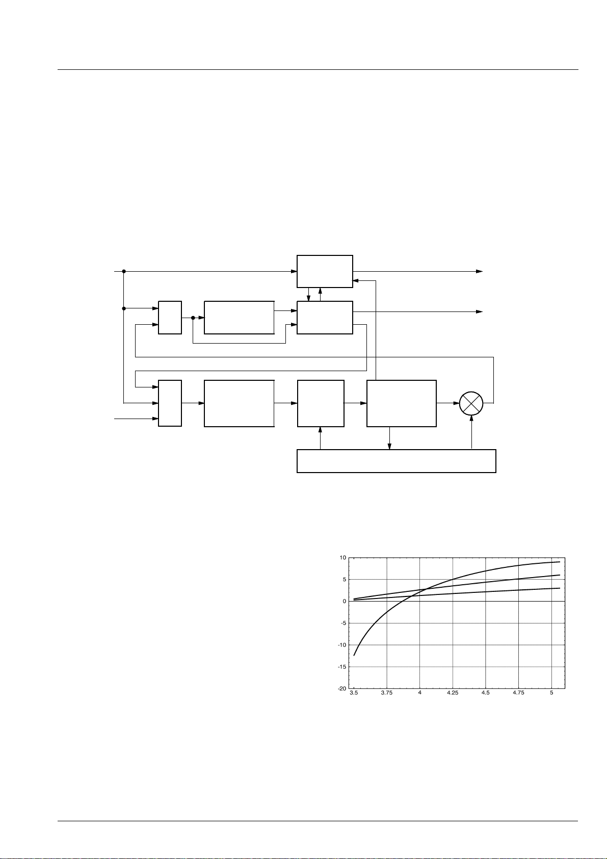
2.4. Color Decoder
In this block, the standard luma/chroma separation and
multi-standard color demodulation is carried out. The
color demodulation uses an asynchronous clock, thus
allowing a unified architecture for all color standards.
A block diagram of the color decoder is shown in Fig.
2–3. The luma as well as the chroma processing, is
shown here. The color decoder provides also some
special modes, e.g. wide band chroma format which is
intended for S-VHS wide bandwidth chroma.
Luma / CVBS
MUXMUX
1 H Delay
If the adaptive comb filter is used for luma chroma separation, the color decoder uses the S-VHS mode processing. The output of the color decoder is YC
4:2:2 format.
Notch
Filter
CrossSwitch
Luma
Chroma
rCb
in a
IF Compensation
Chroma
DC-Reject
Fig. 2–3: Color decoder
2.4.1. IF-Compensation
With off-air or mistuned reception, any attenuation at
higher frequencies or asymmetry around the color
subcarrier is compensated. Four different settings of
the IF-compensation are possible:
– flat (no compensation)
– 6 dB/octave
– 12 dB/octave
– 10 dB/MHz
Mixer
Low-pass Filter
ACC
Phase/Freq
Demodulator
ColorPLL/ColorACC
The last setting gives a very large boost to high frequencies. It is provided for SECAM signals that are
decoded using a SAW filter specified originally for the
PAL standard.
Fig. 2–4: Frequency response of chroma IF-compensation
Micronas 13
Page 14

VCT 38xxA ADVANCE INFORMATION
PAL/NTSC
SECAM
2.4.2. Demodulator
The entire signal (which might still contain luma) is
now quadrature-mixed to the baseband. The mixing
frequency is equal to the subcarrier for PAL and NTSC,
thus achieving the chroma demodulation. For SECAM,
the mixing frequency is 4.286 MHz giving the quadrature baseband components of the FM modulated
chroma. After the mixer, a low-pass filter selects the
chroma components; a downsampling stage converts
the color difference signals to a multiplexed half-rate
data stream.
The subcarrier frequency in the demodulator is generated by direct digital synthesis; therefore, substandards such as PAL 3.58 or NTSC 4.43 can also be
demodulated.
2.4.3. Chrominance Filter
The demodulation is followed by a low-pass filter for
the color difference signals for PAL/NTSC. SECAM
requires a modified low-pass function with bell-filter
characteristic. At the output of the low-pass filter, all
luma information is eliminated.
The low-pass filters are calculated in time multiplex for
the two color signals. Three bandwidth settings (narrow, normal, broad) are available for each standard.
For PAL/NTSC, a wide band chroma filter can be
selected. This filter is intended for high bandwidth
chroma signals, e.g. a non-standard wide bandwidth
S-VHS signal.
2.4.4. Frequency Demodulator
The frequency demodulator for demodulating the
SECAM signal is implemented as a CORDIC structure.
It calculates the phase and magnitude of the quadrature components by coordinate rotation.
The phase output of the CORDIC processor is differentiated to obtain the demodulated frequency. After
the deemphasis filter, the Dr and Db signals are scaled
to standard C
switch.
2.4.5. Burst Detection / Saturation Control
In the PAL/NTSC-system the burst is the reference for
the color signal. The phase and magnitude outputs of
the CORDIC are gated with the color key and used for
controlling the phase-locked-loop (APC) of the demodulator and the automatic color control (ACC) in PAL/
NTSC.
The ACC has a control range of +30...
Color saturation can be selected once for all color
standards. In PAL/NTSC it is used as reference for the
ACC. In SECAM the necessary gains are calculated
automatically.
For SECAM decoding, the frequency of the burst is
measured. Thus, the current chroma carrier frequency
can be identified and is used to control the SECAM
processing. The burst measurements also control the
color killer operation; they are used for automatic standard detection as well.
amplitudes and fed to the crossover
rCb
−6 dB.
Fig. 2–5: Frequency response of chroma filters
2.4.6. Color Killer Operation
The color killer uses the burst-phase/burst-frequency
measurement to identify a PAL/NTSC or SECAM color
signal. For PAL/NTSC, the color is switched off (killed)
as long as the color subcarrier PLL is not locked. For
SECAM, the killer is controlled by the toggle of the
burst frequency. The burst amplitude measurement is
used to switch-off the color if the burst amplitude is
below a programmable threshold. Thus, color will be
killed for very noisy signals. The color amplitude killer
has a programmable hysteresis.
14 Micronas
Page 15
ADVANCE INFORMATION VCT 38xxA
2.4.7. Automatic Standard Recognition
The burst-frequency measurement is also used for
automatic standard recognition (together with the status of horizontal and vertical locking) thus allowing a
completely independent search of the line and color
CVBS
8
Notch
filter
Chroma
Process.
Y
C C
a) conventional b) S-VHS
r b
Luma
8
chroma
8
Chroma
Process.
Y
C C
r b
standard of the input signal. The following standards
can be distinguished:
PAL B,G,H,I; NTSC M; SECAM; NTSC 44; PAL M;
CVBS
8
Notch
filter
Y
PAL N; PA L 6 0
1 H
Delay
C C
r b
For a preselection of allowed standards, the recognition can be enabled/disabled via I
2
C bus for each stan-
Chroma
Process.
c) compensated
dard separately.
If at least one standard is enabled, the VCT 38xxA regularly checks the horizontal and vertical locking of the
CVBS
Notch
1 H
8
Delay
filter
Y
input signal and the state of the color killer. If an error
exists for several adjacent fields a new standard
search is started. Depending on the measured line
number and burst frequency, the current standard is
selected.
For error handling the recognition algorithm delivers
the following status information:
Chroma
Process.
d) comb filter
Fig. 2–6: NTSC color decoding options
C C
r b
– search active (busy)
– search terminated, but failed
– found standard is disabled
– vertical standard invalid
– no color found
2.4.8. PAL Compensation/1-H Comb Filter
The color decoder uses one fully integrated delay line.
Only active video is stored.
The delay line application depends on the color standard:
– NTSC: 1-H comb filter or color compensation
– PAL: color compensation
– SECAM: crossover switch
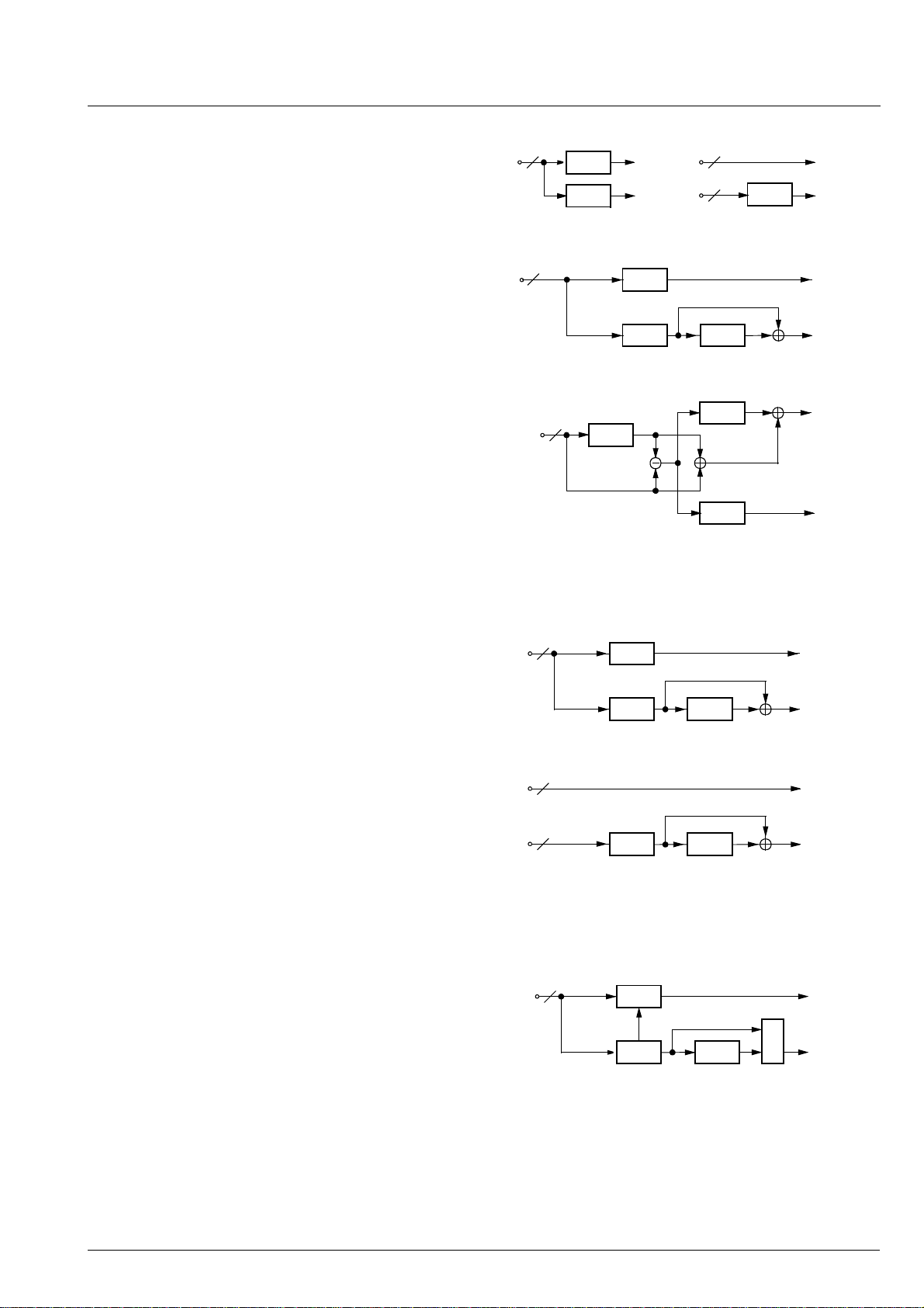
In the NTSC compensated mode, (Fig. 2–6c), the color
signal is averaged for two adjacent lines. Thus,
cross-color distortion and chroma noise is reduced. In
the NTSC comb filter mode, (Fig. 2–6d), the delay line
is in the composite signal path, thus allowing reduction
of cross-color components, as well as cross-luminance. The loss of vertical resolution in the luminance
channel is compensated by adding the vertical detail
signal with removed color information.
CVBS
8
Notch
filter
Chroma
Process.
1 H
Delay
a) conventional
Luma
8
Chroma
8
Chroma
Process.
1 H
Delay
b) S-VHS
Fig. 2–7: PAL color decoding options
CVBS
8
Notch
filter
Chroma
Process.
1 H
Delay
Fig. 2–8: SECAM color decoding
MUX
Y
C C
r b
Y
C C
r b
Y
C C
r b
Micronas 15
Page 16
VCT 38xxA ADVANCE INFORMATION
dB
MHz
10
02 4 6 8 10
0
–10
–20
–30
–40
dB
MHz
10
02 4 6 8 10
0
–10
–20
–30
–40
PAL/NTSC notch filter
SECAM notch filter
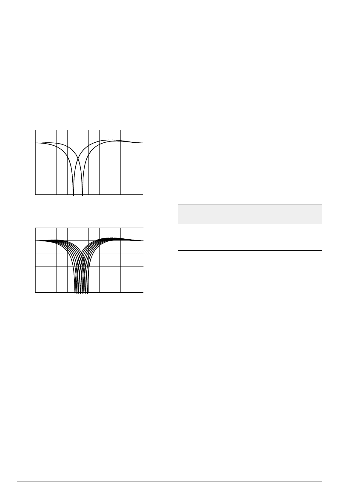
2.4.9. Luminance Notch Filter
If a composite video signal is applied, the color information is suppressed by a programmable notch filter.
The position of the filter center frequency depends on
the subcarrier frequency for PAL/NTSC. For SECAM,
the notch is directly controlled by the chroma carrier
frequency. This considerably reduces the cross-luminance. The frequency responses for all three systems
are shown in Fig. 2–9.
2.5. Horizontal Scaler
The 4:2:2 YC
signal from the color decoder is pro-
rCb
cessed by the horizontal scaler. The scaler block
allows a linear or nonlinear horizontal scaling of the
input video signal in the range of 0.25 to 4. Nonlinear
scaling, also called “Panoramavision”, provides a geometrical distortion of the input picture. It is used to fit a
picture with 4:3 format on a 16:9 screen by stretching
the picture geometry at the borders. Also, the inverse
effect can be produced by the scaler. A summary of
scaler modes is given in Table 2–1.
The scaler contains a programmable decimation filter,
a 1-line FIFO memory, and a programmable interpolation filter. The scaler input filter is also used for pixel
skew correction (see Section 2.4.10. on page 16). The
decimator/interpolator structure allows optimal use of
the FIFO memory. The controlling of the scaler is done
by the internal Fast Processor.
Table 2–1: Scaler modes
Mode Scale
Description
Factor
Fig. 2–9: Frequency responses of the luma
notch filter for PAL, NTSC, SECAM
2.4.10.Skew Filtering
The system clock is free-running and not locked to the
TV line frequency. Therefore, the ADC sampling pattern is not orthogonal. The decoded YC
converted to an orthogonal sampling raster by the
signals are
rCb
skew filters, which are part of the scaler block.
The skew filters allow the application of a group delay
to the input signals without introducing waveform or
frequency response distortion.
The amount of phase shift of this filter is controlled by
the horizontal PLL1. The accuracy of the filters is 1/32
clocks for luminance and 1/4 clocks for chroma. Thus
the 4:2:2 YC
data is in an orthogonal pixel format
rCb
even in the case of nonstandard input signals such as
VCR.
Compression
4:3
→ 16:9
0.75
linear
4:3 source displayed on
a 16:9 tube,
with side panels
Panorama
4:3
→16:9
Zoom
4:3
→ 4:3
nonlinear
compr
1.33
linear
4:3 source displayed on
a 16:9 tube,
Borders distorted
Letterbox source (PAL+)
displayed on a 4:3 tube,
vertical overscan with
cropping of side panels
Panorama
→ 4:3
4:3
nonlinear
zoom
Letterbox source (PAL+)
displayed on a 4:3 tube,
vertical overscan, borders distorted, no cropping
2.6. Black-line Detector
In case of a letterbox format input video, e.g. Cinemascope, PAL+ etc., black areas at the upper and lower
part of the picture are visible. It is suitable to remove or
reduce these areas by a vertical zoom and/or shift
operation.
The VCT 38xxA supports this feature by a letterbox
detector. The circuitry detects black video lines by
measuring the signal amplitude during active video.
For every field the number of black lines at the upper
and lower part of the picture are measured, compared
to the previous measurement and the minima are
stored in the I
2
C-register BLKLIN. To adjust the picture
16 Micronas
Page 17
ADVANCE INFORMATION VCT 38xxA
amplitude, the external controller reads this register,
calculates the vertical scaling coefficient and transfers
the new settings, e.g. vertical sawtooth parameters,
horizontal scaling coefficient etc., to the VCT 38xxA.
Letterbox signals containing logos on the left or right
side of the black areas are processed as black lines,
while subtitles, inserted in the black areas, are processed as non-black lines. Therefore, the subtitles are
visible on the screen. To suppress the subtitles, the
vertical zoom coefficient is calculated by selecting the
larger number of black lines only. Dark video scenes
with a low contrast level compared to the letterbox area
are indicated by the BLKPIC bit.
2.7. Test Pattern Generator
The YC
where YC
outputs can be switched to a test mode
rCb
data are generated digitally in the
rCb
VCT 38xxA. Test patterns include luma/chroma ramps
and flat fields.
2.8. Video Sync Processing
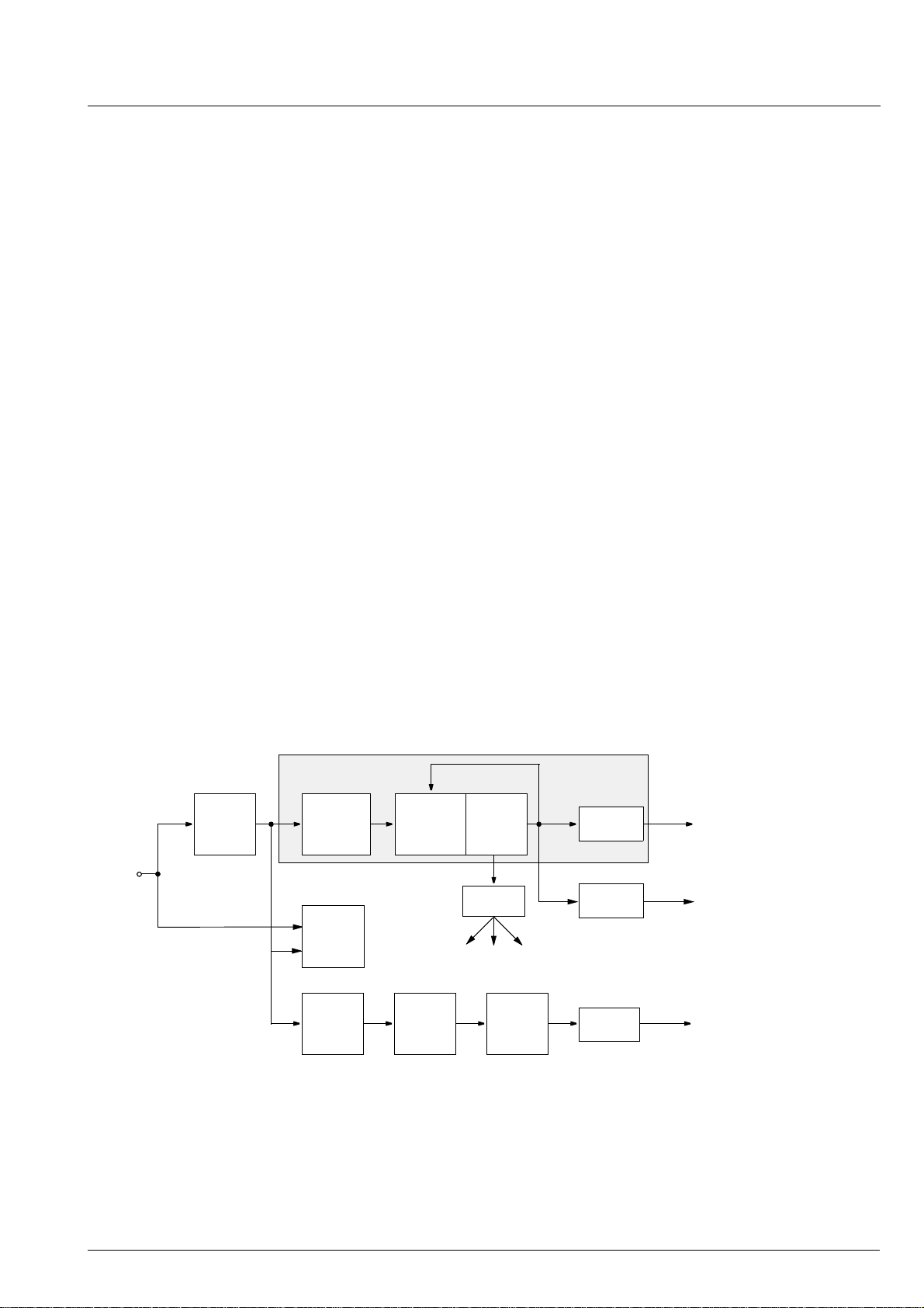
Fig. 2–10 shows a block diagram of the front-end sync
processing. To extract the sync information from the
video signal, a linear phase low-pass filter eliminates
all noise and video contents above 1 MHz. The sync is
separated by a slicer; the sync phase is measured. A
variable window can be selected to improve the noise
immunity of the slicer. The phase comparator mea-
sures the falling edge of sync, as well as the integrated
sync pulse.
The sync phase error is filtered by a phase-locked loop
that is computed by the FP. All timing in the front-end is
derived from a counter that is part of this PLL, and it
thus counts synchronously to the video signal.
A separate hardware block measures the signal back
porch and also allows gathering the maximum/minimum of the video signal. This information is processed
by the FP and used for gain control and clamping.
For vertical sync separation, the sliced video signal is
integrated. The FP uses the integrator value to derive
vertical sync and field information.
The information extracted by the video sync processing is multiplexed onto the hardware front sync signal
(FSY) and is distributed to the rest of the video processing system.
The data for the vertical deflection, the sawtooth, and
the East-West correction signal is calculated by the
VCT 38xxA. The data is buffered in a FIFO and transferred to the back-end by a single wire interface.
Frequency and phase characteristics of the analog
video signal are derived from PLL1. The results are fed
to the scaler unit for data interpolation and orthogonalization and to the clock synthesizer for line-locked
clock generation. Horizontal and vertical syncs are
latched with the line-locked clock.
video
input
low-pass
1 MHz
&
sync slicer
Horizontal
Sync
Separation
Clamp &
Signal
Meas.
Vertical
Sync
Separation
Fig. 2–10: Sync separation block diagram
Phase
Separator
Low-pass
clamping, colorkey, FIFO_write
Sawtooth
Parabola
Calculation
counter
&
Front-end
Timing
FIFO
PLL1
Generator
Synthesizer
Front
Sync
Clock
Syncs
Vertical
Serial
Data
Front Sync
Skew
Vblank
Field
Clock
H/V Syncs
Vertical
E/W
Sawtooth
Micronas 17
Page 18
VCT 38xxA ADVANCE INFORMATION
2.9. Macrovision Detection
Video signals from Macrovision encoded VCR tapes
are decoded without loss of picture quality. However, it
might be necessary in some applications to detect the
presence of Macrovision encoded video signals. This
is possible by reading the Macrovision status register
(FP-RAM 0x170).
Macrovision encoded video signals typically have AGC
pulses and pseudo sync pulses added during VBI. The
amplitude of the AGC pulses is modulated in time. The
Macrovision detection logic measures the VBI lines
and compares the signal against thresholds.
The window wherein the video lines are checked for
Macrovision pulses can be defined in terms of start
and stop line (e.g. 6-15 for NTSC).
2.10.Display Processing
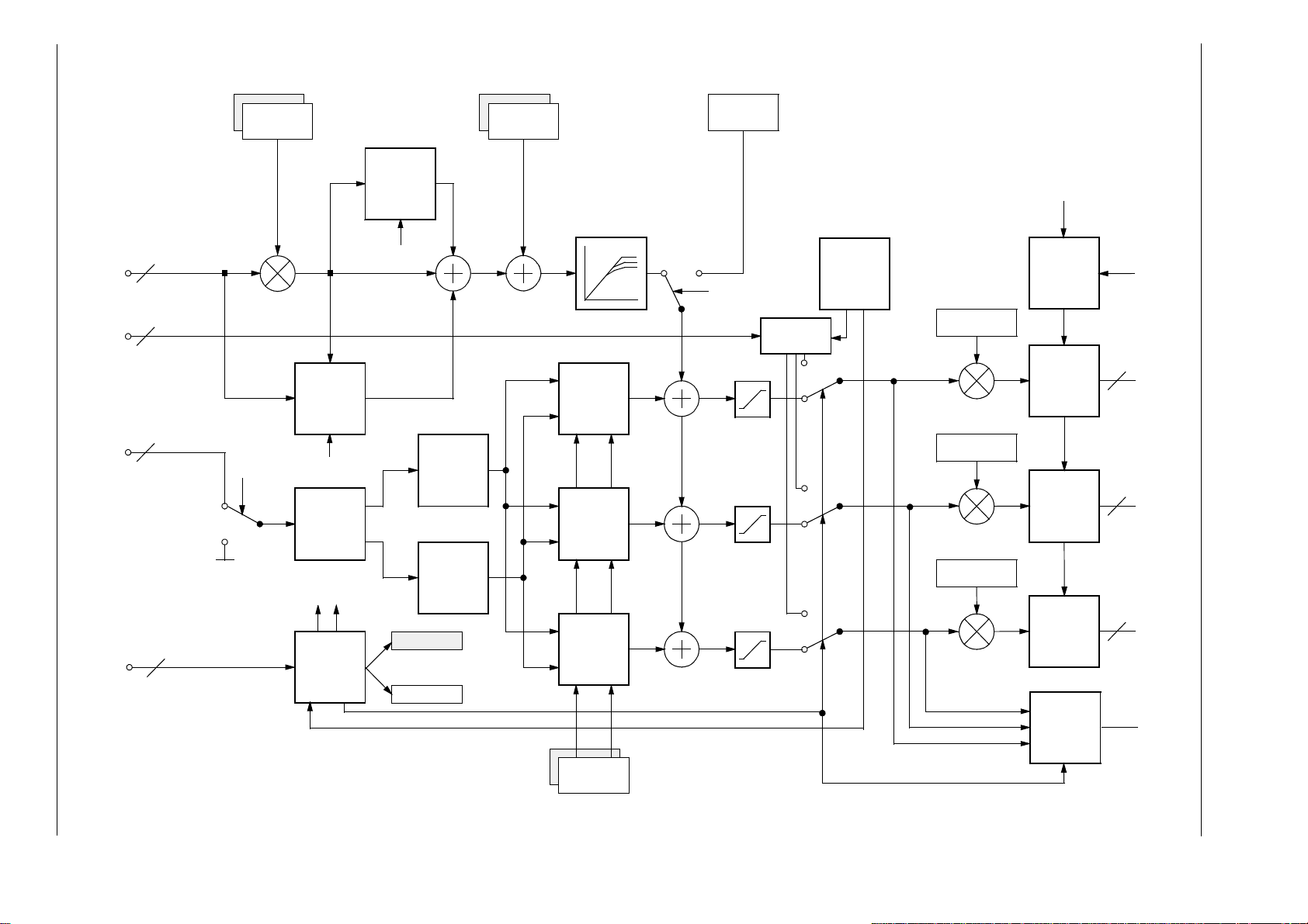
In the display processing the conversion from digital
to analog RGB is carried out. A block diagram is
YC
rCb
shown in Fig. 2–18 on page 24. In the luminance processing path, contrast and brightness adjustments and
a variety of features, such as black-level expansion,
dynamic peaking and soft limiting, are provided. In the
chrominance path, the C
signals are converted to
rCb
4:4:4 format and filtered by a color transient improvement circuit. The YC
signals are converted by a
rCb
programmable matrix to RGB color space.
The display processor provides separate control settings for two pictures, i.e. different coefficients for a
‘main’ and a ‘side’ picture.
The digital OSD insertion circuit allows the insertion of
a 5-bit OSD signal. The color space for this signal is
controlled by a partially programmable color look-up
table (CLUT) and contrast adjustment.
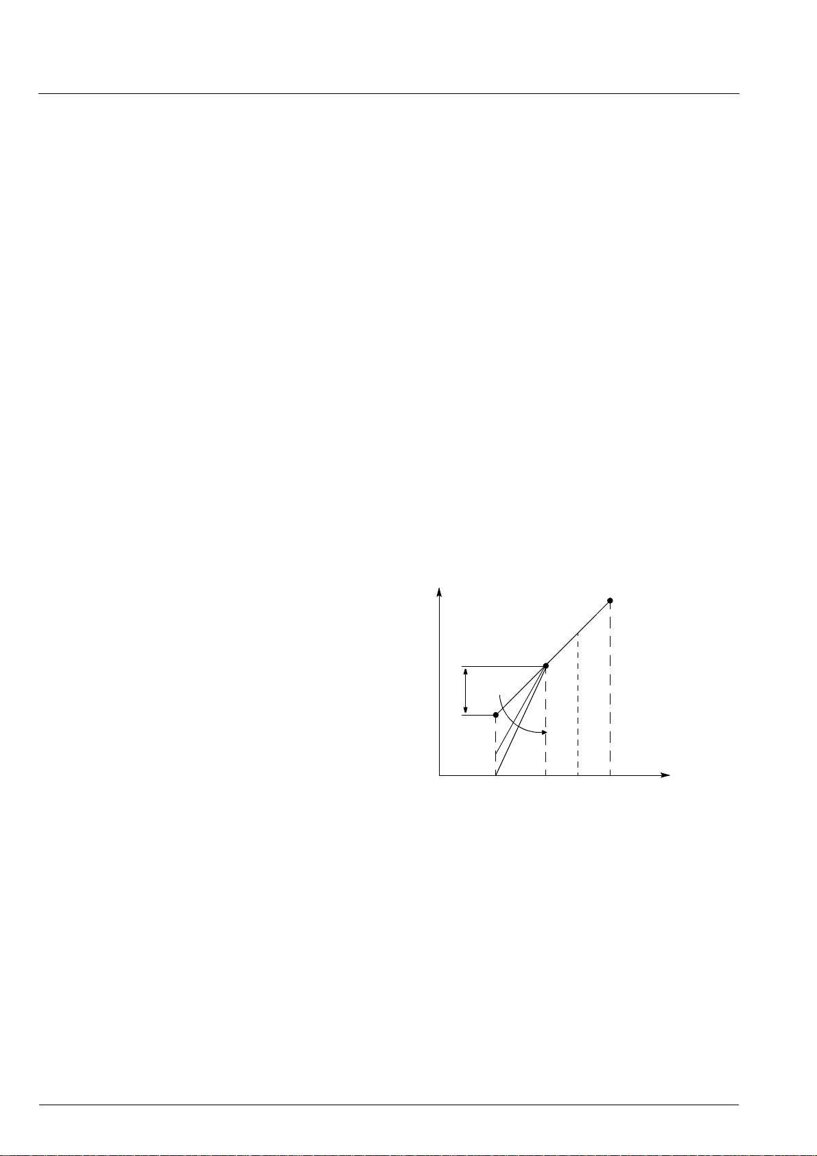
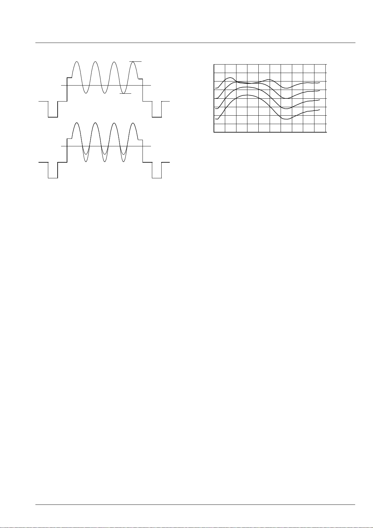
2.10.2.Black-Level Expander
The black-level expander enhances the contrast of the
picture. Therefore the luminance signal is modified
with an adjustable, non-linear function. Dark areas of
the picture are changed to black, while bright areas
remain unchanged. The advantage of this black-level
expander is that the black expansion is performed only
if it will be most noticeable to the viewer.
The black-level expander works adaptively. Depending
on the measured amplitudes ‘L
’ and ‘L
min
max
’ of the
low-pass-filtered luminance and an adjustable coefficient BTLT, a tilt point ‘L
= L
L
t
+ BTLT (L
min
’ is established by
t
- L
max
min
).
Above this value there is no expansion, while all luminance values below this point are expanded according
to:
= Lin + BAM (Lin - Lt)
L
out
A second threshold, L
, can be programmed, above
tr
which there is no expansion. The characteristics of the
black-level expander are shown in Fig. 2–11and Fig.
2–12.
L
out
L
BAM
BTLT
L
min
L
max
L
tr
t
The OSD signals and the display clock are synchronized to the horizontal flyback. For the display clock, a
L
BTHR
tr
L
in
gate delay phase shifter is used. In the analog backend, three 10-bit digital-to-analog converters provide
the analog output signals.
2.10.1.Luma Contrast Adjustment
Fig. 2–11: Characteristics of the black-level expander
The tilt point L
is a function of the dynamic range of
t
the video signal. Thus, the black-level expansion is
The contrast of the luminance signal can be adjusted
by multiplication with a 6-bit contrast value. The contrast value corresponds to a gain factor from 0 to 2,
where the value 32 is equivalent to a gain of 1. The
only performed when the video signal has a large
dynamic range. Otherwise, the expansion to black is
zero. This allows the correction of the characteristics of
the picture tube.
contrast can be adjusted separately for main picture
and side picture.
18 Micronas
Page 19
ADVANCE INFORMATION VCT 38xxA
a)
b)
L
max
L
t
L
min
L
t
Fig. 2–12: Black-level expansion
a) luminance input
b) luminance input and output
2.10.3.Dynamic Peaking
Especially with decoded composite signals and notch
filter luminance separation, as input signals, it is necessary to improve the luminance frequency characteristics. With transparent, high-bandwidth signals, it is
sometimes desirable to soften the image.
dB
20
15
10
5
0
–5
–10
–15
–20
02 4 6 8 10
MHz
Fig. 2–13: Dynamic peaking frequency response
In the VCT 38xxA, the luma response is improved by
‘dynamic’ peaking. The algorithm has been optimized
regarding step and frequency response. It adapts to
the amplitude of the high-frequency part. Small AC
amplitudes are processed, while large AC amplitudes
stay nearly unmodified.
The dynamic range can be adjusted from
−14 to
+14 dB for small high-frequency signals. There is separate adjustment for signal overshoot and for signal
undershoot. For large signals, the dynamic range is
limited by a non-linear function that does not create
any visible alias components. The peaking can be
switched over to “softening” by inverting the peaking
term by software.
The center frequency of the peaking filter is switchable
from 2.5 MHz to 3.2 MHz. For S-VHS and for notch filter
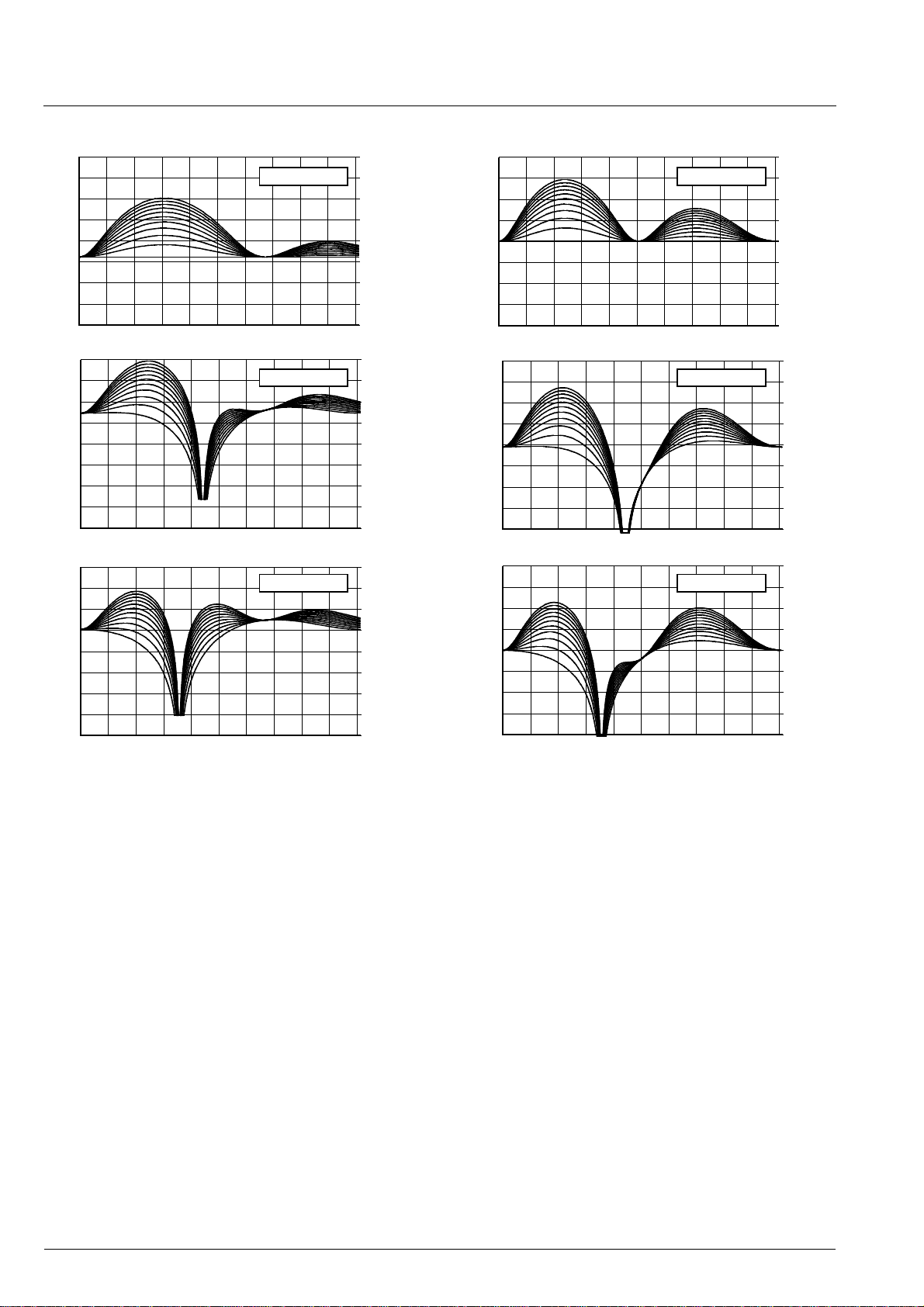
color decoding, the total system frequency responses
for both PAL and NTSC are shown in Fig. 2–14.
Transients, produced by the dynamic peaking when
switching video source signals, can be suppressed via
the priority bus.
Micronas 19
Page 20
VCT 38xxA ADVANCE INFORMATION
dB
20
15
10
5
0
-5
-10
-15
-20
02 4 6 8 10
dB
20
15
10
5
0
-5
-10
-15
-20
02 4 6 8 10
dB
20
15
10
5
0
-5
-10
-15
-20
02 4 6 8 10
CF=3.2 MHz
CF=3.2 MHz
CF=3.2 MHz
S-VHS
MHz
PAL/SECAM
MHz
NTSC
MHz
dB
20
15
10
5
0
-5
-10
-15
-20
02 4 6 8 10
dB
20
15
10
5
0
-5
-10
-15
-20
02 4 68 10
dB
20
15
10
5
0
-5
-10
-15
-20
02 4 68 10
CF=2.5 MHz
CF=2.5 MHz
CF=2.5 MHz
MHz
MHz
MHz
Fig. 2–14: Total frequency response for peaking filter and S-VHS, PAL, NTSC
20 Micronas
Page 21
ADVANCE INFORMATION VCT 38xxA
2.10.4.Digital Brightness Adjustment
The DC-level of the luminance signal can be adjusted
by adding an 8-bit number in the luminance signal path
in front of the softlimiter.
With a contrast adjustment of 32 (gain+1) the signal
can be shifted by 100 %. After the brightness addition,
the negative going signals are limited to zero. It is
desirable to keep a small positive offset with the signal
to prevent undershoots produced by the peaking from
being cut. The digital brightness adjustment works
separately for main and side picture.
2.10.5.Soft Limiter
The dynamic range of the processed luma signal must
be limited to prevent the CRT from overload. An appropriate headroom for contrast, peaking and brightness
can be adjusted by the TV manufacturer according to
the CRT characteristics. All signals above this limit will
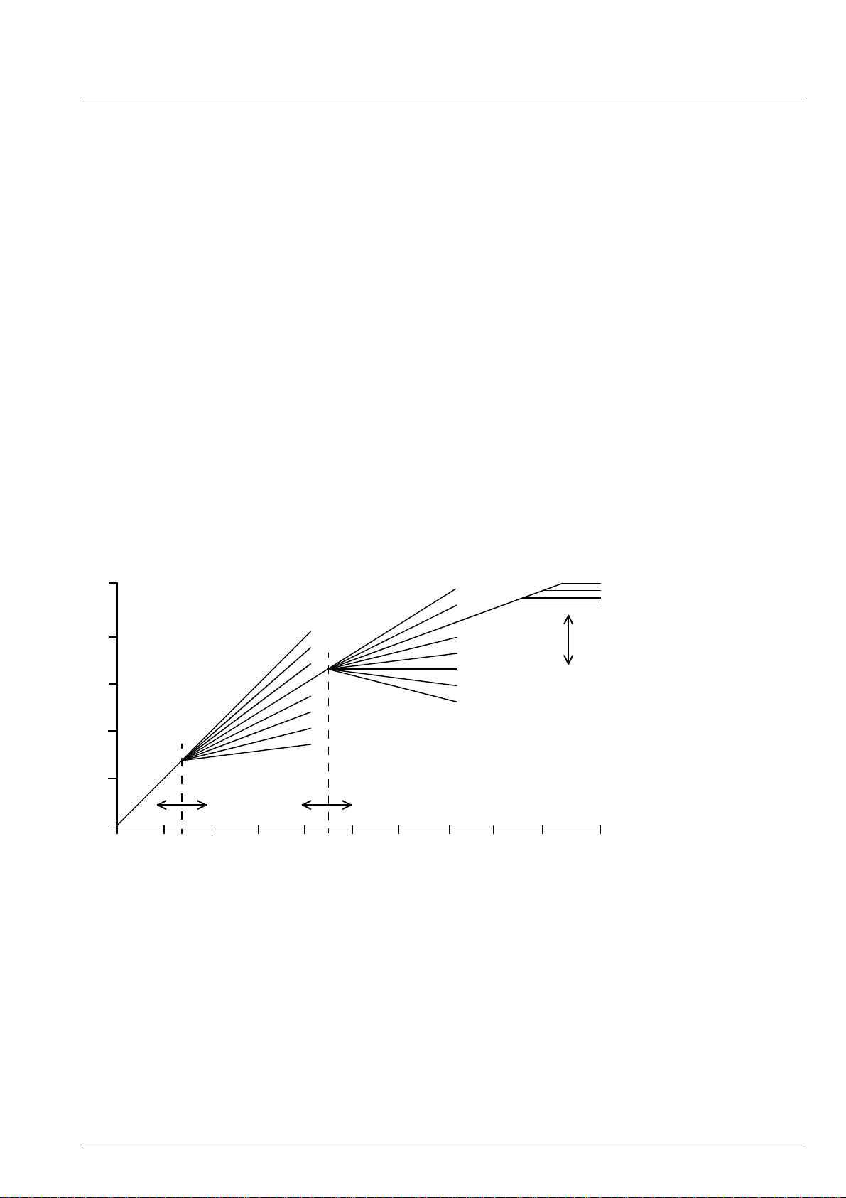
be ‘soft’-clipped. A characteristic diagram of the soft
limiter is shown in Fig. 2–15. The total limiter consists
of three parts:
Part 1 includes adjustable tilt point and gain. The gain
before the tilt value is 1. Above the tilt value, a part
(0...15/16) of the input signal is subtracted from the
input signal itself. Therefore, the gain is adjustable
from 16/16 to 1/16, when the slope value varies from
0 to 15. The tilt value can be adjusted from 0 to 511.
Part 2 has the same characteristics as part 1. The subtracting part is also relative to the input signal, so the
total differential gain will become negative if the sum of
slope 1 and slope 2 is greater than 16 and the input
signal is above the both tilt values (see characteristics).
Finally, the output signal of the soft limiter will be
clipped by a hard limiter adjustable from 256 to 511.
2.10.6.Chroma Interpolation
A linear phase interpolator is used to convert the
chroma sampling rate from 10.125 MHz (4:2:2) to
20.25 MHz (4:4:4). All further processing is carried out
at the full sampling rate.
Output
511
400
300
200
100
tilt 1 [ 0...511] tilt 2 [ 0...511]
0
0 100 200 300 400 500 600 700 800 900 1023
Part 1 Part 2
slope 1
[0...15]
0
2
4
6
8
10
12
14
0
2
4
6
8
10
12
14
slope 2
[0...15]
Hard limiter
range=
256...511
Fig. 2–15: Characteristic of soft limiter A and B and hard limiter
2.10.7.Chroma Transient Improvement
sharpened chroma signals are limited to a proper
value automatically.
The intention of this block is to enhance the chroma
resolution. A correction signal is calculated by differentiation of the color difference signals. The differentiation can be selected according to the signal bandwidth,
e.g. for PAL/NTSC/SECAM or digital component signals, respectively. The amplitude of the correction signal is adjustable. Small noise amplitudes in the correction signal are suppressed by an adjustable coring
circuit. To eliminate ‘wrong colors’, which are caused
by over and undershoots at the chroma transition, the
Calculation Example for the
Softlimiter Input Amplitude.
(The real signal processing in
the limiter is 2 bit more than
described here)
Y Input 16...235 (ITUR)
Black Level 16 (constant)
Contrast 63
Dig. Brightness 20
BLE off
Peaking off
Limiter input signal:
(Yin-Black Level)
(235-16)
Limiter Input
⋅Contr./32 + Brightn.
⋅ 63/32 + 20 = 451
Micronas 21
Page 22

VCT 38xxA ADVANCE INFORMATION
a) CrCb input of DTI
b) C
rCb
input + correction signal
c) sharpened and limited C
rCb
t
t
t
Cr in
C
b
in
a)
b)
Ampl.
C
r
out
C
b
out
c)
2.10.9.RGB Processing
After adding the post-processed luma, the digital RGB
signals are limited to 10 bits. Three multipliers are
used to digitally adjust the white drive. Using the same
multipliers an average beam current limiter is implemented (see Section 2.11.1. on page 25).
2.10.10.OSD Color Look-up Table
The VCT 38xxA has five input lines for an OSD signal.
This signal forms a 5-bit address for a color look-up
table (CLUT). The CLUT is a memory with 32 words
where each word holds a RGB value.
Bits 0 to 3 (bit 4=0) form the addresses for the ROM
part of the OSD, which generates full RGB signals (bit
0 to 2) and half-contrast RGB signals (bit 3).
Bit 4 addresses the RAM part of the OSD with 16
freely programmable colors, addressable with bit 0 to
3. The programming is done via the I
2
C bus.
Fig. 2–16: Digital color transient improvement
2.10.8.Inverse Matrix
A 6-multiplier matrix transcodes the C
and Cb signals
r
to R-Y, B-Y, and G-Y. The multipliers are also used to
adjust color saturation in the range of 0 to 2. The coefficients are signed and have a resolution of 9 bits.
There are separate matrix coefficients for main and
side pictures. The matrix computes:
−Y= MR1*C
R
G−Y= MG1*Cb+MR2*C
B−Y= MB1*Cb+MR2*C
+MR2*C
b
r
r
r
The initialization values for the matrix are computed
from the standard ITUR (CCIR) matrix:
R
G
B
1
0
1
1
−0.345
1.773
=
1.402
−0.713
0
Y
C
b
C
r
For a contrast setting of CTM+32, the matrix values
are scaled by a factor of 64 (see Table 2–4 on
page 34).
The amplitude of the CLUT output signals can be
adjusted separately for R, G, and B via the I
2
C bus.
The switchover between video RGB and OSD RGB is
done via the priority decoder.
2.10.11.Picture Frame Generator
When the picture does not fill the total screen (height
or width too small) it is surrounded with black areas.
These areas (and more) can be colored with the picture frame generator. This is done by switching over
the RGB signal from the matrix to the signal from the
OSD color look-up table.
The width of each area (left, right, upper, lower) can be
adjusted separately. The generator starts on the right,
respectively lower side of the screen and stops on the
left, respectively upper side of the screen. This means,
it runs during horizontal, respectively vertical flyback.
The color of the complete border can be stored in the
programmable OSD color look-up table in a separate
address. The format is 3 x 4-bit RGB. The contrast can
be adjusted separately.
The picture frame generator includes a priority master
circuit. Its priority is programmable and the border is
generated only if the priority is higher than the priority
of the other sources (video/OSD). Therefore, the border can be underlay or overlay depending on the picture source.
22 Micronas
Page 23
ADVANCE INFORMATION VCT 38xxA
2.10.12.Priority Decoder
The priority decoder selects the picture source
depending on the programmed priorities. Up to eight
levels can be selected for OSD and the picture frame –
where 0 is the highest. The video source always has
the lowest priority. A 5-bit information is attached to
each priority (see Table 2–4 on page 34). These bits
are programmable via the I
2
C bus and have the follow-
ing meanings:
– one of two contrast, brightness and matrix values for
main and side picture
– RGB from video signal or color look-up table
– disable/enable black-level expander
– disable/enable peaking transient suppression when
signal is switched
– disable/enable analog Fast-Blank input
RGB
N1 N2
Coring Gain1 Gain2
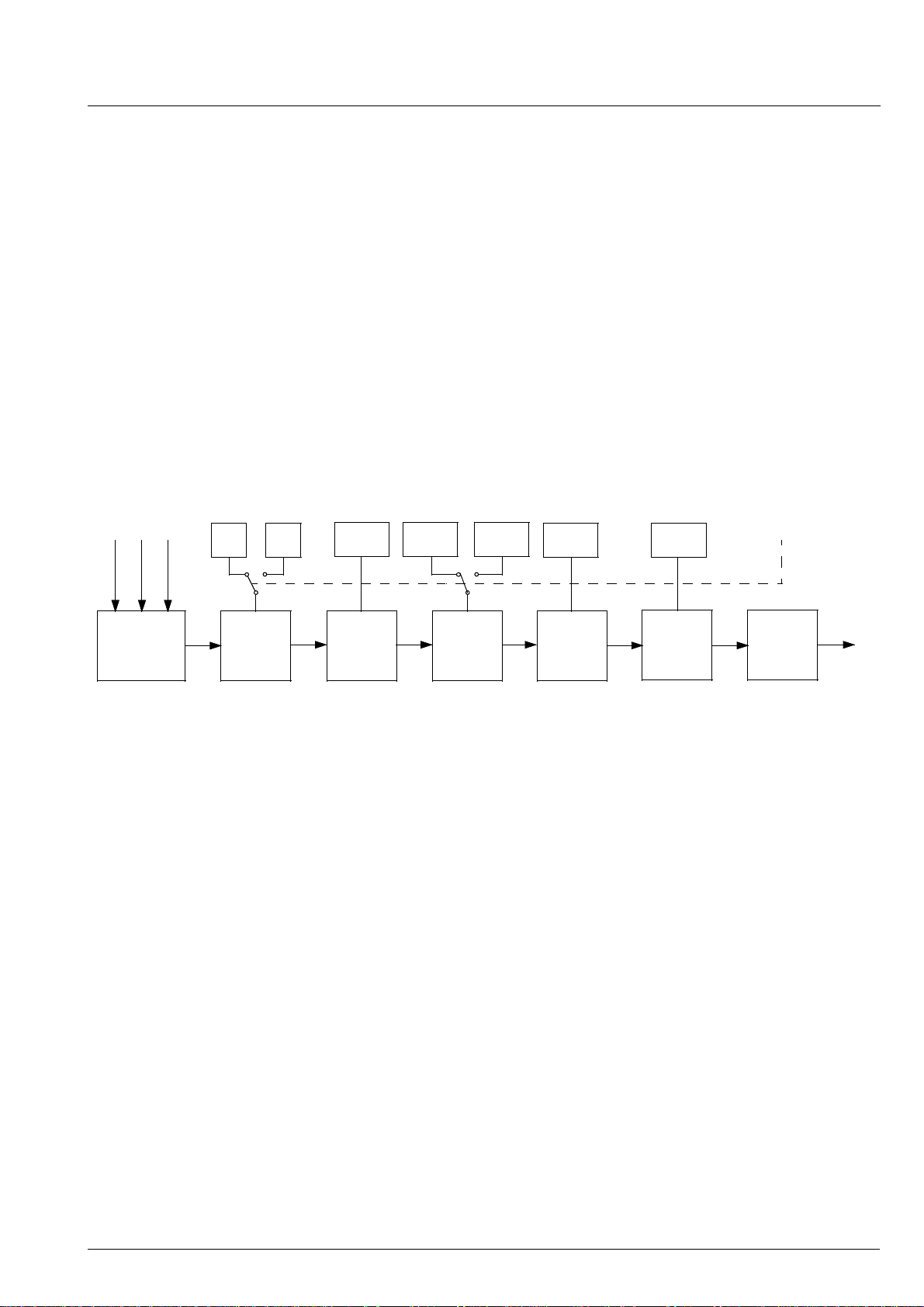
2.10.13.Scan Velocity Modulation
The RGB input signal of the SVM is converted to Y in a
simple matrix. Then the Y signal is differentiated by a
filter of the transfer function 1-Z
-N
, where N is programmable from 1 to 6. With a coring, some noise can be
suppressed. This is followed by a gain adjustment and
an adjustable limiter. The analog output signal is generated by an 8-bit D/A converter.
The signal delay can be adjusted by
±3.5 clocks in
half-clock steps. For the gain and filter adjustment
there are two parameter sets. The switching between
these two sets is done with the same RGB switch signal that is used for switching between video-RGB and
OSD-RGB for the RGB outputs (see Fig. 2–17).
RGB Switch
Limit Delay
Matrix and
Shaping
Modulation
Notch
Differentiator
-Nx
1-Z
Coring
adjustment
Gain
adjustment
Fig. 2–17: SVM Block diagram
2.10.14.Display Phase Shifter
A phase shifter is used to partially compensate the
phase differences between the video source and the
flyback signal. By using the described clock system,
this phase shifter works with an accuracy of approximately 1 ns. It has a range of 1 clock period which is
equivalent to
±24.7 ns at 20.25 MHz. The large
amount of phase shift (full clock periods) is realized in
the front-end circuit.
Limiter
Delay
adjustment
D/A
Converter
Output
Micronas 23
Page 24
24 Micronas
Fig. 2–18: Digital back-end
VCT 38xxA ADVANCE INFORMATION
dig.
Y in
8
5
dig. OSD in
8
dig.
in
C
rCb
Contrast
Expander
Blanking
for CRT Measurement
Black-
Level
prio
Interpol
4:4:4
Dynamic
peaking
prio
Cr
DTI
(C
Brightness
+ Offset
Softlimiter
White-Drive
Measurement
luma insert
for CRTmeasurement
Y
CLUT,
Contrast
Picture
Frame
Generator
White-Drive R
x beam Curr. Lim.
C
LOCK
Display
& Clock
Control
Phase
Horizontal
Flyback
dig.
Rout
Shift
Matrix
R’
)
r
R
White-Drive G
x Beam curr. Lim.
0...1 Clock
Phase
Matrix
G’
G
Shift
0...1 Clock
10
10
dig.
Gout
PRIO in
3
PRIO
Decoder
DTI
(C
Cb
Side Picture
select
Coefficients
Main Picture
White-Drive
)
b
x Beam Curr. Lim.
Phase
dig.
Bout
Shift
Matrix
B’
Matrix
Saturation
B
0...1 Clock
Scan
Velocity
Modulation
10
SVMout
Page 25
ADVANCE INFORMATION VCT 38xxA
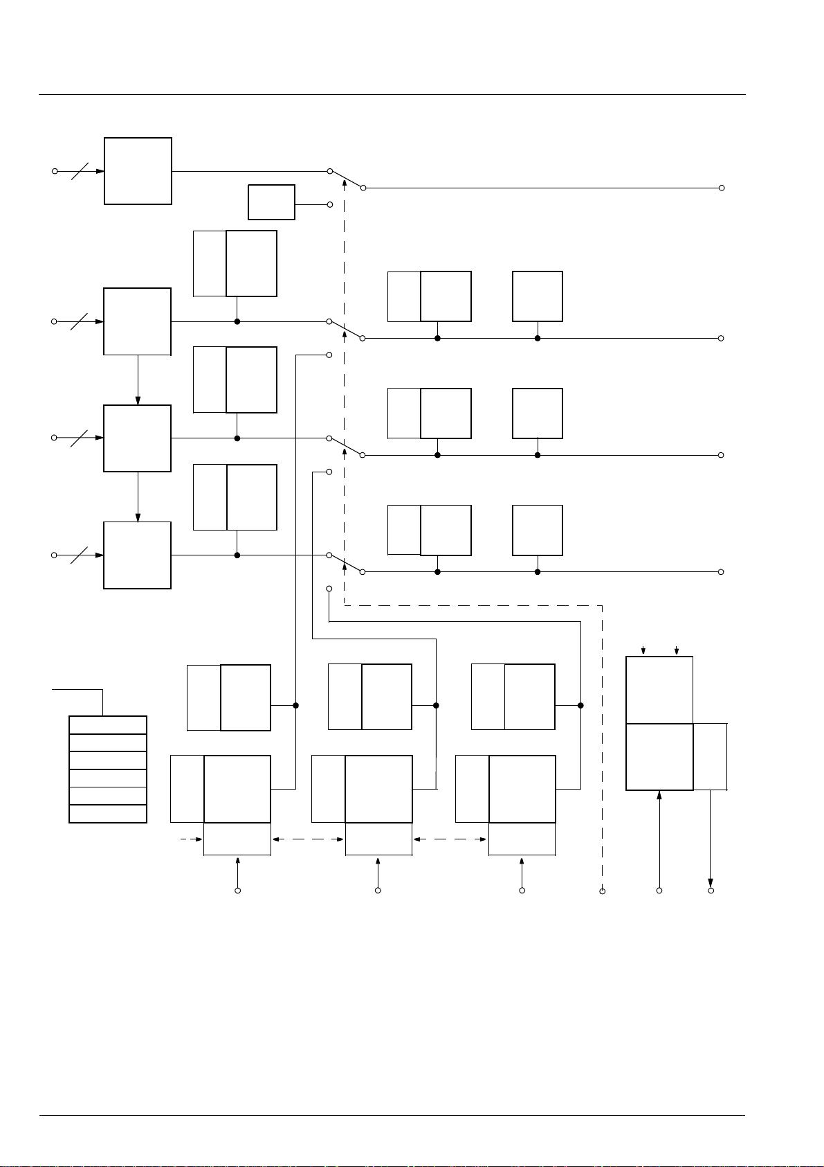
2.11.Video Back-end
The digital RGB signals are converted to analog RGBs
using three video digital-to-analog converters (DAC)
with 10-bit resolution. An analog brightness value is
provided by three additional DACs. The adjustment
range is 40 % of the full RGB range.
Controlling the white-drive/analog brightness and also
the external contrast and brightness adjustments is
done via the Fast Processor, located in the front-end.
Control of the cutoff DACs is done via I
2
C bus regis-
ters.
Finally cutoff and blanking values are added to the
RGB signals. Cutoff (dark current) is provided by three
9-bit DACs. The adjustment range is 60 % of full scale
RGB range.
The analog RGB-outputs are current outputs with current-sink characteristics. The maximum current drawn
by the output stage is obtained with peak white RGB.
An external half contrast signal can be used to reduce
the output current of the RGB outputs to 50 %.
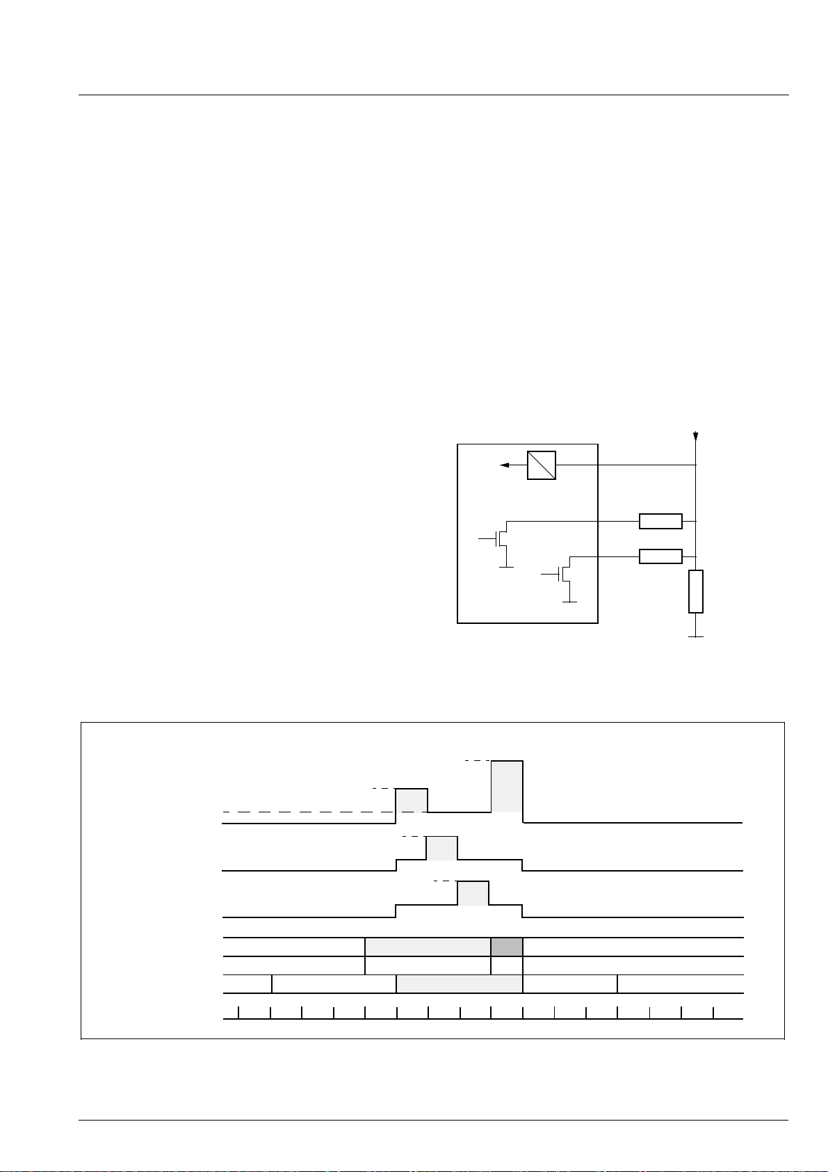
2.11.1.CRT Measurement and Control
The display processor is equipped with an 8-bit
PDM-ADC for all measuring purposes. The ADC is
connected to the SENSE input pin, the input range is 0
to 1.5V. The bandwidth of the PDM filter can be
selected; it is 40/80 kHz for small/large bandwidth setting. The input impedance is more than 1 M
Ω.
Cutoff and white-drive current measurement are carried out during the vertical blanking interval. They
always use the small bandwidth setting. The current
range for the cutoff measurement is set by connecting
a sense resistor to the MADC input. For the white-drive
measurement, the range is set by using another sense
resistor and the range select switch 2 output pin
(RSW2). During the active picture, the minimum and
maximum beam current is measured. The measurement range can be set by using the range select
switch 1 pin (RSW1) as shown in Fig. 2–19 and Fig. 2–
20. The timing window of this measurement is programmable. The intention is, to automatically detect
letterbox transmission or to measure the actual beam
current. All control loops are closed via the external
control microprocessor.
Beam Current
A
SENSE
D
MADC
RSW1
RSW2
R2
R3
R1
Fig. 2–19: MADC range switches
black
ultra black
active measurement resistor
Lines
RSW1=on, RSW2=on
PICTURE MEAS.
PMSO
R1||R2||R3
CR + IBRM + WDRV⋅WDR
CR + IBRM
CG + IBRM
cutoff
R
cutoff
CB + IBRM
R1
TUBE MEASUREMENT
G
white
drive
R
cutoff
B
R1||R3 R1||R2||R3
RSW2
=on
R
G
B
RSW1=on, RSW2=on
PICTURE MEAS.
PMSTTML
Fig. 2–20: MADC measurement timing
Micronas 25
Page 26

VCT 38xxA ADVANCE INFORMATION
In each field two sets of measurements can be taken:
a) The picture tube measurement returns results for
– cutoff R
– cutoff G
– cutoff B
– white-drive R or G or B (sequentially)
b) The picture measurement returns data on
– active picture maximum current
– active picture minimum current
The tube measurement is automatically started when
the cutoff blue result register is read. Cutoff control for
RGB requires one field only, whereas a complete
white-drive control requires three fields. If the measurement mode is set to ‘offset check’, a measurement
cycle is run with the cutoff/white-drive signals set to
zero. This allows to compensate the MADC offset as
well as input the leakage currents. During cutoff and
white-drive measurements, the average beam current
limiter function (see Section 2.11.3. on page 27) is
switched off and a programmable value is used for the
brightness setting. The start line of the tube measurement can be programmed via I
2
C bus, the first line
used for the measurement, i.e. measurement of cutoff
red, is 2 lines after the programmed start line.
The picture measurement must be enabled by the control microprocessor after reading the min./max. result
registers. If a ‘1’ is written into bit 2 in subaddress 25,
the measurement runs for one field. For the next measurement a ‘1’ has to be written again. The measurement is always started at the beginning of active video.
tube measurement
picture meas. start
active video
field 1/ 2
picture meas. end
small window for tube
measurement (cutoff, white drive)
large window for active picture
picture meas. start
Fig. 2–21: Windows for tube and picture measurements
2.11.2.SCART Output Signal
The RGB output of the VCT 38xxA can also be used to
drive a SCART output. In the case of the SCART signal, the parameter CLMPR (clamping reference) has to
be set to 1. Then, during blanking, the RGB outputs
are automatically set to 50 % of the maximum brightness. The DC offset values can be adjusted with the
cutoff parameters CR, CG, and CB. The amplitudes
can be adjusted with the drive parameters WDR,
WDG, and WDB.
The vertical timing for the picture measurement is programmable, and may even be a single line. Also the
signal bandwidth is switchable for the picture measurement.
Two horizontal windows are available for the picture
measurement. The large window is active for the entire
active line. Tube measurement is always carried out
with the small window. Measurement windows for picture and tube measurement are shown in Fig. 2–21.
26 Micronas
Page 27
ADVANCE INFORMATION VCT 38xxA
2.11.3.Average Beam Current Limiter
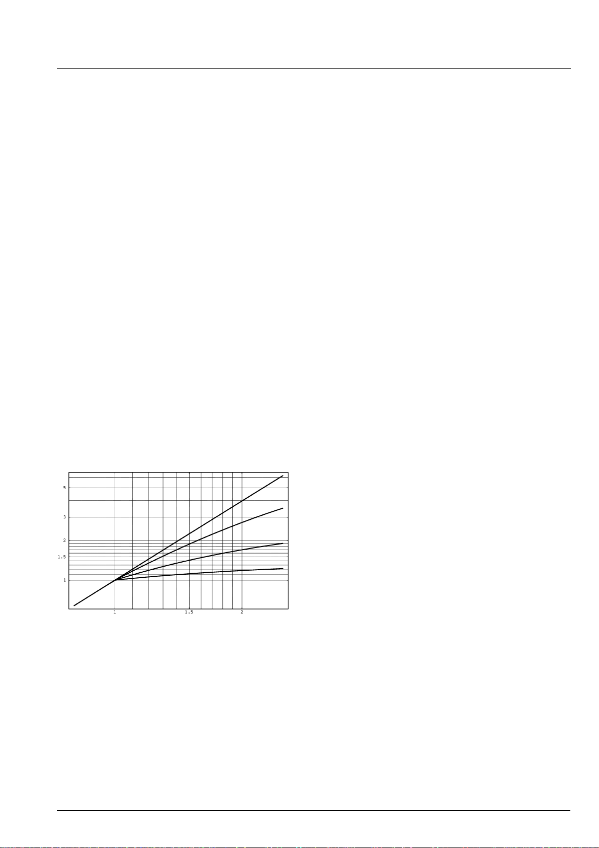
The average beam current limiter (BCL) uses the
SENSE input for the beam current measurement. The
BCL uses a different filter to average the beam current
during the active picture. The filter bandwidth is
approx. 2 kHz. The beam current limiter has an automatic offset adjustment that is active two lines before
the first cutoff measurement line.
The beam current limiter function is located in the
front-end. The data exchange between the front-end
and the back-end is done via a single-wire serial interface.
The beam current limiter allows the setting of a threshold current. If the beam current is above the threshold,
the excess current is low-pass filtered and used to
attenuate the RGB outputs by adjusting the white-drive
multipliers for the internal (digital) RGB signals, and
the analog contrast multipliers for the analog RGB
inputs, respectively. The lower limit of the attenuator is
programmable, thus a minimum contrast can always
be set. During the tube measurement, the ABL attenuation is switched off. After the white-drive measurement line it takes 3 lines to switch back to BCL limited
drives and brightness.
Typical characteristics of the ABL for different loop
gains are shown in Fig. 2–22; for this example the tube
has been assumed to have square law characteristics.
2.11.4.Analog RGB Insertion
The VCT 38xxA allows insertion of external analog
RGB signals. The RGB signal is key-clamped and
inserted into the main RGB by the Fast-Blank switch.
The external RGB input can be overlaid or underlaid to
the digital picture. The external RGB signals can be
adjusted independently as regards DC level (brightness) and magnitude (contrast).
All signals for analog RGB insertion (RIN, GIN, BIN,
FBLIN) must be synchronized to the horizontal flyback,
otherwise a horizontal jitter will be visible. The
VCT 38xxA has no means for timing correction of the
analog RGB input signals.
2.11.5.Fast-Blank Monitor
The presence of external analog RGB sources can be
detected by means of a Fast-Blank monitor. The status
of the Fast-Blank input can be monitored via an I
2
bus register. There is a 2 bit information, giving static
and dynamic indication of a Fast-Blank signal. The
static bit is directly reading the Fast-Blank input line,
whereas the dynamic bit is reading the status of a
flip-flop triggered by the negative edge of the FastBlank signal.
With this monitor logic it is possible to detect if there is
an external RGB source active and if it is a full screen
insertion or only a box. The monitor logic is connected
directly to the FBLIN pin.
C
Fig. 2–22: Beam current limiter characteristics:
beam current output vs. drive
BCL threshold: 1
Micronas 27
Page 28
VCT 38xxA ADVANCE INFORMATION
digital
SVM in
digital
R in
digital
G in
digital
B in
8
10
10
10
8-bit
DAC
SVM
1.88 mA
10-bit
DAC
Video
3.75 mA
10-bit
DAC
Video
3.75 mA
10-bit
DAC
Video
3.75 mA
white drive R
int. brightness *
white drive G
int. brightness *
int. brightness *
white drive B
0.94 mA
9-bit
DAC
1.5 mA
9-bit
DAC
1.5 mA
9-bit
DAC
1.5 mA
cutoff R
cutoff G
cutoff B
9-bit
DAC
2.2 mA
9 bit
DAC
2.2 mA
9 bit
DAC
2.2 mA
blanking
750
µA
blanking
µA
750
blanking
750
µA
analog
SVM out
analog
R out
analog
G out
analog
B out
serial interface
white drive R
white drive G
white drive B
int . brightness
ext. contrast
ext. brightness
ext. contrast *
white drive R *
key
Fig. 2–23: Video back-end
beam current lim.
ext. brightness *
white drive R
9-bit
DAC
1.5 mA
9-bit
U/I-DAC
3.75 mA
clamp
analog
R in
9-bit
DAC
1.5 mA
white drive G
ext. brightness *
9-bit
U/I-DAC
3.75 mA
ext. contrast *
white drive G *
beam current lim.
clamp clamp
analog
G in
ext. contrast *
white drive B *
ext. brightness *
beam current lim.
white drive B
9-bit
DAC
1.5 mA
9-bit
U/I-DAC
3.75 mA
analog
B in
fast
blank in
HV
blank &
measurem.
timing
8 bit
ADC
measurm.
SENSE
Input
measurement
I/O
buffer
28 Micronas
Page 29

ADVANCE INFORMATION VCT 38xxA
2.12.Synchronization and Deflection
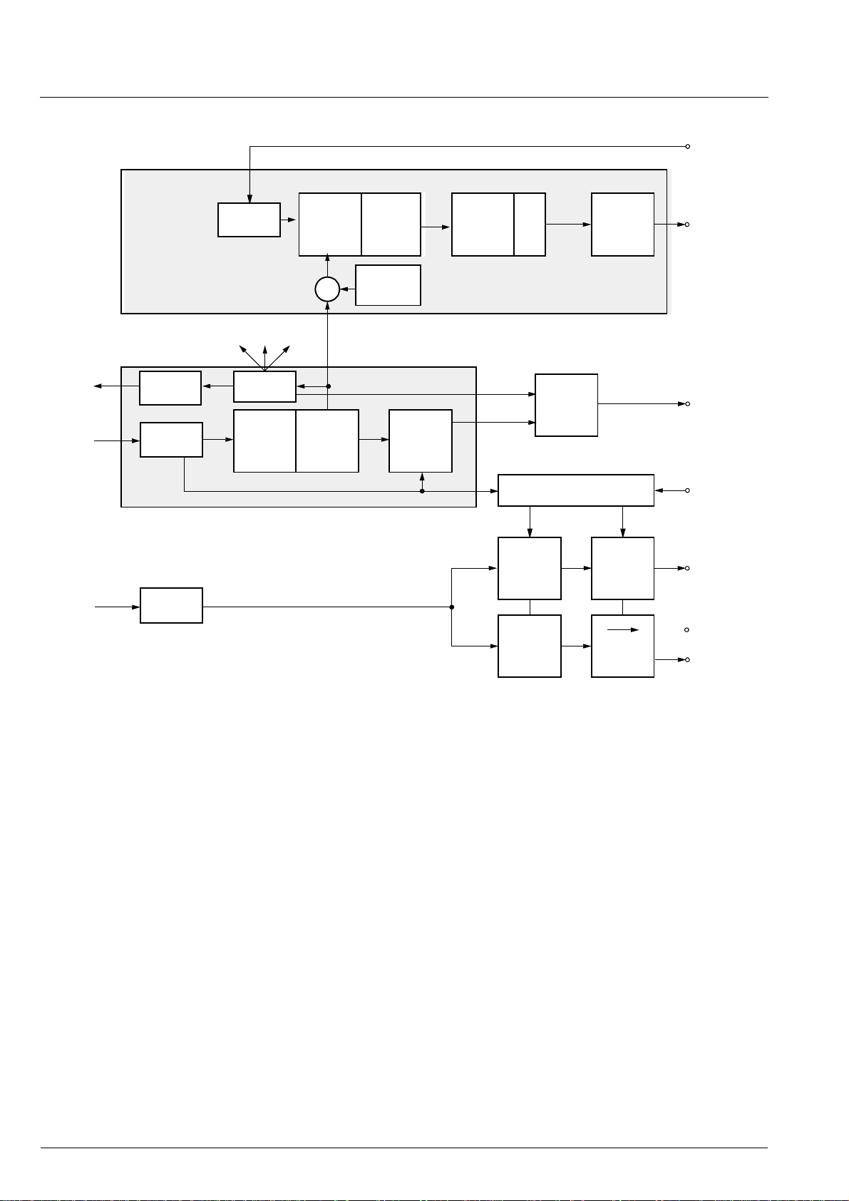
The synchronization and deflection processing is distributed over front-end and back-end. The video
clamping, horizontal and vertical sync separation and
all video related timing information are processed in
the front-end. Most of the processing that runs at the
horizontal frequency is programmed on the internal
Fast Processor (FP). Also the values for vertical and
East/West deflection are calculated by the FP software.
The generation of horizontal and vertical drive signals
can be synchronized to the video timing extracted in
the front-end or to a free running line counter in the
back-end.
2.12.1.Deflection Processing
The deflection processing generates the signals for the
horizontal and vertical drive (see Fig. 2–24). This block
contains two phase-locked loops:
– PLL2 generates the horizontal and vertical timing,
e.g. blanking, clamping and composite sync. Phase
and frequency are synchronized by the front sync
signal.
– PLL3 adjusts the phase of the horizontal drive pulse
and compensates for the delay of the horizontal output stage. Phase and frequency are synchronized
by the oscillator signal of PLL2.
2.12.3.Horizontal Phase Adjustment
This section describes a simple way to align PLL
phases and the horizontal frame position.
1. With HDRV the duration of the horizontal drive pulse
has to be adjusted
2. With POFS2 the delay between input video and display timing (e.g. clamping pulse for analog RGB)
has to be adjusted
3. With CSYDEL the delay between video and analog
RGB (OSD) has to be adjusted.
4. With CSYDEL and HPOS the horizontal position of
both, the digital and analog RGB signal (from
SCART) relative to the clamping pulse has to be
adjusted to the correct position, e.g. the pedestal of
the generator signal.
5. With POFS3 the position of horizontal drive/flyback
relative to RGB has to be adjusted
6. With NEWLIN the position of a scaled video picture
can be adjusted (left, middle, center, etc; versions
with panorama scaler only).
7. With HBST and HBSO, the start and stop values for
the horizontal blanking have to be adjusted.
Note: The processing delay of the internal digital video
path differs depending on the comb filter option of the
VCT 38xxA. The versions with comb filter have an
additional delay of 34 clock cycles.
The horizontal drive circuitry uses a digital sine wave
generator to produce the exact (subclock) timing for
the drive pulse HOUT. The generator runs at 1 MHz.
Under control of the EHPLL bit and the internal voltage
supervision it is either synchronized by the deflection
PLL or it is free running. In the output stage the frequency is divided down to give drive-pulse period and
width. The drive pulse width is programmable. The
horizontal drive uses an open drain output transistor.
After power on or during reset the HOUT generation is
switched to a free running mode with a fix duty cycle of
50 %. For normal operation the EHPLL bit has to be
set first. During the switch the actual period of HOUT
can vary by up to 1
2.12.2.Angle and Bow Correction
The Angle and Bow correction is part of the horizontal
drive PLL. This feature allows a shift of the horizontal
drive pulse phase depending on the vertical position
on the screen. The phase correction has a linear
(angle) and a quadratic term (bow).
µs.
Micronas 29
Page 30
VCT 38xxA ADVANCE INFORMATION
HFLB
PLL3
MSY
FSY
VDATA
Main
Sync
Generator
Front
Sync
Interface
Vertical
Data
Skew
Measure-
ment
blanking, clamping, etc.
Display
Timing
Phase
Comparator
Low-pass
Comparator
Low-pass
&
vertical reset
Phase
&
+
DCO
DCO
Angle &
Bow
PLL2
Line
Counter
Sinewave
Generator
DAC
&
LPF
Generation
Clock & Control
E/W
correction
Sawtooth
Sync
1:64
&
Output
Stage
PWM
15-bit
PWM
15-bit
HOUT
INTLC
VPROT
EW
VERT
VERTQ
Fig. 2–24: Deflection processing block diagram
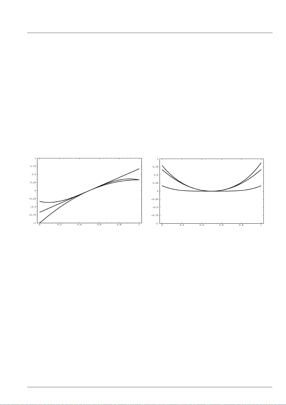
2.12.4.Vertical and East/West Deflection
The calculations of the vertical and East/West deflection waveforms is done by the internal Fast Processor
(FP). The algorithm uses a chain of accumulators to
generate the required polynomial waveforms. To produce the deflection waveforms, the accumulators are
initialized at the beginning of each field. The initialization values must be computed by the TV control processor and are written to the front-end once. The
waveforms are described as polynomials in x, where x
varies from 0 to 1 for one field.
P: a + b(x-0.5) + c(x-0.5)
2 +
d(x-0.5)3 + e(x-0.5)
4
The initialization values for the accumulators a0..a3 for
vertical deflection and a0..a4 for East/West deflection
are 12-bit values.
Fig. 2–25 shows several vertical and East/West deflection waveforms. The polynomial coefficients are also
stated.
In order to get a faster vertical retrace timing, the output impedance of the vertical D/A-converter can be
reduced by 50 % during the retrace.
2.12.5.EHT Compensation
The vertical waveform can be scaled according to the
average beam current. This is used to compensate the
effects of electric high-tension changes due to beam
current variations. EHT compensation for East/West
deflection is done with an offset corresponding to the
average beam current.
30 Micronas
Page 31
ADVANCE INFORMATION VCT 38xxA
2.12.6.Protection Circuitry
Picture tube and drive stage protection is provided
through the following measures:
– Vertical flyback protection input:
This pin searches for a negative edge in every field,
otherwise the RGB drive signals are blanked.
– Drive shutoff during flyback:
This feature can be selected by software.
– Safety input pin:
This input has two thresholds. Between zero and the
lower threshold, normal functioning takes place.
Between the lower and the higher threshold, the
RGB signals are blanked. Above the higher threshold, the RGB signals are blanked and the horizontal
drive is shut off. Both thresholds have a small hysteresis.
Vertical:
0,1,0,0
0,1,1,0
0,1,0,1
Fig. 2–25: Vertical and East/West deflection waveforms
2.13.Reset Function
Reset of all VDP functions is performed by the RESQ
pin. When this pin becomes active, all internal registers and counters are lost. The TV controller can activate the RESQ pin by software (see Section 5.7.2. on
page 90).
When the RESQ pin is released, the internal reset is
still active for 4
µs. After that time, the initialization of
all required registers is performed by the internal Fast
Processor. This takes approximately 60
initialization procedure it is not possible to access the
VDP via the I
2
C interface.
µs. During this
The VDP has clock and voltage supervision circuits to
generate a stable HOUT signal. The voltage supervision activates an internal reset signal when the supply
East/West:a,b,c,d
for the digital circuits (VSUP
a,b,c,d,e
0,0,1,0,0
0,0,0,0,1
0,0,1,1,1
) goes below ~2.5 V for
D
more than 50 ns. This reset signal is extended by
µs after VSUP
50
is back again.
D
2.14.Standby and Power-On
The VDP does not have a standby mode. To disable all
the analog and digital video functions, it is necessary
to switch off the supplies for analog front-end
(VSUP
circuitry (VSUP
), analog back-end (VSUPAB) and digital
AF
).
D
Micronas 31
Page 32
VCT 38xxA ADVANCE INFORMATION
2.15.I2C Bus Slave Interface
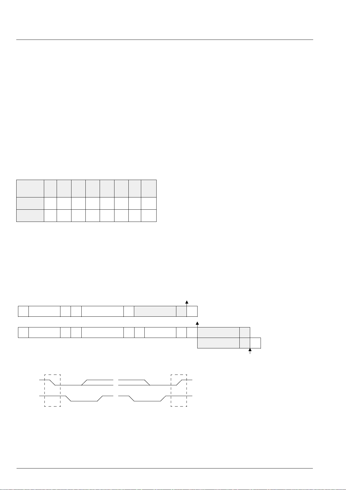
Communication between the VDP and the TV controller is done via I
2
I
C bus please refer to the Philips manual ‘I2C bus
2
C bus. For detailed information on the
Specification’.
2
The VDP has two I
ibility with VPC/DDP applications)
front-end and one in the back-end. Both I
faces use I
2
C clock synchronization to slow down the
interface if required. Both I
level of subaddress: the I
to address the VDP and a subaddress selects one of
the internal registers. The I
C bus slave interfaces (for compat-
− one in the
2
C bus inter-
2
C bus interfaces use one
2
C bus chip address is used
2
C bus chip addresses are
given below:
2
Table 2–2: I
Chip
Address
front-end
back-end
C chip addresses
A6 A5 A4 A3 A2 A1 A0 R/W
10001111/0
10001011/0
2
Fig. 2–26 shows I
C bus protocols for read and write
operations of the interface; the read operation requires
an extra start condition and repetition of the chip
address with read command set.
2.15.1.Control and Status Registers
Tabl e 2 –3 gives definitions of the VDP control and status registers. The number of bits indicated for each
register in the table is the number of bits implemented
in hardware, i.e. a 9-bit register must always be
accessed using two data bytes but the 7 MSB will be
‘don’t care’ on write operations and ‘0’ on read operations. Write registers that can be read back are indicated in Table 2–3.
Functions implemented by software in the on-chip control microprocessor (FP) are explained in Table 2–5.
A hardware reset initializes all control registers to 0.
The automatic chip initialization loads a selected set of
registers with the default values given in Table 2–3.
The register modes given in Table 2–3 are
– w: write only register
The registers of the VDP have 8 or 16-bit data size;
16-bit registers are accessed by reading/writing two
8-bit data words.
SS1000 111
1000 111
SDA
SCL
WAck
AckW 0111 1100
0111 1100
AckS1 or 2 byte Data
Ack
1
0
1000 111 R high byte Data
– w/r: write/read data register
– r: read data from VDP
– v: register is latched with vertical sync
– h: register is latched with horizontal
P
I2C write access
subaddress 7c
2
I
Ack
low byte Data
W
R
PS
Ack
Nak
S
P
Nak P
=
=
=
=
=
=
C read access
subaddress 7c
0
1
0
1
Start
Stop
2
Fig. 2–26: I
C bus protocols
32 Micronas
Page 33

ADVANCE INFORMATION VCT 38xxA
Table 2–3: I2C control and status registers of the video front-end
I2C Sub
address
Number
of bits
Mode Function Default Name
FP Interface
h’35 8 r FP status
bit [0] write request
bit [1] read request
bit [2] busy
h’36 16 w bit[8:0] 9-bit FP read address
bit[11:9] reserved, set to zero
h’37 16 w bit[8:0] 9-bit FP write address
bit[11:9] reserved, set to zero
h’38 16 w/r bit[11:0] FP data register, reading/writing to this
register will autoincrement the FP read/
write address. Only 16 bit of data are
transferred per I
2
C telegram.
Black Line Detector
h’12 16 r read only register, do not write to this register!
after reading, LOWLIN and UPLIN are reset to 127 to start a
new measurement
bit[6:0] number of lower black lines
bit[7] always 0
bit[14:8] number of upper black lines
bit[15] normal/black picture
FPSTA
FPRD
FPWR
FPDAT
BLKLIN
LOWLIN
UPLIN
BLKPIC
Miscellaneous
h’29 16 w/r Test pattern generator:
bit[10:0] reserved (set to 0)
bit[11] 0/1 disable/enable test pattern generator
bit[13:12] output mode:
00 Y/C = ramp (240 ... 17)
01 Y/C = 16
10 Y/C = 90
11 Y/C = 240
bit[15:14] 0/1 reserved (set to 0)
h’22 16 w/r NEWLINE (available for versions with panorama scaler only):
bit[10:0] NEWLINE register
This register defines the readout start of
the next line in respect to the value of the
sync counter.
bit [15:11] reserved (set to 0)
TPG
0
TPGEN
0
TPGMODE
0
0
NEWLIN
0
Micronas 33
Page 34

VCT 38xxA ADVANCE INFORMATION
Table 2–4: I2C control and status registers of the video back-end
I2C Sub
address
Number
of bits
Mode Function Default Name
1)
priority mask register
If bit[x] is set to 1 then the function is active for the respective signal priority
Luminance Channel
h’61 9 w v bit [5:0] 0..63/32 main picture contrast 32 CTM
h’65 9 w v bit [5:0] 0..63/32 side picture contrast 32 CTS
h’51 9 w v bit [8:0]
h’55 9 w v bit [8:0]
h’75 9 w v luma channel, priority mask register
−256..255 main picture brightness 0 BRM
−256..255 side picture brightness 0 BRS
0PBCT
bit [7:0] 0/1 select contrast, brightness, matrix
for main/side picture
h’71 9 w v luma channel, priority mask register
PBERGB
0
bit [7:0] 0/1 select main (video) / external (via CLUT)
RGB
Black-Level Expander
h’59 9 w v black-level expander
bit [3:0] 0..15 tilt coefficient
bit [8:4] 0...31 amount
12
8
BLE1
BTLT
BAM
1)
1)
h’5d 9 w v black-level expander, threshold:
bit [8:0] 0..511 disable expansion, threshold value 200
h’73 9 w v black-level expander, measurement
bit[0] 0/1 50/60 Hz measurement windowlength
bit [8:1] 0..255 vstart/2
start line = vstart
stop line = 336/283
− vstart
or vertical blanking
h’7d 9 w v black-level expander, priority mask register
bit [7:0] 0/1 enable/disable black-level expander
Dynamic Peaking
h’69 9 w v luma peaking filter, the gain at high frequencies and small signal
amplitudes is: 1 + (k1+k2)/8
bit [3:0] 0..15 k1: peaking level undershoot
bit [7:4] 0..15 k2: peaking level overshoot
bit [8] 0/1 peaking value normal/inverted
(peaking/softening)
h’6d 9 w v luma peaking filter, coring
bit [4:0] 0..31 coring level
bit [7:5] reserved
bit [8] 0/1 peaking filter center frequency high/
low
BLE2
BTHR
BLE3
0
BWL
15
BVST
0PBBLE
PK1
4
PKUN
4
PKOV
0
PKINV
PK2
3
COR
0
PFS
1)
h’79 9 w v luma peaking filter, priority mask register
0 PBPK
1)
bit [7:0] 0/1 disable/enable peaking transient
suppression when signal is switched
34 Micronas
Page 35

ADVANCE INFORMATION VCT 38xxA
I2C Sub
address
Number
of bits
Mode Function Default Name
Soft Limiter
h’41 9 w v luma soft limiter, slope A and B
bit [3:0] slope segment A
bit [7:4] slope segment B
h’45 9 w v luma soft limiter, absolute limit
bit [7:0] luma soft limiter absolute limit
255
0
0
LSL1
LSLSA
LSLSB
LSL2
LSLAL
(unsigned)
bit [8] 0/1 modulation off/on
1
LSLM
h’49 9 w v bit [8:0] luma soft limiter segment B tilt point (unsigned) 300 LSLTB
h’4d 9 w v bit [8:0] luma soft limiter segment A tilt point (unsigned) 250 LSLTA
Chrominance Channel
h’14 8 w/r luma/chroma matching
bit [2:0]
−3...3 variable chroma delay
0
LCM
CDEL
bit [7:3] reserved, set to 0
h’5e 9 w v digital transient improvement
bit [3:0] 0..15 coring value
bit [7:4] 0..15 DTI gain
bit [8] 0/1 narrow/wide bandwidth mode
1
5
1
DTI
DTICO
DTIGA
DTIMO
h’7c
h’74
h’6c
h’64
h’5c
h’54
h’78
h’70
h’68
h’60
h’58
h’50
Inverse Matrix
main picture matrix coefficient R
9
9
w v
w v
bit [8:0] −256/128 ... 255/128
bit [8:0]
−256/128 ... 255/128
main picture matrix coefficient G
9
9
w v
w v
bit [8:0] −256/128 ... 255/128
bit [8:0]
−256/128 ... 255/128
main picture matrix coefficient B
9
9
w v
w v
bit [8:0] −256/128 ... 255/128
bit [8:0]
−256/128 ... 255/128
side picture matrix coefficient R
9
9
w v
w v
bit [8:0] −256/128 ... 255/128
bit [8:0]
−256/128 ... 255/128
side picture matrix coefficient G
9
9
w v
w v
bit [8:0] −256/128 ... 255/128
bit [8:0]
−256/128 ... 255/128
side picture matrix coefficient B
9
9
w v
w v
bit [8:0] −256/128 ... 255/128
bit [8:0]
−256/128 ... 255/128
−Y = MR1M*C
−Y = MG1M*C
−Y = MB1M*C
−Y = MR1S*C
−Y = MG1S*C
−Y = MB1S*C
+ MR2M*C
B
+ MG2M*C
B
+ MB2M*C
B
+ MR2S*C
B
+ MG2S*C
B
+ MB2S*C
B
R
086MR1M,
MR2M
R
R
−22
−44
MG1M,
MG2M
1130MB1M,
MB2M
R
073MR1S,
MR2S
R
R
−19
−37
MG1S,
MG2S
970MB1S,
MB2S
Micronas 35
Page 36

VCT 38xxA ADVANCE INFORMATION
I2C Sub
address
Number
of bits
Mode Function Default Name
Color Lookup Table
h’00
h’0f
16 w h color look-up table : 16 entries, 12 bit wide,
−
The CLUT registers are initialized at power-up
bit [3:0] 0..15 blue amplitude
bit [7:4] 0..15 green amplitude
bit [11:8] 0..15 red amplitude
h’4c 9 w v digital OSD insertion contrast for R (amplitude range: 0 to 255)
bit [3:0] 0..13 R amplitude = CLUTn
⋅ (DRCT + 4)
14,15 invalid
picture frame insertion contrast for R (ampl. range: 0 to 255)
bit [7:4] 0..13 R amplitude = PFCR
⋅ (PFRCT + 4)
14,15 invalid
000h
f00h
0f0h
ff0h
00fh
f0fh
0ffh
fffh
7ffh
700h
070h
770h
007h
707h
077h
777h
8
8
CLUT0
CLUT15
RCT
DRCT
PFRCT
h’48 9 w v digital OSD insertion contrast for G (amplitude range: 0 to 255)
bit [3:0] 0..13 G amplitude = CLUTn
⋅ (DGCT + 4)
14,15 invalid
picture frame insertion contrast for G (ampl. range: 0 to 255)
bit [7:4] 0..13 G amplitude = PFCG
⋅ (PFGCT + 4)
14,15 invalid
h’44 9 w v digital OSD insertion contrast for B (amplitude range: 0 to 255)
bit [3:0] 0..13 B amplitude = CLUTn
⋅ (DBCT + 4)
14,15 invalid
picture frame insertion contrast for B (ampl. range: 0 to 255)
bit [7:4] 0..13 B amplitude = PFCB
⋅ (PFBCT + 4)
14,15 invalid
Picture Frame Generator
h’11 16 w h picture frame color
bit [3:0] 0..15 blue amplitude
bit [7:4] 0..15 green amplitude
bit [11:8] 0..15 red amplitude
h’47 9 w v bit [2:0] picture frame generator priority id
bit [8] enable prio id for picture frame generator
h’4F 9 w v bit [8:0] horizontal picture frame begin
code 0 = picture frame generator horizontally disabled
code 1FF = full frame
GCT
DGCT
8
PFGCT
8
BCT
8
DBCT
8
PFBCT
PFC
0
PFCB
0
PFCG
0
PFCR
0PFGID
PFGEN
0PFGHB
h’53 9 w v bit [8:0] horizontal picture frame end 0 PFGHE
h’63 9 w v bit [8:0] vertical picture frame begin
270 PFGVB
code 0 = picture frame generator vertically disabled
h’6f 9 w v bit [8:0] vertical picture frame end 56 PFGVE
36 Micronas
Page 37

ADVANCE INFORMATION VCT 38xxA
I2C Sub
address
Number
of bits
Mode Function Default Name
Scan Velocity Modulation
h’5a 9 w v video mode coefficients
bit [5:0] gain1
bit [8:6] differentiator delay 1 (0= filter off, 1...6= delay)
h’56 9 w v text mode coefficients
bit [5:0] gain 2
bit [8:6] differentiator delay 2 (0= filter off, 1...6= delay)
h’52 9 w v limiter
bit [6:0] limit value
bit [8:5] not used, set to “0”
h’4e 9 w v delay and coring
bit [3:0] adjustable delay, in 1/2 display clock steps,
(value 5 : delay of SVMOUT is the same as for
RGBOUT
bit [7:4] coring value
bit [8] not used, set to “0”
Display Controls
h’4a
h’46
h’42
9
9
9
w v
w v
w v
cutoff Red
cutoff Green
cutoff Blue
60
60
100
4
4
0
7
0
0
0
0
SVM1
SVG1
SVD1
SVM2
SVG2
SVD2
SVM3
SVLIM
SVM4
SVDEL
SVCOR
CR
CG
CB
Tube- and Picture-Measurements
h’7b 9 w v picture measurement start line
bit [8:0] (TML+9)..511 first line of picture measurement 23
h’6b 9 w v picture measurement stop line
bit [8:0] (PMST+1)..511 last line of picture measurement 308
h’7f 9 w v tube measurement line
bit [8:0] 0..511 start line for tube measurement 15
h’25 8 w/r tube and picture measurement control
bit [0] 0/1 disable/enable tube measurement
bit [1] 0/1 80/40 kHz bandwidth for
picture measurement
bit [2] 0/1 disable/enable picture measurement
(writing a ’1’ starts one measurement
cycle)
bit [3] 0/1 large/small picture measurement window,
will be disabled from bit[3] in address h’32
bit [4] 0/1 measure / offset check for adc
bit [7:5] reserved
h’13 16 w/r white drive measurement control
bit [9:0] 0..1023 RGB values for white drive beam current
measurement
bit [10] reserved
bit [11] 0/1 RGB values for white drive beam current
measurement disabled/enabled
PMST
PMSO
TML
0TPM
TMEN
PMBW
PMEN
PMWIN
OFSEN
WDM
WDRV
512
EWDM
0
Micronas 37
Page 38

VCT 38xxA ADVANCE INFORMATION
I2C Sub
address
Number
of bits
Mode Function Default Name
8 r measurement result registers
h’18
h’19
h’1a
h’1d
h’1c
h’1b
minimum in active picture
maximum in active picture
white drive
cutoff/leakage red
cutoff/leakage green
cutoff/leakage blue,
read pulse starts tube measurement
h’1e 8 r measurement adc status and Fast-Blank input status
measurement status register
bit [0] 0/1 tube measurement active / complete
bit [2:1] white drive measurement cycle
00 red
01 green
10 blue
11 reserved
bit [3] 0/1 picture measurement active / complete
bit [4] 0/1 Fast-Blank input Low / High (static)
bit [5] 1 Fast-Blank input negative transition since
last read (bit reset at read)
bit [7:6] reserved
−
MRMIN
MRMAX
MRWDR
MRCR
MRCG
MRCB
− PMS
Vertical Timing
h’67 9 w v vertical blanking start
bit [8:0] 0..511 first line of vertical blanking 305
h’77 9 w v vertical blanking stop
bit [8:0] 0..511 last line of vertical blanking 25
h’5f 9 w v vertical free run period
bit [8:0] free running field period = (value+4) lines 309
Horizontal Deflection and Timing
h’7a 9 w v quadratic term of angle & bow correction
bit [8:0]
−256..+255 (± 500 ns)
h’76 9 w v linear term of angle & bow correction
bit [8:0]
−256..+255 (± 500 ns)
h’6e 9 w v adjustable delay of PLL2, clamping, and blanking (relative to
front sync)
adjust clamping pulse for analog RGB input
bit [8:0]
−256..+255 (± 8 µs)
h’72 9 w v adjustable delay of flyback, main sync, csync and analog RGB
(relative to PLL2)
adjust horizontal drive or csync
bit [8:0]
−256..+255 (± 8 µs)
VBST
VBSO
VPER
0BOW
0ANGLE
−141 POFS2
0POFS3
h’7e 9 w v adjustable delay of main sync (relative to flyback)
120 HPOS
adjust horizontal position for digital picture
bit [8:0] 20 steps=1
h’5b 9 w v start of horizontal blanking
µs
1 HBST
bit [8:0] 0..511
38 Micronas
Page 39

ADVANCE INFORMATION VCT 38xxA
I2C Sub
address
Number
of bits
Mode Function Default Name
h’57 9 w v end of horizontal blanking
bit [8:0] 0..511
h’62
h’66
h’6a
PLL2/3 filter coefficients, 1of5 bit code (n+ set bit number)
9
9
9
w v
w v
w v
bit [5:0] proportional coefficient PLL3, 2
bit [5:0] proportional coefficient PLL2, 2
bit [5:0] integral coefficient PLL2, 2
−n−1
−n−1
−n−5
h’15 16 w/r horizontal drive and vertical signal control register
bit [5:0] 0..63 horizontal drive pulse duration in
(internally limited to 4..61)
bit [6] 0/1 disable/enable horizontal PLL2 and PLL3
bit [7] 0/1 1: disable horizontal drive pulse during
flyback
bit [8] reserved, set to ’0’
bit [9] 0/1 enable/disable ultra black blanking
bit [10] 0/1 0: all outputs blanked
1: normal mode
bit [11] 0/1 enable/disable clamping for analog RGB
input
bit [12] 0/1 disable/enable vertical free running mode
(FIELD is set to field2, no interlace)
bit [13] 0/1 enable/disable vertical protection
bit [14] reserved, set to ’0’
bit [15] 0/1 disable/enable phase shift of display clock
µs
48 HBSO
2
PKP3
1
PKP2
2
PKI2
HVC
32
HDRV
0
EHPLL
0
EFLB
0
0
DUBL
1
EBL
0
DCRGB
0
SELFT
0
DVPR
0
1
DISKA
h’9d 8 w/r sync output control
bit [0] invert INTLC
bit [4:1] reserved, set to ’0’
bit [5] force INTLC to polarity defined in ‘INTLCINV’
Miscellaneous
h’32 8 w/r Fast-Blank interface mode
bit [0] 0 internal Fast-Blank from FBLIN pin
1 force internal Fast-Blank signal to High
bit [1] 0/1 internal Fast-Blank active High/Low
bit [2] 0/1 disable/enable clamping reference for
RGB outputs
bit [3] 1 full line MADC measurement window,
disables bit [3] in address h’25
bit [4] 0/1 horizontal flyback input active High/Low
bit [6:5] reserved (set to 0)
bit [7] vertical output select
0 VERTQ output
1 INTLC output
h’4b 9 w v Fast-Blank input, priority mask register
bit [7:0] 0/1 disable/enable analog Fast-Blank input
0SYCTRL
INTLCINV
INTLCFO
0FBMOD
FBFOH
FBPOL
CLMPR
FLMW
FLPOL
VOS
0PBFB
1)
Micronas 39
Page 40

VCT 38xxA ADVANCE INFORMATION
Table 2–5: Control registers of the Fast Processor for control of the video front-end functions
− default values are initializied at reset
FP Subaddress
h’20 Standard select:
Function Default Name
bit[2:0] standard
0 PAL B,G,H,I (50 Hz) 4.433618
1 NTSC M (60 Hz) 3.579545
2 SECAM (50 Hz) 4.286
3 NTSC44 (60 Hz) 4.433618
4 PAL M (60 Hz) 3.575611
5 PAL N (50 Hz) 3.582056
6 PAL 60 (60 Hz) 4.433618
7 NTSC COMB (60 Hz) 3.579545
bit[3] 0/1 standard modifier
bit[4] reserved (set to 0)
bit[5] 0/1 2-H comb filter off/on
bit[6] 0/1 S-VHS mode off/on (2-H comb is switched off)
Option bits allow to suppress parts of the initialization, this can be used
for color standard search:
Standard Selection
0SDT
PAL
NTSC
SECAM
NTSC44
PALM
PALN
PAL60
NTSCC
SDTMOD
PAL modified to simple PAL
NTSC modified to compensated NTSC
SECAM modified to monochrome 625
NTSCC modified to monochrome 525
COMB
SVHS
SDTOPT
bit[7] no hpll setup
bit[8] no vertical setup
bit[9] no acc setup
bit[10] 2-H comb filter set-up only
bit[11] status bit, normally write 0. After the FP has switched to a
new standard, this bit is set to 1 to indicate operation
complete. Standard is automatically initialized when the
insel register is written.
h’148 Enable automatic standard recognition (ASR)
bit[0] 0/1 PAL B,G,H,I (50 Hz) 4.433618
bit[1] 0/1 NTSC M (60 Hz) 3.579545
bit[2] 0/1 SECAM (50 Hz) 4.286
bit[3] 0/1 NTSC44 (60 Hz) 4.433618
bit[4] 0/1 PAL M (60 Hz) 3.575611
bit[5] 0/1 PAL N (50 Hz) 3.582056
bit[6] 0/1 PAL 60 (60 Hz) 4.433618
bit[10:7] reserved set to 0
bit[11] 1 reset status information ‘switch’ in asr_status
(cleared automatically)
0: disable recognition; 1: enable recognition
Note: For correct operation don’t change FP reg. 20h and 21h, while
ASR is enabled!
0ASR_ENA
40 Micronas
Page 41

ADVANCE INFORMATION VCT 38xxA
FP Subaddress
Function Default Name
h’14e Status of automatic standard recognition
bit[0] 1 error of the vertical standard (neither 50 nor 60 Hz)
bit[1] 1 detected standard is disabled
bit[2] 1 search active
bit[3] 1 search terminated, but failed
bit[4] 1 no color found
bit[5] 1 standard has been switched (since last reset of this
flag with bit[11] of asr_enable)
bit[4:0]
00000 all ok
00001 search not started, because vwin error detected
(no input or SECAM L)
00010 search not started, because detected vert. standard
not enabled
0x1x0 search started and still active
01x00 search failed (found standard not correct)
01x10 search failed, (detected color standard not enabled)
10000 no color found (monochrome input or switch betw.
CVBS/SVHS necessary)
h’21 Input select: writing to this register will also initialize the standard
bit[1:0] luma selector
00 VIN1
01 VIN2
10 VIN3
11 VIN4
bit[2] chroma selector
0CIN1
1CIN2
bit[4:3] IF compensation
00 off
01 6 dB/Okt
10 12 dB/Okt
11 10 dB/MHz only for SECAM
bit[6:5] chroma bandwidth selector
00 narrow
01 normal
10 broad
11 wide
bit[7] 0/1 adaptive/fixed SECAM notch filter
bit[8] 0/1 enable luma lowpass filter
bit[10:9] hpll speed
00 no change
01 terrestrial
10 vcr
11 mixed
bit[11] status bit, write 0, this bit is set to 1 to indicate
operation complete.
0 ASR_STATUS
VWINERR
DISABLED
BUSY
FAILED
NOCOLOR
SWITCH
INSEL
00
VIS
0
CIS
00
IFC
01
CBW
FNTCH
LOWP
HPLLMD
h’22 Available for versions with panorama scaler only!
0SFIF
picture start position, this register sets the start point of active video,
this can be used e.g. for panning. The setting is updated when ’sdt’
register is updated.
h’23 luma/chroma delay adjust. The setting is updated when ’sdt’ register is
0LDLY
updated.
bit[5:0] reserved, set to zero
bit[11:6] luma delay in clocks, allowed range is +1 ...
−7
Micronas 41
Page 42

VCT 38xxA ADVANCE INFORMATION
FP Subaddress
Function Default Name
h’2f YCrCb mode control register
bit[6:0] reserved (set to 0)
bit[7] 1 ADC over-/underflow
(has to be reset after read if used)
bit[8] 0 disable/enable YC
bit[9] ADC range
0 nominal input amplitude (
1 extented input amplitude (
bit[11:10] reserved (set to 0)
Note: Activate the YC
− enabling YC
rCb
mode by
rCb
− selecting simple PAL or NTSC M, svhs=1, comb=0 in the std register
− setting cbw=2 in the insel register
h’27 comb filter control register
bit[0] 0 comb coefficients are calculated for luma/chroma
1 comb coefficients for luma are used for luma and
chroma
bit[1] 0 luma comb strength depends on signal amplitude
1 luma comb strength is independent of amplitude
bit[2] 0 reduced comb booster
1 max comb booster
bit[4:3] 0..3 comb strength for chroma signal
bit[6:5] 0..3 comb strength for luma signal
bit[11:7] 0..31 overall limitation of the calculated comb coefficients
0 no limitation
31 max limitation (1/2)
rCb
±350 mV)
±500 mV)
Comb Filter
0YC
rCb
CMB_UC
0
CC
0
DAA
1
KB
3
KC
2
KY
0
CLIM
Color Processing
h’30
Saturation control
2070 ACC_SAT
bit[11:0] 0...4094 (2070 corresponds to 100% saturation)
4095 disabled (test mode only)
h’39 amplitude killer level (0:killer disabled) 25 KILVL
h’3a amplitude killer hysteresis 5 KILHY
h’dc NTSC tint angle,
±512 = ±π/4 0 TINT
DVCO
h’f8 crystal oscillator center frequency adjust,
h’f9 crystal oscillator center frequency adjustment value for line-lock mode
True adjust value is DVCO
− ADJUST. For factory crystal alignment,
−2048 ... 2047 −720 DVCO
read only ADJUST
using standard video signal: set DVCO = 0, set lock mode, read crystal
offset from ADJUST register and use negative value for initial center
frequency adjustment via DVCO.
h’f7 crystal oscillator line-locked mode, lock command/status
0XLCK
write: 100 enable lock
0 disable lock
read: 0 unlocked
>2047 locked
h’b5 crystal oscillator line-locked mode, autolock feature. If autolock is
400 AUTOLOCK
enabled, crystal oscillator locking is started automatically.
bit[11:0] threshold; 0: autolock off
42 Micronas
Page 43

ADVANCE INFORMATION VCT 38xxA
FP Subaddress
h’12
Function Default Name
general purpose control bits
bit[2:0] reserved, do not change
bit[3] vertical standard force
bit[8:4] reserved, do not change
bit[9] disable flywheel interlace
bit[11:10] reserved, do not change
to enable vertical free run mode set vfrc to 1 and dflw to 0
h’13 standard recognition status
bit[0] 1 vertical lock
bit[1] 1 horizontally locked
bit[2] no signal detected
bit[3] 1 color amplitude killer active
bit[4] 1 disable amplitude killer
bit[5] 1 color ident killer active
bit[6] 1 disable ident killer
bit[7] 1 interlace detected
bit[8] 1 no vertical sync detection
bit[9] 1 spurious vertical sync detection
bit[11:10] reserved
h’14
input noise level read only NOISE
FP Status
GPC
0
VFRC
1
DFLW
− ASR
h’cb number of lines per field, P/S: 312, N: 262 read only NLPF
h’15 vertical field counter, incremented per field VCNT
h’74 measured sync amplitude value, nominal: 768 (PAL), 732 (NTSC) read only SAMPL
h’36 measured burst amplitude read only BAMPL
h’f0 firmware version number
read only SW_VERSION
bit[7:0] internal revision number
bit[11:8] firmware release
h’170
status of macrovision detection
read only MCV_STATUS
bit[0] AGC pulse detected
bit[1] pseudo sync detected
h’171
h’172
bit[11:0] first line of macrovision detection window 6 MCV_START
bit[11:0] last line of macrovision detection window 15 MCV_STOP
Horizontal Scaler
1)
these registers are updated when the scaler mode register is written
h’40 scaler mode register
bit[1:0] scaler mode
0SCMODE
MODE
0 linear scaling mode
1 nonlinear scaling mode, ’panorama’
2 nonlinear scaling mode, ’waterglass’
3 reserved
bit[10:2] reserved, set to 0
bit[11] scaler update
SCUP
0 start scaler update command,
when the registers are updated the bit is set to 1
Micronas 43
Page 44
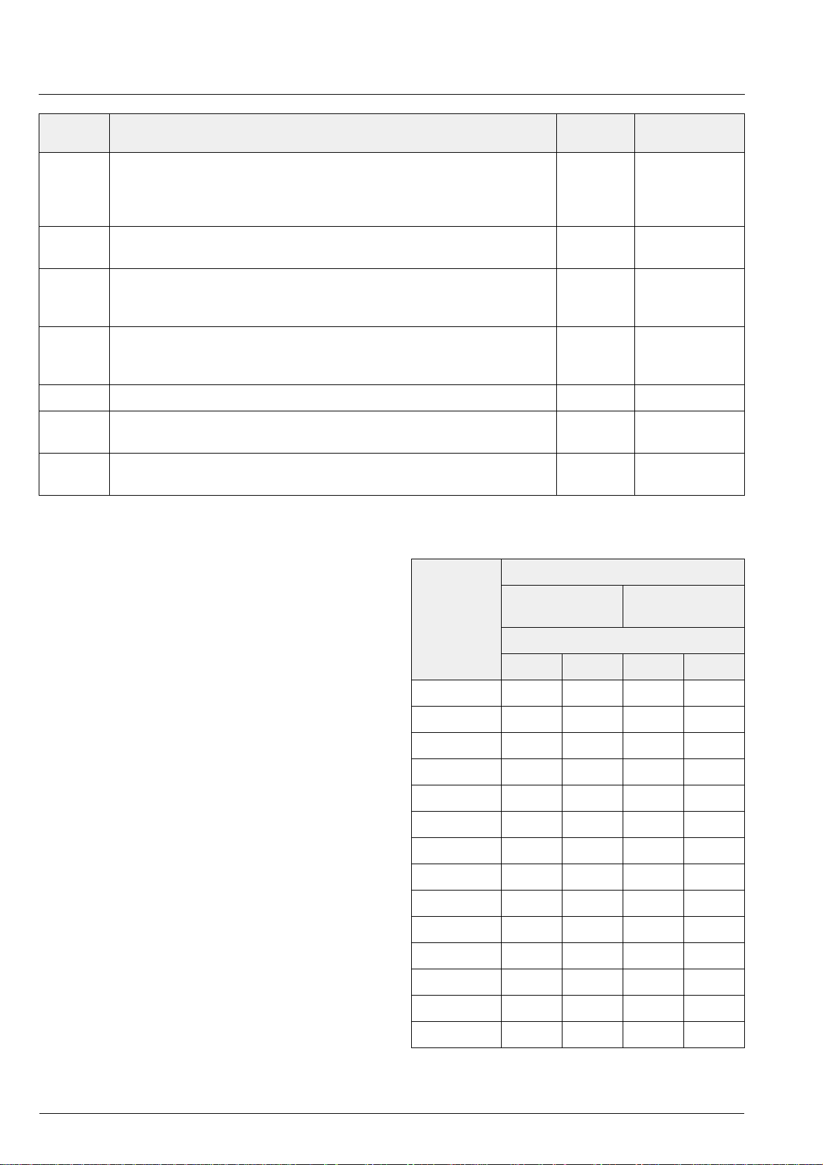
VCT 38xxA ADVANCE INFORMATION
FP Subaddress
h’41 luma offset register
Function Default Name
1)
bit[6:0] luma offset 0..127
ITU-R output format: 57
CVBS output format: 4
h’42 active video length for 1-h FIFO
1)
bit[11:0] length in pixels
h’43 scaler1 compression coefficient
1)
For compression by a factor c the value c*1024 is required.
bit[11:0] allowed values from 1024..4095 1024
h’44 scaler2 expansion coefficient
1)
For expansion by a factor c the value 1/c*1024 is required.
bit[11:0] allowed values from 256..1024 1024
h’45 scaler1/2 nonlinear scaling coefficient
h’47
h’4b
h’4c
h’50
scaler1 window controls
−
5 12-bit registers for control of the nonlinear scaling
scaler2 window controls
−
5 12-bit registers for control of the nonlinear scaling
1)
1)
57 YOFFS
1080 FFLIM
SCINC1
SCINC2
1)
0 SCINC
0 SCW1_0
0 SCW2_0
− 4
− 4
2.15.1.1. Scaler Adjustment
In case of linear scaling, most of the scaler registers
need not be set. Only the scaler mode, active video
length, and the fixed scaler increments (scinc1/scinc2)
must be written.
The adjustment of the scaler for nonlinear scaling
modes should use the parameters given in Table 2–6.
Table 2–6: Set-up values for nonlinear scaler modes
Register Scaler Modes
‘waterglass’
border 35%
‘panorama’
border 30%
center compression
3/4 5/6 4/3 6/5
scinc1 1643 1427 1024 1024
scinc2 1024 1024 376 611
scinc 90568556
fflim 945 985 921 983
− 0 110 115 83 94
scw1
scw1
− 1 156 166 147 153
− 2 317 327 314 339
scw1
scw1
− 3 363 378 378 398
scw1
− 4 473 493 461 492
− 0 110 115 122 118
scw2
scw2
− 1 156 166 186 177
scw2
− 2 384 374 354 363
− 3 430 425 418 422
scw2
scw2
− 4 540 540 540 540
44 Micronas
Page 45

ADVANCE INFORMATION VCT 38xxA
Table 2–7: Control Registers of the Fast Processor for control of the video backend functions
− default values are initializied at reset
FP Subaddress
Function Default Name
FP Display Control Register
h’130 White Drive Red (0...1023) 700 WDR
h’131 White Drive Green (0...1023) 700 WDG
h’132 White Drive Blue (0...1023) 700 WDB
h’139 Internal Brightness, Picture (0...511), the center value is 256, the range
256 IBR
1)
1)
1)
allows for both increase and reduction of brightness.
h’13c Internal Brightness, Measurement (0...511), the center value is 256, the
256 IBRM
brightness for measurement can be set to measure at higher cutoff current. The measurement brightness is independent of the drive values.
h’13a Analog Brightness for external RGB (0...511), the center value is 256, the
256 ABR
range allows for both increase and reduction of brightness.
h’13b Analog Contrast for external RGB (0...511) 350 ACT
1)
The white drive values will become active only after writing the blue value WDB, latching of new values is indi-
cated by setting the MSB of WDB.
FP Display Control Register, BCL
h’144 BCL threshold current, 0...2047 (max ADC output ~1152) 1000 BCLTHR
h’142 BCL time constant 0...15 ➠13 ... 1700 msec 15 BCLTM
h’143 BCL loop gain. 0..15 0 BCLG
h’145 BCL minimum contrast 0...1023 307 BCLMIN
h’105 Test register for BCL/EHT comp. function, register value:
0BCLTST
0 normal operation
1 stop ADC offset compensation
x>1 use x in place of input from Measurement ADC
FP Display Control Register, Deflection
h’103 interlace offset,
−2048..2047
0INTLC
This value is added to the SAWTOOTH output during one field.
h’102 discharge sample count for deflection retrace,
7DSCC
SAWTOOTH DAC output impedance is reduced for DSCC lines after vertical retrace.
h’11f vertical discharge value,
−1365 DSCV
SAWTOOTH output value during discharge operation, typically same as
A0 init value for sawtooth.
h’10b EHT compensation vertical gain coefficient, 0...511 0 EHTV
h’10a EHT compensation time constant, 0...15 --> 3.2..410 msec 15 EHTTM
h’10f EHT compensation east/west gain coefficient,
−1024...1023 15 EHTEW
Micronas 45
Page 46
VCT 38xxA ADVANCE INFORMATION
P = a + b(x – 0.5) + c(x – 0.5)2 + d(x – 0.5)3 + e(x – 0.5)
4
a0 = (a · 128 – b · 1365.3 + c · 682.7 – d · 682.7) / 128
FP Display Control Register, Vertical Sawtooth
h’110 DC offset of SAWTOOTH output
0OFS
This offset is independent of EHT compensation.
h’11b accu0 init value
−1365 A0
h’11c accu1 init value 900 A1
h’11d accu2 init value 0 A2
h’11e accu3 init value 0 A3
FP Display Control Register, East-West Parabola
h’12b accu0 init value
−1121 A0
h’12c accu1 init value 219 A1
h’12d accu2 init value 479 A2
h’12e accu3 init value
−1416 A3
h’12f accu4 init value 1052 A4
2.15.1.2. Calculation of Vertical and East-West
Deflection Coefficients
Vertical Deflection 60 Hz
abcd
In Table 2–8 the formula for the calculation of the
deflection initialization parameters from the polynominal coefficients a,b,c,d,e is given for the vertical and
East-West deflection. Let the polynomial be:
a0 128 –1365.3 +682.7 –682.7
a1 1083.5 –1090.2 +1645.5
a2 429.9 –1305.8
The initialization values for the accumulators a0..a3 for
vertical deflection and a0..a4 for East-West deflection
are 12-bit values. The coefficients that should be used
to calculate the initialization values for different field
frequencies are given below, the values must be
scaled by 128, i.e. the value for a0 of the 50 Hz vertical
deflection is:
Table 2–8: Calculation of Initialization values for
Vertical Sawtooth and East-West Parabola
Vertical Deflection 50 Hz
abcd
a0 128 –1365.3 +682.7 –682.7
a1 899.6 –904.3 +1363.4
a2 296.4 –898.4
a3 1023.5
East-West Deflection 50 Hz
ab c d e
a0 128 –341.3 1365.3 –85.3 341.3
a1 111.9 –899.6 84.8 –454.5
a2 586.8 –111.1 898.3
a3 72.1 –1171.7
a4 756.5
East-West Deflection 60 Hz
ab c d e
a0 128 –341.3 1365.3 –85.3 341.3
a1 134.6 –1083.5 102.2 –548.4
a2 849.3 –161.2 1305.5
a3 585.9
46 Micronas
a3 125.6 –2046.6
a4 1584.8
Page 47

ADVANCE INFORMATION VCT 38xxA
3. Text and OSD Processing
3.1. Introduction
The VCT 38xxA includes a World System Teletext
(WST) decoder, whose display capabilities are also
used for OSD generation. In the following sections the
text and OSD processing part of the VCT 38xxA will be
named TPU for short.
With integrated CPU, RAM and ROM, an adaptive data
slicer, a display controller, and a number of interfaces,
the TPU offers acquisition and display of various teletext and data services such as WST, PDC, VPS, and
WSS. Fig. 3–1 shows the functional block diagram of
the TPU.
The TPU operates independently from the TV controller and can be controlled by software via I
2
C bus interface (see Section 3.14. on page 82). The TV controller
is not burdened with the task of teletext decoding and
communicates with the TPU via a high-level command
language.
The TPU performs the following tasks:
– teletext data acquisition (hardware)
– teletext data decoding (software)
3.3. Text Controller
The TPU operates with its own 65C02 core running at
10.125 MHz. The core can address up to 64 kBytes of
memory.
The CPU memory contains 640 Bytes RAM, 12 kBytes
program ROM and 12 kBytes character ROM. The
character ROM holds the font data and is separated
from the program ROM to save CPU time. The CPU
can still access the character ROM via a DMA interface including wait cycles. The display controller can
also access the CPU memory via the same DMA interface. By this means it is possible to locate part of the
character font in program ROM or part of the program
code in character ROM.
Table 3–1: Memory map of text controller
Interrupt Vector Absolute Address
(High Byte, Low Byte)
IRQ FFFF, FFFE
Reset FFFD, FFFC
– page generation (software)
– page memory management (software)
– page display (hardware)
– user interface (software)
3.2. SRAM Interface
The SRAM interface connects a standard SRAM to the
internal bus structure. The address bus is 19 bit wide,
addressing SRAMs up to 4 Mbit. Smaller SRAMs can
also be connected.
The SRAM interface has to handle 3 asynchronous
data streams. The CPU needs access to every memory location of the SRAM. During VBI the slicer writes
up to 22 teletext lines of 43 Bytes into the acquisition
scratch memory. During text display the display controller copies teletext rows from display memory into its
internal row buffer.
On VCT 38xxA the SRAM interface of the TPU is connected to the memory bus of the TV controller. This is
done to save pins and to give the TV controller faster
access to the display memory. Refer to DMA Interface
(chapter 5.9. on page 96) for more details.
NMI FFFB, FFFA
Control Word FFF9
Memory Segment Absolute Address
Zero Page 0000
Stack Page 0100
OSD Buffer 0100
I/O Page 0200
Extra Page 0300
Character ROM 5000
Program ROM D000
− 00FF
− 01FF
− 019F
− 02FF
− 037F
− 7FFF
− FFFF
After reset the TPU will not use the SRAM interface
until receiving the I
2
C command “DRAM_MODE” (see
Section 3.12. on page 68).
Micronas 47
Page 48
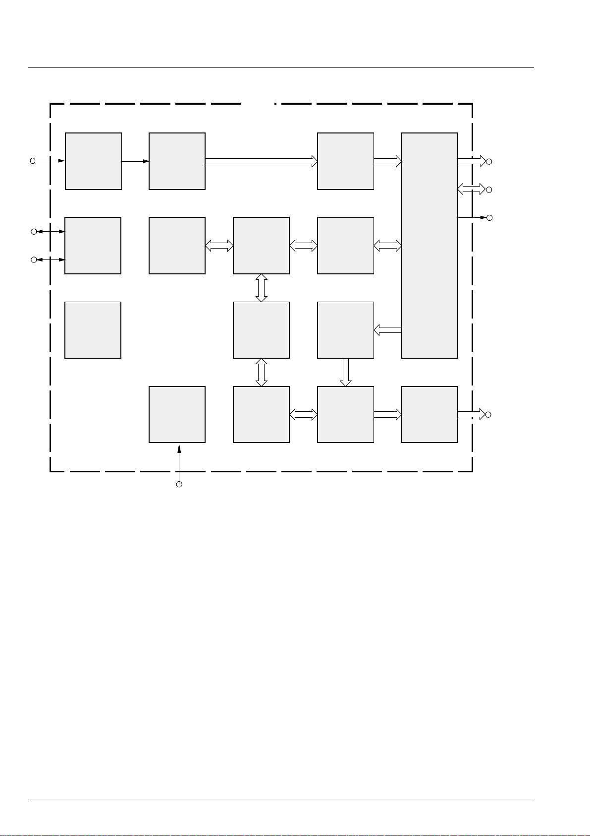
VCT 38xxA ADVANCE INFORMATION
TPU
Clamping
AGC
2
I
C Bus
Interface
Timer
Interrupt
Watchdog
ADC
Program
RAM
Sync
Interface
Program
ROM
DMA
Interface
Character
ROM
Slicer
65C02
WST
Layer
OSD
Layer
SRAM
Interface
Color &
Prio
Interface
Fig. 3–1: Block diagram of the TPU
48 Micronas
Page 49
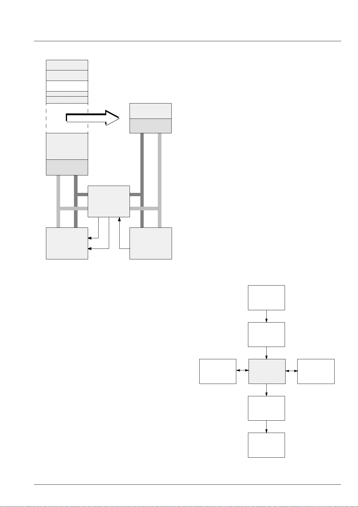
ADVANCE INFORMATION VCT 38xxA
3.5. Teletext Page Management
Zero Page
Stack Page
I/O Page
Extra Page
0000
1000
12K
Character ROM
8000
BE
RDY
D000
DMA
Interface
DATA
Display
BUSREQ
ADR
12K
Program ROM
ADR
DATA
65C02
Fig. 3–2: Memory environment of text controller
As a state-of-the-art teletext decoder, the TPU is able
to store and manage a sufficient number of teletext
pages to absorb the annoying transmission cycle
times. The number of available pages is only limited by
the memory size. With an intelligent software and a
4-Mbit SRAM it is possible to store and to control more
than 500 teletext pages.
The management of such a data base is a typical software task and is therefore performed by the 65C02.
Using a fixed length page table with one entry for every
possible page, the software distributes the content of
the acquisition scratch buffer among the page memory.
The page size is fixed to 1 kByte, only ghost rows are
chained in 128-Byte segments to avoid unused memory space.
A stored teletext page cannot be displayed directly,
because of the row-adaptive transmission and the
level 2 enhancements (row 26
−29). Therefore, the
CPU has to transfer the selected teletext page into a
display page buffer, adding extra data such as character set extension and non-spacing attributes.
3.5.1. Memory Manager
The Memory manager is the core of the internal TPU
firmware. Most of the acquisition and display related
functions are controlled by this management.
3.4. Teletext Acquisition
The only task of the slicer circuit is to extract teletext
lines from the incoming composite video signal and to
store them into the acquisition scratch buffer of the
internal/external SRAM. No page selection is done at
this hardware level.
Four analog sources can be connected, thus it is possible to receive text from one channel while watching
another on the screen. After clamping and AGC amplifier the analog video signal is converted into binary
data. Sync separation is done by a sync slicer and a
horizontal PLL, which generate the horizontal and vertical timing. By these means, no external sync signals
are needed and any available signal source can be
used for teletext reception.
The teletext information itself is acquired using adaptive slicers on bit and byte level with soft error detection to decrease the bit error rate under bad reception
conditions. The slicer can be programmed to different
bit rates for reception of PAL, NTSC or MAC world system teletext as well as VPS, WSS, or CAPTION signals.
Acquisition
Scratch
Memory
Page
Table
Memory
Manager
Display
Memory
Display
Controller
Fig. 3–3: Memory Manager
Page
Memory
Micronas 49
Page 50
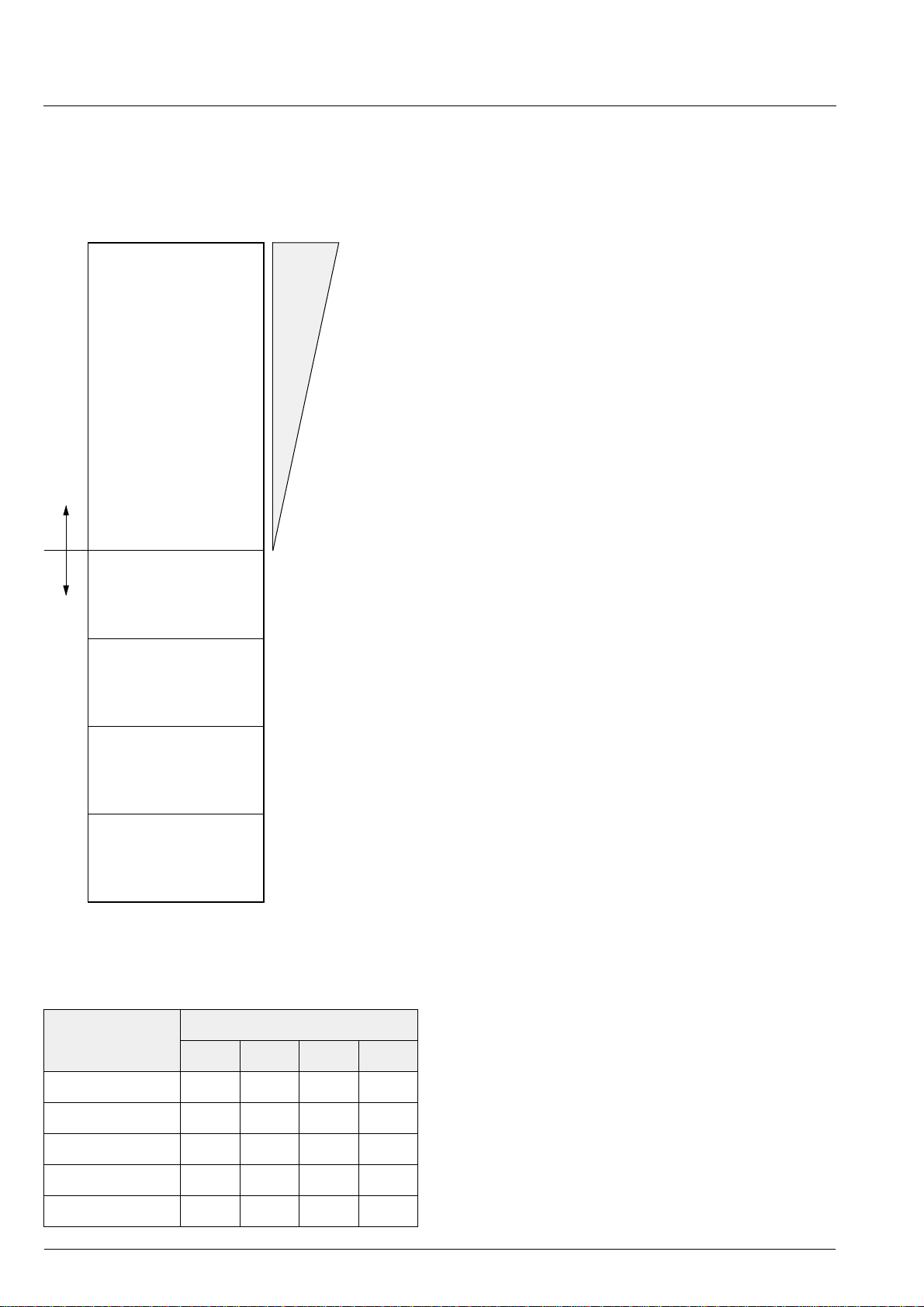
VCT 38xxA ADVANCE INFORMATION
08 00 00 = 4Mbit
02 00 00 = 1Mbit
00 80 00 = 256Kbit
00 40 00
00 30 00
00 20 00
00 10 00
00 00 00
4kBytes
TTX Display Bank
n x 1 kByte
Page Memory
SRAM
4kBytes
Display Bank
4kBytes
Page Table
4kBytes
Acquisition
Scratch
3.5.2. Memory Organization
The upper end of the memory is defined by the SRAM
size, the lower end can be defined with the
PAGE_MEMORY command. Default memory organization is shown in Fig. 3–4.
The memory organization depends on available SRAM
size. If external SRAM is not available, there is only
one display bank for OSD and teletext and the page
memory starts at a different location (see Table 3–1).
3.5.3. Page Table
The memory management is based on a fixed size
page table, which has entries for every hexadecimal
page number from 100 to 8FF. The page table starts
with page 800 and contains a 2-Byte page pointer for
every page.
The page table can be read with the command
READ_PAGE_INFO sending the page number and
reading the 2-Byte page pointer containing:
– SRAM pointer
– cycle flag
– memory flag
– subpage flag
– update flag
– protection flag
Fig. 3–4: Memory organization
Table 3–1: Memory Organisation
Memory
Segment
Address
Display Bank h’3000 h’4000 h’3000 h’0000
TTX Bank h’2000 h’4000 h’3000 h’0000
Page Table h’0000 h’0000 h’0000 no
Acquisition Scratch h’1000 h’1000 h’1000 no
SRAM Size
≥128k 19k 16k 3k
Page Memory h’4000 h’1800 h’1800 no
The SRAM pointer gives the location where the page
is stored in memory. The page size is fixed to 1 kByte,
only ghost rows are allocated dynamically.
The cycle flag will be set as soon as this page is
detected in the transmission cycle even if it cannot be
stored in memory. Only if the page is really stored in
memory, the memory flag will be set. The subpage flag
will be set for every page in cycle if the page subcode
is different from 0000H or 3F7FH. The update flag is
set every time a page is stored and will be reset only
for the display page after updating the display memory.
A page with protection flag set will never be removed
from memory.
The memory manager uses page priorities to decide
which pages should be stored or removed from memory. If no more memory is available, pages with lowest
priority are removed automatically and the higher priority pages are stored at their place. By setting the page
priority the programmer has control over the memory
management.
The page table is fully controlled by the memory manager and should never be written by external software.
To change the page table flags the command
CHANGE_PAGE_INFO can be used.
50 Micronas
Page 51
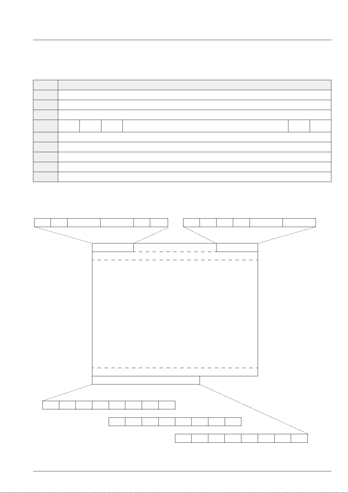
ADVANCE INFORMATION VCT 38xxA
Table 3–2: Page Table Format
Index 2-Byte Page Pointer
000
start magazine 8
001
...
100
Cycle
Flag
Memory
Flag
Subpage
Flag
11-bit SRAM Pointer Update
Flag
Protect
Flag
...
1F0
hexadecimal pages (e.g. TOP)
...
7FE
7FF
end magazine 7
status
language
subcode insubcode reqpriority
control
4−11
12−14
packet x/00
row flag
0−7
row flag
8−15
row flag
16−23
row flag
24−31
8 Byte8 Byte
ghost row pointer subpage pointer
packet x/01
1 kByte page data
packet x/24
24 Byte
subcode
high
subcode
low
indexpagemag
Fig. 3–5: Page format
Micronas 51
Page 52
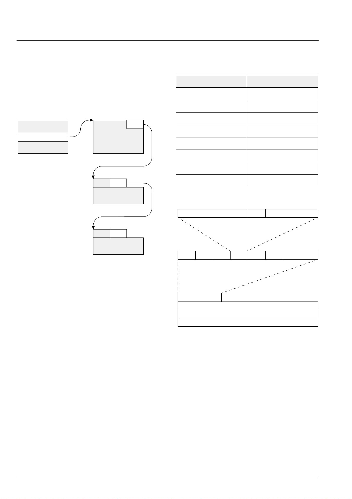
VCT 38xxA ADVANCE INFORMATION
ghost
pointer
Page Table
page 100
page pointer
ghost
pointer
ghost block
0000
ghost block
3.5.4. Ghost Row Organization
Page-related ghost rows are stored in blocks of
128 Bytes. These ghost blocks are linked together
using 2-Byte ghost row pointers. The first pointer can
be found in the basic page, all following pointers are
part of the block header. A zero pointer indicates the
end of the chain.
Table 3–3: Ghost Row Identification
Row Number Tag Row
000 empty
001 row 25
010 row 26
011 row 27
100 row 28
101 row 29
110 row 30
111 row 31
3-bit row number4-bit designation code
Fig. 3–6: Ghost row organization
Every ghost block contains 3 ghost rows which can be
identified by 3 row identification bytes in the block
header. The row identification contains designation
code and row number. The row number is reduced to a
3-bit tag. All ghost rows in one block belong to the
same page. If the memory manager removes a page
from memory, the linked ghost blocks will also be
removed.
3.5.5. Subpage Manager
Any page in cycle can have a number of subpages,
identified by subcode. In normal mode the subpage
manager will acquire only one subpage of every
requested page. This subpage can be any if subcode
FFFF is requested or it will be selected according to
the requested subcode.
After a PAGE_REQUEST command with subcode
F0xx, the subpage manager will acquire all subpages
of the requested page. The subpages will be chained
in the same order as they are transmitted, i.e. every
new subcode will be added at the end of chain. The
page table entry points to the subpage which was
transmitted first after the page request. The
‘aa’‘aa’‘aa’ row 2row 1 row 3 ghost row pointer
8 Byte block header
40 Byte row 1 data
40 Byte row 2 data
40 Byte row 3 data
Fig. 3–7: Ghost block structure
READ_PAGE_INFO command will reply the page
table pointer and the actual number of subpages in
chain.
After a PAGE_REQUEST command with subcode
F1xx, the subpage manager will acquire all subpages
of the requested page but will allocate only a limited
amount of memory to store these subpages. The
parameter “page subcode low” will define the length (in
number of subpages) of a ring buffer in page memory
which will hold the recently received subpages. In this
case, the READ_PAGE_INFO command will return an
index pointing to the most recently updated subpage in
chain, together with the subcode of this page.
52 Micronas
Page 53
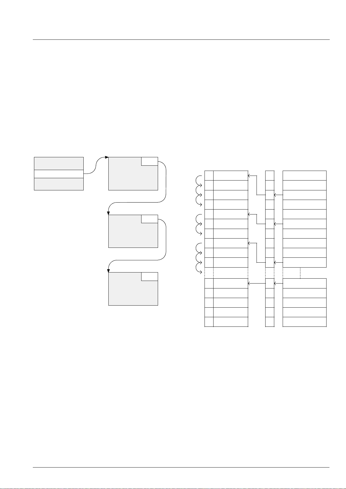
ADVANCE INFORMATION VCT 38xxA
The DISPLAY_PAGE_REQUEST command searches
and displays a page according to the requested display subcode. The search starts from page table and
continues through the subpage chain if there is any. A
rolling header will be displayed if the requested subpage cannot be found in memory.
A requested display subcode FFFF (don’t care subcode) will only search and display the first subpage in
chain, thus there is no rolling subpage anymore. A
DISPLAY_PAGE_REQUEST command with subcode
F0xx (follow subcode) will search and display the last
received subpage in chain, thus it is possible to
request all subpages in background while still showing
rolling subpages in display.
Page Table
page pointer
page 100
subcode 0003
page 100
subcode 0001
subpage
pointer
subpage
pointer
3.6. WST Display Controller
The display controller reads data from a display page
buffer in the internal/external SRAM. The display page
buffer is organized in rows which are separated into
level 1 data such as character codes and spacing
attributes and into level 2 data, such as character set
extension and non-spacing attributes. To limit the
memory amount for level 2 data, a slightly modified
stack model is used, in which one pointer bit for every
character location indicates the presence of additional
parallel attributes. Fig. 3–9 shows the organization of
the stack row buffer. In this stack model the number of
non-spacing attributes per row is limited to 40, which
agrees with the WST and CEPT specification.
Level 2 Buffer
Char 3 Attr.
1
Char 3 Attr.
1
Char 3 Attr.
1
0
Char 3 Attr.
1
Char 6Attr.
Char 6 Attr.
1
0
Char 6 Attr.
1
Char 10 Attr.
1
Char 10 Attr.
Char 10 Attr.
1
Pointer
0
0
1
0
0
1
0
0
0
1
Level 1 Buffer
Char 1
Char 2
Char 3
Char 4
Char 5
Char 6
Char 7
Char 8
Char 9
Char 10
Fig. 3–8: Subpage organization
page 100
subcode 0002
0000
0
Char 36 Attr.
0
0
0
0
1
0
0
0
0
Char 36
Char 37
Char 38
Char 39
Char 40
Fig. 3–9: Stack Row Buffer
The display controller includes two row buffers. The
first row buffer holds a copy of a teletext row from the
display page buffer. This decreases the data rate
through the SRAM interface by a factor of 10 or 8,
because new teletext row data is needed only after
10 lines in PAL or 8 lines in NTSC mode. The second
row buffer stores all display attributes in parallel, to
allow level 2 display without additional decoding.
Micronas 53
Page 54

VCT 38xxA ADVANCE INFORMATION
To present a WST level 2 display, the teletext display
controller has to evaluate the following attributes in
parallel, that is for every character location:
– 10-bit character code
– 5-bit foreground color
– 5-bit background color
– 2-bit size
– 5-bit flash
– 1-bit invert
– 1-bit separated
– 1-bit conceal
– 1-bit underline
– 1-bit boxing/window
Additional attributes are defined to improve the display
of CAPTION and OSD text:
– 1-bit italics
– 1-bit shadow
– 1-bit color mode
The display controller delivers 5-bit digital color information, a shadow signal for contrast reduction, and a
fast blank signal. The color bus is used to address the
color-lookup-table (CLUT) in the video processor. By
this means, the full level 2 color spectrum can be displayed.
54 Micronas
Page 55
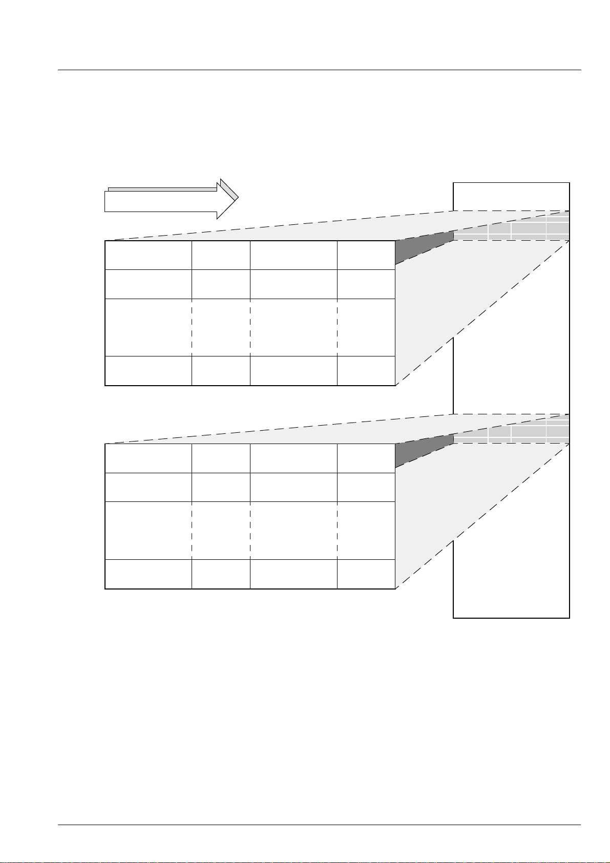
ADVANCE INFORMATION VCT 38xxA
3.7. Display Memory
The TPU supports a variable number of display memories, each 4 kBytes large. One bank is used to store
the display information of the selected teletext page.
The bank location can be defined with the command
autoincrement
Row 0
Row 1
40 Byte level 1 40 Byte level 2 full row attr.40-bit pointer
40 Byte level 1 40 Byte level 2 full row attr.40-bit pointer
Display Bank
Row 46
40 Byte level 1 40 Byte level 2 full row attr.40-bit pointer
DISPLAY_TTX_POINTER. Other banks can be used
to store any kind of display data in level 1 or level 2 format. Switching between these banks is fast and can be
programmed with the command DISPLAY_POINTER.
Bank switching allows generation of OSD menus without affecting the teletext display.
Row 0
Row 1
40 Byte level 1 40 Byte level 2 full row attr.40-bit pointer
40 Byte level 1 40 Byte level 2 full row attr.40-bit pointer
TTX Display Bank
Row 25
40 Byte level 1 40 Byte level 2 full row attr.40-bit pointer
Fig. 3–10: Display memory organization (level 2)
SRAM
Micronas 55
Page 56
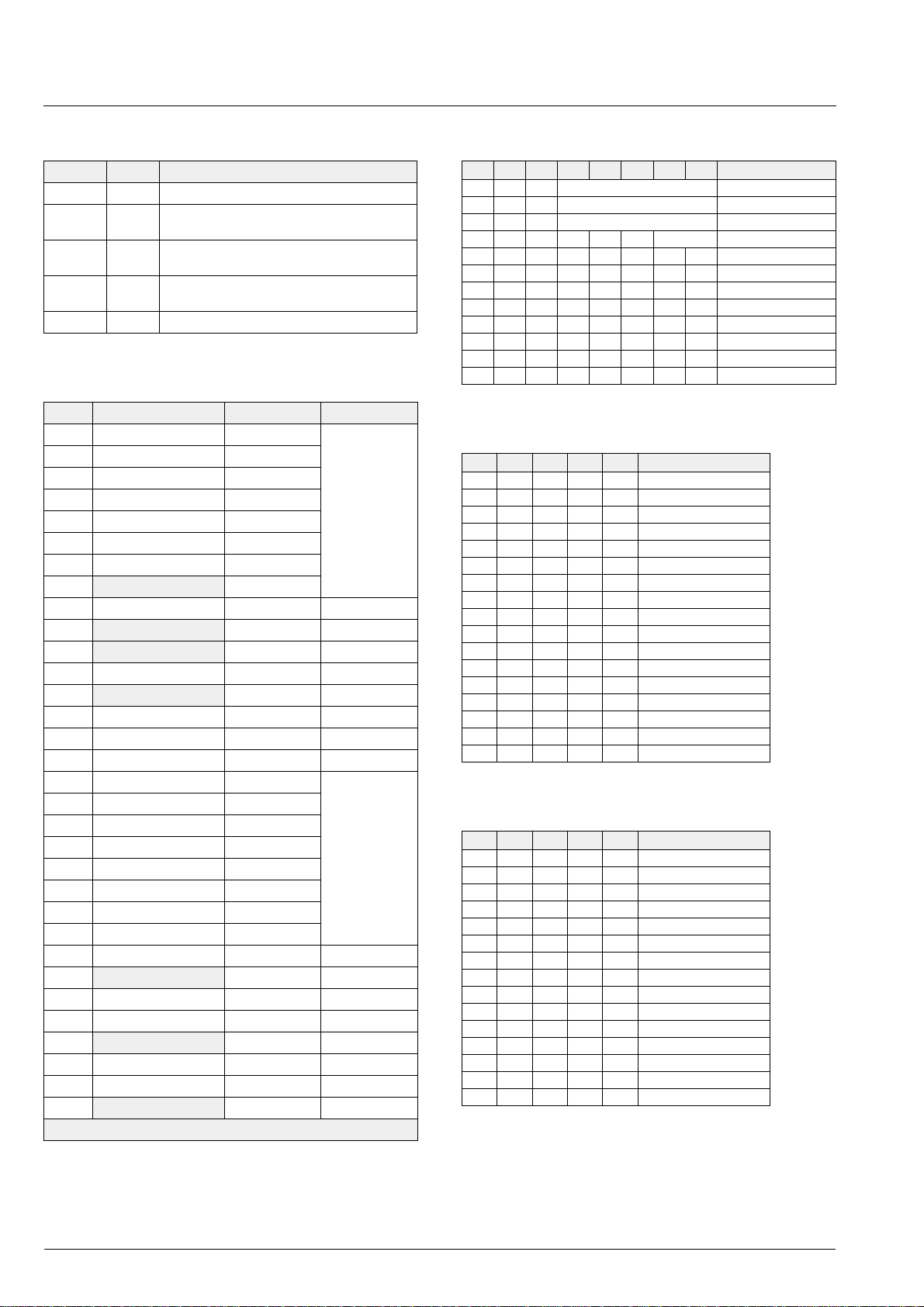
VCT 38xxA ADVANCE INFORMATION
Table 3–5: Full row attribute
+ 55H R/W Full Row Attribute
Bit Reset Function
7 - 1 = row is displayed blank
0 = row is displayed using row data
6 - 1 = row is displayed in double height
0 = row is displayed in normal height
5 - 1 = row is displayed in level 2 mode
0 = row is displayed in level 1 mode
4 to 0 - 5-bit value defining full row background color
Table 3–6: Level 1 spacing attributes
Code Function Action Notes
00 Alpha Black set alpha
01 Alpha Red
02 Alpha Green
03 Alpha Yellow
04 Alpha Blue
05 Alpha Magenta
06 Alpha Cyan
07
Alpha White
08 Flash Normal
09
Flash Off set at
0A
Boxing Off set at double
0B Boxing On set at double
0C
Size Normal set at
0D Size Double Height
0E Size Double Width
0F Size Double
10 Mosaic Black set mosaic
11 Mosaic Red
12 Mosaic Green
13 Mosaic Yellow
14 Mosaic Blue
15 Mosaic Magenta
16 Mosaic Cyan
17 Mosaic White
18 Conceal set at
19
Contiguous Mosaic set at
1A Separated Mosaic set at
1B ESC
1C
Black Background set at
1D New Background set at
1E Hold Mosaic set at
1F
Release Mosaic
Shaded attributes are default at start of each display row.
mode and
foreground
color of
following alpha
characters
select
character set 0
mode and
foreground
color of
following
mosaic
characters
select
character set 1
Table 3–7: Level 2 parallel attributes
7 6 5 4 3 2 1 0 Function
P 0 0 Color Foreground Color
P 0 1 Color Background Color
P 1 0 Flash Flash Mode
P1100L Set Character Set
P11010DHDWSize
P110110UUnderline/Separated
P110111I Inverted
P111000CConceal
P111001WWindow/Boxing
P111010SShadow
P111011ITItalic
P111100CMColor Mode
Table 3–8: Color look-up table
4 3 2 1 0 Display Color
00000Black
00001Red
00010Green
00011Yellow
00100Blue
00101Magenta
00110Cyan
00111White
0 1 0 0 0 Transparent
01001Reduced Red
01010Reduced Green
01011Reduced Yellow
01100Reduced Blue
01101Reduced Magenta
0 1 1 1 0 Reduced Cyan
01111Reduced White
1 x x x x Programmable
Table 3–4: Flash modes
4 3 2 1 0 Function
00000Off
00001Normal
00101Normal Fast Phase 1
01001Normal Fast Phase 2
01101Normal Fast Phase 3
00010Inverted
00110Inverted Fast Phase 1
01010Inverted Fast Phase 2
01110Inverted Fast Phase 3
00011Color Table
00111Color Table Phase 1
01011Color Table Phase 2
01111Color Table Phase 3
1 0 0 x x Incremental
1 0 1 x x Decremental
56 Micronas
Page 57
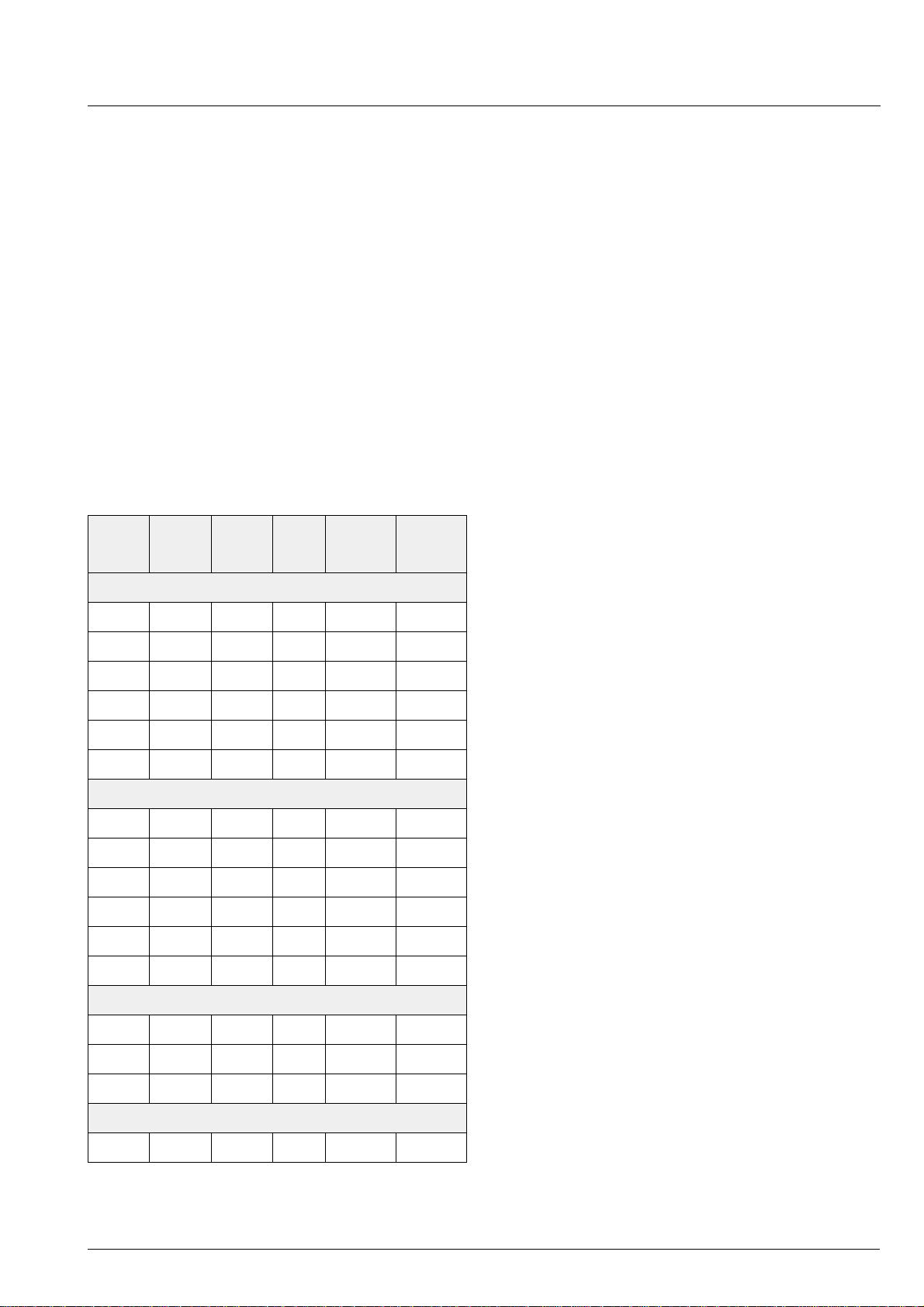
ADVANCE INFORMATION VCT 38xxA
3.8. Character Generator
Characters are addressed using a 10-bit character
code. The 2 MSBs of the character code define 1 of 4
character sets. Character set selection is done using
level 2 parallel attributes (see Table 3–7 on page 56).
Each character set contains 224 characters. The first
32 characters in each character set are reserved for
control codes (see Table 3–6 on page 56). On a single
screen, 896 different characters can be displayed.
Characters can be displayed in several pixel resolutions provided that the according font is available. The
character generator supports horizontal resolution of
8 or 10 pixel/char and vertical resolution of 8, 10, or
13 lines/char. Characters can be combined without
separating borders to create more complex character
definitions (e.g. kanji or icons).
Table 3–9: Character resolutions
matrix
(h x v)
10 x 8 40 x 32 40 x 28 40
8 x 10 40 x 26 40 x 22 32
10 x 10 40 x 26 40 x 22 40
8 x 13 40 x 20 40 x 17 32
10 x 13 40 x 20 40 x 17 40
16 x 16 20 x 16 20 x 14 32
20 x 16 20 x 16 20 x 14 40
16 x 20 20 x 13 20 x 11 32
20 x 20 20 x 13 20 x 11 40
16 x 26 20 x 10 20 x 8.5 32
20 x 26 20 x 10 20 x 8.5 40
16 x 10 20 x 26 20 x 22 32
char/sc
reen
(PAL)
8 x 8 40 x 32 40 x 28 32
char/sc
reen
(NTSC)
single character
combined character (2 x 2)
combined character (2 x 1)
osd
width
# char in
12k font
µs 1600 2560
µs 1280 2048
µs 1280 2048
µs 1024 1638
µs 800 1280
µs 640 1024
µs 400 640
µs 320 512
µs 320 512
µs 256 409
µs 200 320
µs 160 256
µs 640 1024
# char in
20k font
The pixel clock can be either 10.125 MHz or
20.25 MHz. To get 10-bit pixel information from the
character font, two memory cycles are needed. The
character font is part of the mask-programmable ROM,
but supplied with its own bus structure (see Fig. 3–2 on
page 49). By this means the data transfer between
character ROM and teletext display controller does not
stop the CPU.
Both bus structures are connected via a memory interface which allows cross-connections using DMA or
wait cycles. If the character font size exceeds
12 kBytes, part of the character font can be shifted into
the program ROM which causes DMA cycles. Therefore only less frequently used characters should be
placed into the program ROM. Vice versa seldom used
CPU code can be put into the character ROM.
The WST specification defines a number of 7-bit code
tables, which are filled with 96 characters only (the
MSB is used for parity check). In the G0 code table
some characters have several language dependent
variations. Additionally characters from the G0 code
table can be combined with diacritical marks from the
G2 code table (row 26). Furthermore different code
tables are defined for languages like cyrillic, greek or
arabic. Thus it is not possible to simply transform the
code tables into a continuous character font ROM without getting unused ROM space and multiple defined
character fonts.
This problem is solved by implementing a character
code mapping (see Fig. 3–11 on page 58). The
5 MSBs of each character code are mapped into
another 5-bit code which is then used to address the
character font ROM. By this means the whole character font is subdivided into 32 blocks of 32 characters
which can freely be distributed over the 4 character
sets.
The character code mapping is implemented as RAM
and can be programmed by software. After reset the
TPU initializes the mapping RAM for standard WST
latin code tables.
The TV controller can select predefined mappings for
latin, cyrillic and arabic teletext via the command
DISPLAY_MODE (see Table 3–16 on page 70). The
same command allows selection of a user defined
mapping which has to programmed in advance using
command USER_MAPPING.
16 x 13 20 x 20 20 x 17 32
20 x 13 20 x 20 20 x 17 40
combined character (1x 2)
10 x 16 40 x 16 40 x 14 40
µs 400 640
µs 320 512
µs 640 1024
Micronas 57
Page 58
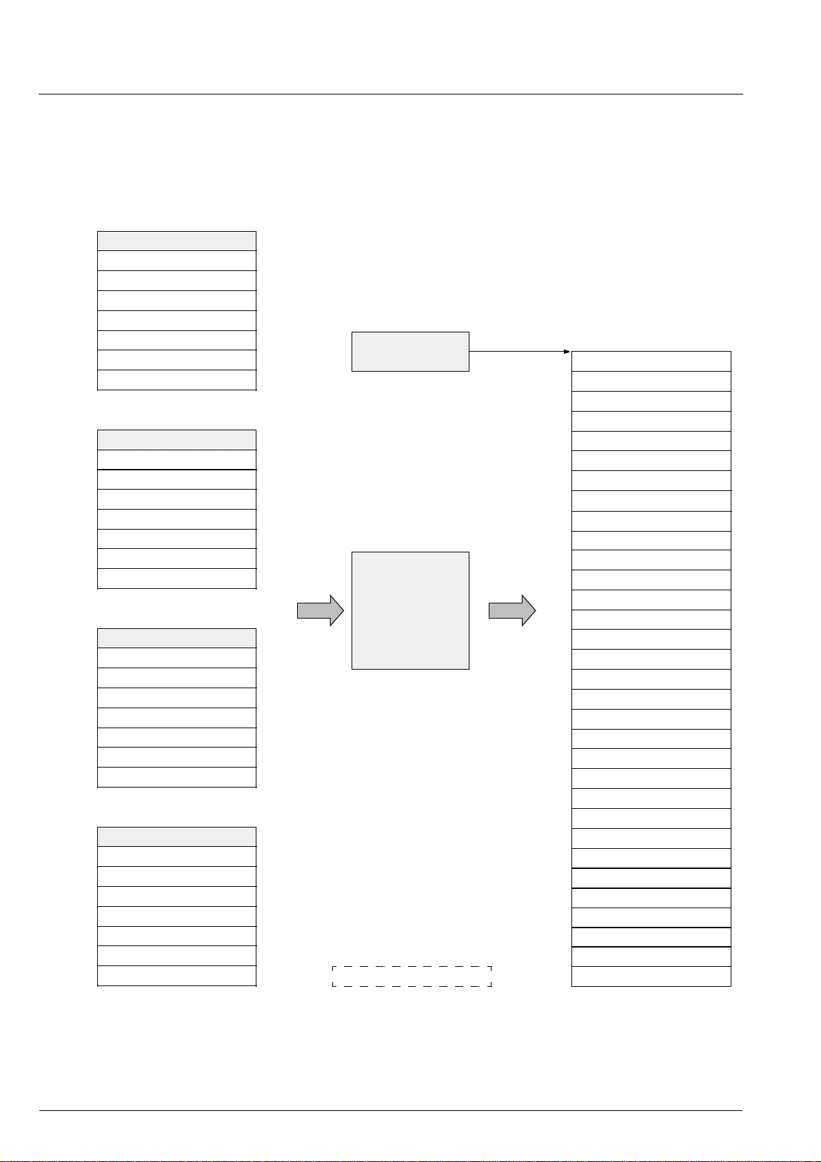
VCT 38xxA ADVANCE INFORMATION
3.8.1. Character Code Mapping
10-bit Character Code = 2-bit Character Set (level 2) + 8-bit Character Value (level 1)
Character Set 0
000H
080H
100H
180H
200H
280H
300H
380H
G0
G0
G0
National
National
National
National
Character Set 1
G1
G0
G1
National
National
National
National
Character Set 2
G2
G2
G2
User
User
User
User
Character Set 3
G3
G3
G3
User
User
User
User
00
01
02
03
04
05
06
07
08
09
10
11
12
13
14
15
16
17
18
19
20
21
22
23
24
25
26
27
28
29
30
31
Font Pointer
Mapping RAM
32 x 5 bit
block of 32 char
00
01
02
03
04
05
06
07
08
09
10
11
12
13
14
15
16
17
18
19
20
21
22
23
24
25
26
27
28
29
30
31
Character ROM
12800 Byte
G0
G0
G0
National
National
National
National
G1
G1
G2
G2
G2
User
User
User
User
G3
G3
G3
Greek
Greek
Cyrillic
Cyrillic
Cyrillic
Hebrew
Arabic
Arabic
Arabic
Farsi
Fig. 3–11: Character code mapping
58 Micronas
Page 59
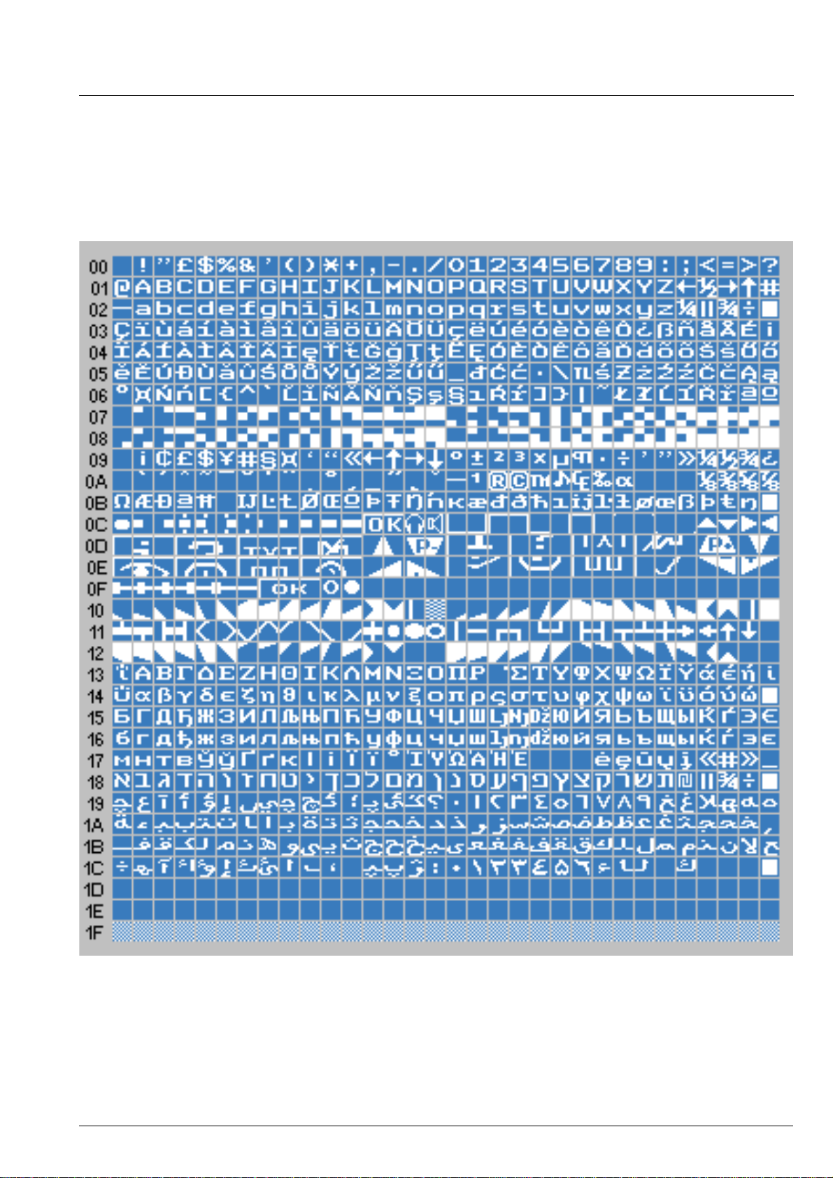
ADVANCE INFORMATION VCT 38xxA
3.8.2. Character Font ROM
The character font ROM is mask-programmable.
Design of customer specific characters (user font) is
supported by a Windows™ based PC tool named
MOFA (Micronas OSD and Font Assembler). In combi-
nation with the VCT 38xxA emulator board it is possible to download character fonts and verify them on the
TV screen.
Fig. 3–12: Character font ROM
Micronas 59
Page 60
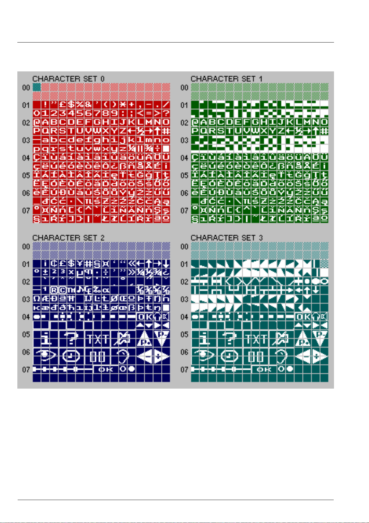
VCT 38xxA ADVANCE INFORMATION
3.8.3. Latin Font Mapping
Fig. 3–13: Latin font mapping
60 Micronas
Page 61
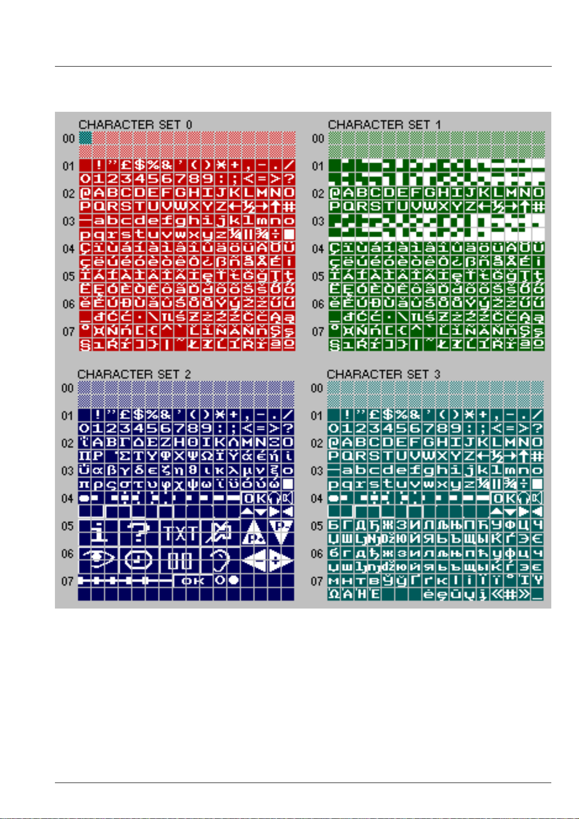
ADVANCE INFORMATION VCT 38xxA
3.8.4. Cyrillic Font Mapping
Fig. 3–14: Cyrillic font mapping
Micronas 61
Page 62
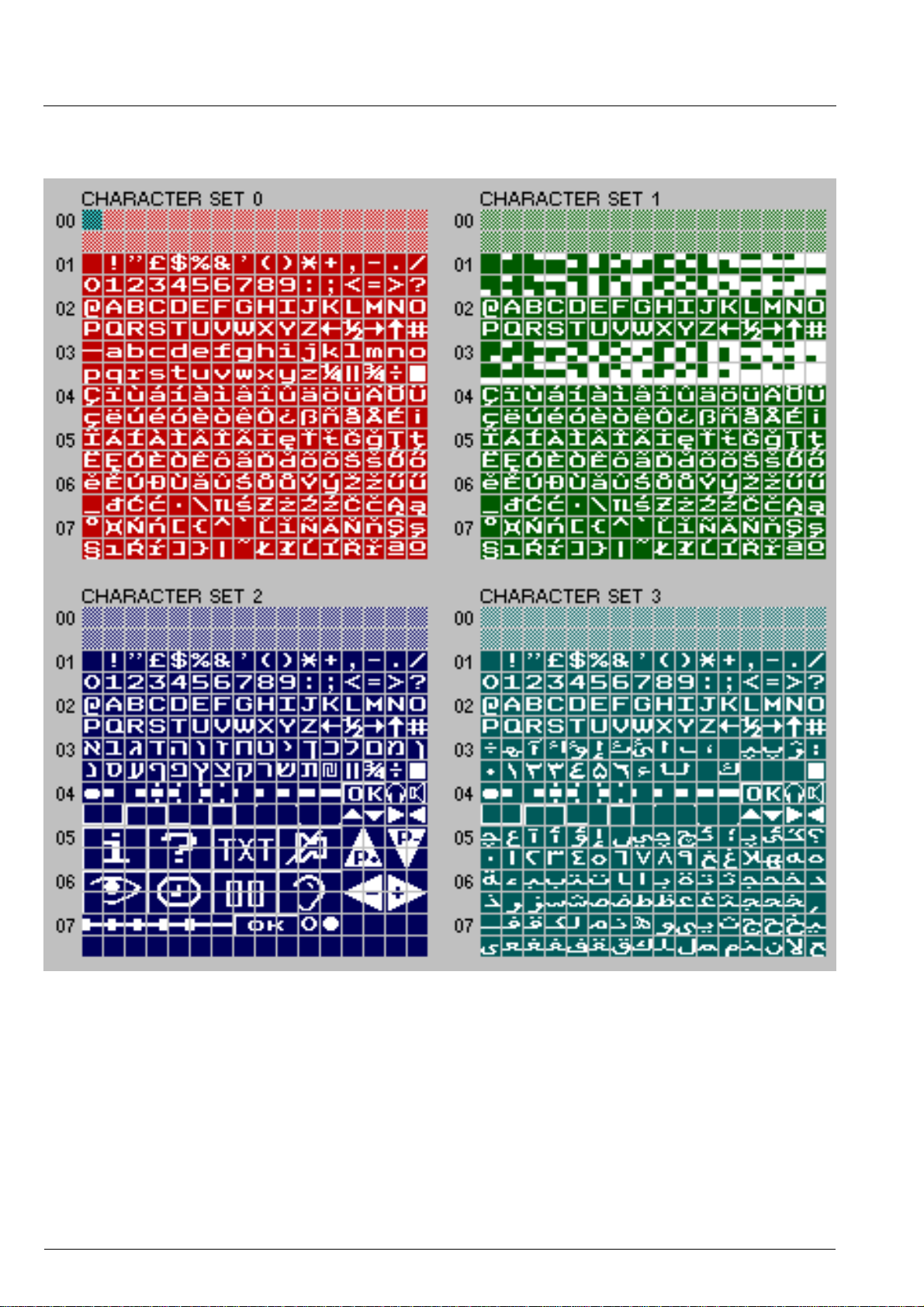
VCT 38xxA ADVANCE INFORMATION
3.8.5. Arabic Font Mapping
Fig. 3–15: Arabic font mapping
62 Micronas
Page 63
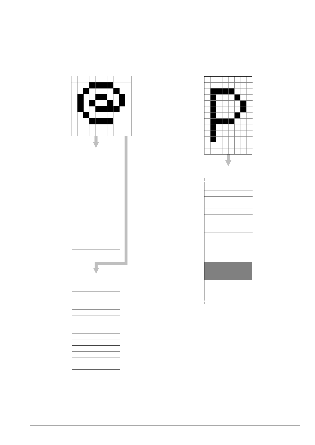
ADVANCE INFORMATION VCT 38xxA
3.8.6. Character Font Structure
Line 1
Line 2
Line 3
Line 4
Line 5
Line 6
Line 7
Line 8
Line 9
Line 10
Line 1
Line 2
Line 3
Line 4
Line 5
Line 6
Line 7
Line 8
Line 9
Line 10
Line 1
Line 2
Line 3
Line 4
Line 1
Line 2
Line 3
Line 4
Line 5
Line 6
Line 7
Line 8
Line 9
Line 10
Line 1
Line 2
Line 3
Line 4
Character Font
‘@‘
‘@‘
‘@‘
‘@‘
‘@‘
‘@‘
‘@‘
‘@‘
‘@‘
‘@‘
‘A‘
‘A‘
‘A‘
‘A‘
Extension Font
‘@‘
‘A‘
‘B‘
‘@‘
‘A‘
‘B‘
‘@‘
‘A‘
‘B‘
‘@‘
‘A‘
‘B‘
‘@‘
‘A‘
‘B‘
‘@‘
‘A‘
‘B‘
‘@‘
‘A‘
‘B‘
‘@‘
‘A‘
‘B‘
‘@‘
‘@‘
‘D‘
‘D‘
‘D‘
‘D‘
‘A‘
‘A‘
‘E‘
‘E‘
‘E‘
‘E‘
‘B‘
‘B‘
‘F‘
‘F‘
‘F‘
‘F‘
‘C‘
‘C‘
‘C‘
‘C‘
‘C‘
‘C‘
‘C‘
‘C‘
‘C‘
‘C‘
‘G‘
‘G‘
‘G‘
‘G‘
LSBMSB
09
MSB
7
Line 1
Line 2
Line 3
Line 4
Line 5
Line 6
Line 7
Line 8
Line 9
Line 10
Line 11
Line 12
Line 13
LSB
0
Character Font
Line 1
Line 2
Line 3
Line 4
Line 5
Line 6
Line 7
Line 8
Line 9
Line 10
Line 11
Line 12
Line 13
Line 14
Line 15
Line 16
Line 1
Line 2
Line 3
Fig. 3–17: Font structure 8 x 13
‘P‘
‘P‘
‘P‘
‘P‘
‘P‘
‘P‘
‘P‘
‘P‘
‘P‘
‘P‘
‘P‘
‘P‘
‘P‘
‘Q‘
‘Q‘
‘Q‘
Fig. 3–16: Font Structure 10 x 10
Micronas 63
Page 64
VCT 38xxA ADVANCE INFORMATION
3.9. National Character Mapping
Table 3–10: Character set options
Option Bits
C14,C13,C12
000 English Polish English (US) English English (US) programmable
001 French French French French Slovakian programmable
010 Swedish Swedish Swedish Swedish Hungarian programmable
011 Czech Czech Czech Turkish Serbian programmable
100 German German German German Albanian programmable
101 Spanish Serbian Spanish Spanish Polish programmable
110 Italian Italian Italian Italian Turkish programmable
111 Estonian Estonian Estonian Estonian Rumanian programmable
6 38 40 55 70 128
Table 3–11: Language codes
Code Language
0
1
2
3
4
5
6
7
8
9
10
11
12
13
14
15
16
17
18
19
20
21
22
23
24
25−255
English
French
Swedish, Finnish
Czech
German
Spanish
Italian
Estonian, Finnish
English (US)
Slovakian
Hungarian
Serbian, Croatian, Slovene
Albanian
Polish
Tu r k i sh
Rumanian
Cyrillic (Russian, Bulgarian)
Greek
Cyrillic (Serbian, Montenegro)
YU Latin
Arabic
Hebrew
Farsi
Lettish, Lithuanian
Cyrillic (Ukrainian)
not defined
Character Set
64 Micronas
Page 65

ADVANCE INFORMATION VCT 38xxA
Table 3–12: National option mapping
Language
2/3 2/4 4/0 5/11 5/12 5/13 5/14 5/15 6/0 7/11 7/12 7/13 7/14
Albanian 5/15 2/4 13/12 13/2 12/12 12/3 11/12 9/1 13/13 13/3 12/13 13/1 11/13
Czech 5/15 12/9 13/13 10/11 12/13 12/11 8/4 15/13 9/3 8/3 12/0 9/2 11/13
English 2/3 2/4 4/0 5/11 5/12 5/13 5/14 5/15 6/0 7/11 7/12 7/13 7/14
English (US) 5/15 2/4 4/0 14/4 13/5 15/4 14/6 13/0 14/7 14/5 15/6 15/5 15/7
Estonian, Finnish 5/15 11/11 11/12 8/13 8/14 12/12 8/15 11/10 11/13 8/10 8/11 12/13 8/12
French 9/3 8/1 8/5 9/1 9/7 8/2 8/8 5/15 9/5 8/7 9/8 8/9 9/0
German 5/15 2/4 15/0 8/13 8/14 8/15 14/6 13/0 14/0 8/10 8/11 8/12 9/10
Hungarian 5/15 9/2 9/14 8/4 8/14 10/1 12/15 11/15 9/3 9/4 8/11 8/3 8/12
Italian 2/3 2/4 9/3 14/0 9/0 5/13 5/14 5/15 8/2 8/5 9/6 9/5 8/6
Polish 5/15 14/3 13/15 13/8 12/7 15/8 13/3 9/4 10/9 13/9 13/7 15/9 13/11
Rumanian 5/15 14/1 10/14 10/5 14/14 14/11 10/6 15/1 10/15 8/7 14/15 12/5 8/8
Serbian, Croatian 5/15 2/4 13/12 13/2 12/12 12/3 11/12 13/0 13/13 13/3 12/13 13/1 11/13
Slovakian 5/15 12/9 13/13 10/11 12/13 12/11 8/4 15/13 9/3 8/3 12/0 9/2 11/13
Spanish 9/0 2/4 9/15 8/3 9/3 8/4 9/4 9/2 9/9 8/12 9/11 9/5 8/5
G0/G1 Table Position
Swedish, Finnish 5/15 14/1 9/14 8/13 8/14 9/13 8/15 13/0 9/3 8/10 8/11 9/12 8/12
Turkish 13/6 10/13 10/8 14/14 8/14 8/0 8/15 10/12 15/1 14/15 8/11 9/0 8/12
YU Latin 5/15 2/4 13/12 13/2 12/12 12/3 11/12 13/0 13/13 13/3 12/13 13/1 11/13
Micronas 65
Page 66
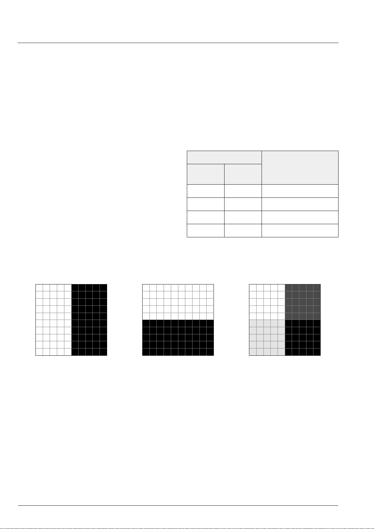
VCT 38xxA ADVANCE INFORMATION
3.10.Four-Color Mode
In “Four-Color Mode” the color depth of single or multiple characters can be increased to 4 colors (e.g. to display icons or 3-D effects). A special font organization is
required because two consecutive characters will be
combined. The number of 4-colored characters is only
limited by font size.
The “Four-Color Mode” is controlled via the level 2 parallel attribute “Color Mode”. Setting the bit CM to 1
activates the “Four-Color Mode” until the end of row or
until the bit CM is set to 0 again. At the start of each
display row the “Four-Color Mode” is disabled.
A character with active “Four-Color Mode” attribute will
be combined with its font neighbor to define a 2
bit/pixel character matrix. The 2 additional colors are
derived from the active foreground and background
colors by inverting bit 3 of the color code. Using the
programmable part of the CLUT it is possible to display
characters in 4 out of 4096 colors.
If the “Four-Color Mode” attribute is set for a character
with even character code n, this character is combined
with its font neighbor addressed by code n + 1. If the
“Four-Color Mode” attribute is set for a character with
odd character code, this character is combined with
itself.
The neighbor character does not change the definition
of foreground and background pixel which is used to
control flash and mix mode.
Table 3–13: Color Allocation
Pixel Definition Color Allocation
Character nCharacter
n+1
0 0 background
1 0 foreground
0 1 background .xor. 8
1 1 foreground .xor. 8
Matrix of Character n
Fig. 3–18: Four-color mode
+
Matrix of Character n+1 4 Color Display
00 10
=
01 11
66 Micronas
Page 67

ADVANCE INFORMATION VCT 38xxA
3.11.OSD Layer
Apart from the WST layer, there is an additional OSD
layer on chip. The OSD layer accesses the CPU memory via DMA to read text, display attributes, and character font information. The color outputs of the OSD
layer can have higher priority than the WST layer outputs. Thus, it is possible to overlay the teletext display
with an additional layer for user guidance (see Fig. 3–
19).
Full Screen Layer
WST Layer
OSD Layer
Fig. 3–19: Display layer
The OSD layer reads text strings addressed by a programmable text pointer. Codes smaller than 80h will
address the character font, codes greater or equal 80h
are interpreted as control codes to change color or
character set (see Table 3–14). After reading a control
code the OSD layer will do an additional read to get the
next character code.
Code Function Notes
01 Underline On only for 13 scanlines/character
02
03 Flash On
04
05 Italics On
06
07 Transparent layer becomes transparent
08 Shadow layer becomes transparent and
0C END end of layer
0D CR end of text line
0E
80
Shaded attributes are default at start of each text line.
Underline Off
Flash Off
Italics Off
contrast is reduced to 66%
− 7F ASCII Character using font 1 or font 2
− FF Control Code Only one control code per character
is allowed. Depending on OSD
Mode, the control code defines
either color or character set.
Color bit 0 = foreground color blue
bit 1 = foreground color green
bit 2 = foreground color red
bit 3 = background color blue
bit 4 = background color green
bit 5 = background color red
bit 6 = replace white by transparent
bit 7 = 1
Character Set bit 0 = bit 7 of character code
bit 1 = bit 8 of character code
bit 2 = bit 9 of character code
bit 3 =
bit 4 =
bit 5 =
bit 6 = latching shift to character set
bit 7 = 1
Micronas 67
Page 68

VCT 38xxA ADVANCE INFORMATION
3.12.Command Language
The TPU supports a command language, allowing the
TV controller to start complex processing inside the
TPU with simple commands. The TV controller is not
The application software has to send commands to the
TPU via I
2
C bus using the command subaddresse
SUB4 (see Section 3.14.1.3. on page 83).
burdened with time consuming tasks like page searching or data shuffling.
Tabl e 3 –15 lists all available commands. For a more
detailed description of the command language see
Tabl e 3 –16.
Table 3–15: Command language cross reference
Code Dec. Code Hex. Command Name No. Write
Parameter
0 00 Dummy 0 0 x000 0000
1 01 Reset 0 0 x000 0000
2 02 Escape 0 0 x000 0000
3 03 Version 0 2 x000 0000
4 04 Test 0 0 x000 0000
5 05 Test 0 0 x000 0000
6 06 DRAM Mode 3 0 x000 0000
7 07 Acquisition Mode 5 2 x000 0000
8 08 Display Mode 4 0 x000 0000
9 09 Display TTX Pointer 2 0 x000 0000
10 0a Display Pointer 3 0 x000 0000
11 0b Display Clear 2 0 x000 0000
12 0c Page Request 8 3 x0x0 0000
13 0d Display Time Pointer 2 0 x000 0000
14 0e Read DRAM Size 0 3 x000 0000
15 0f Read VPS 0 15 x0x0 0000
16 10 Read Quality 0 4 x000 0000
17 11 Read Display Mode 0 4 x000 0000
18 12 Read Reset Source 0 1 x000 0000
19 13 Read Rolling Header 0 24 x000 0000
20 14 Read Page Info 2 7 x000 0000
21 15 Read Page Row 5 40 x0x0 0000
22 16 Change Page Info 3 0 x000 0000
23 17 Search MPET 0 1 + (n*4) x0x0 0000
24 18 Read Display Page 0 4 x000 0000
25 19 Page Memory 2 0 x000 0000
26 1a Display Page Request 5 0 x000 0000
27 1b Page Table Reset 0 0 x000 0000
28 1c Search Next Page 3 6 x0x0 0000
29 1d Read Page Cycle 0 9 x000 0000
30 1e Read TOP Code 2 2 x000 0000
31 1f Read Rolling Time 0 8 x000 0000
32 20 Copy Page Row 8 0 x0x0 0000
33 21 Copy Data 7 0 x000 0000
34 22 Search Next TOP Code 3 4 x0x0 0000
35 23 Read Ghost Row 6 40 x0x0 0000
No. Read
Parameter
Status Register
68 Micronas
Page 69

ADVANCE INFORMATION VCT 38xxA
Table 3–15: Command language cross reference
Code Dec. Code Hex. Command Name No. Write
Parameter
36 24 Read 8/30 Row 1 40 x0x0 0000
37 25 Read Priority 0 5 x000 0000
38 26 Page Priority 2 0 x000 0000
39 27 Search AIT 0 1 + (n*4) x0x0 0000
40 28 Read TOP Status 0 2 x000 0000
41 29 Search AIT Title 2 17 x0x0 0000
42 2a Reset Ghost Row Status 0 0 x000 0000
43 2b Search MPT 0 1 + (n*4) x0x0 0000
44 2c Copy AIT Title 5 17 x0x0 0000
45 2d Search Direct Choice 1 1 + (n*2) x0x0 0000
46 2e Read Hamming 1 1 x000 0000
47 2f Read Hamming 2 3 3 x000 0000
48 30 Display Column 3+length 0 x000 0000
49 31 Display Fill 4 0 x000 0000
50 32 Read BTTL 0 9 x0x0 0000
51 33 Read Next Page 2 2 x000 0000
52 34 Change BTT magazine 1 0 x000 0000
53 35 Read WSS 0 15 x0x0 0000
54 36 Read CAPTION 1 0 7 x0x0 0000
55 37 Read CAPTION 2 0 7 x0x0 0000
56 38 OSD Font Pointer 5 0 x000 0000
57 39 Display Read Column 3 length x000 0000
58 3a User Character Set 8 0 x000 0000
59 3b User ESC Character Set 8 0 x000 0000
60 3c Full Row Attribute 3 0 x000 0000
61 3d User Mapping 32 0 x000 0000
No. Read
Parameter
Status Register
Micronas 69
Page 70

VCT 38xxA ADVANCE INFORMATION
Note:
If not otherwise designated, all parameters in the following table are specified as single bytes. As write
parameter magazine numbers 8 and 0 have the same meaning, as read parameter the magazine number is a
true 4-bit number (e.g. magazine 8= 00001000). For write parameters the values in parentheses indicate
default values after reset (in hex notation). For compatibility reasons every undefined bit in a write parameter should be set to ‘0’. Undefined bits in a read parameter should be treated as “don’t care”.
Table 3–16: Command language
Code Function Write Parameter Read Parameter Notes
Operational & Test Commands
00 Dummy no action
01 Reset software reset of 65C02
02 Escape escape to other codes
03 Version CPU pointer high
04 Test reserved for testing
05 Test reserved for testing
06 DRAM Mode dram mode (06)
flash inc (05)
control enable (FF)
07 Acquisition Mode acquisition mode (00)
init subcode high (FF)
init subcode low (FF)
gain max (1F)
filter max (1F)
Memory Management Commands
14 Read DRAM Size dram size high
25 Page Memory dram bank (00)
dram high (40)
27 Page Table Reset reset page table
CPU pointer low
gain
filter
dram size low
dram mode
show version in OSD layer
CPU pointer to text in ROM
dram mode = I/O page register 028EH
flash freq = flash inc / (256 * 0.00324)
control enable:
bit0 = C4 erase page
bit1 = C5 news flash
bit2 = C6 subtitle
bit3 = C7 suppress header
bit4 = C8 update indicator
bit5 = C9 interrupted sequence
bit6 = C10 inhibit display
bit7 = C11
acquisition mode:
bit0 = no slicer adaption
bit1 = no bit error in framing code
bit2 = limit slicer adaption
init subcode:
automatic subcode request after
page table reset
gain max: only used if bit2 = 1
filter max: only used if bit2 = 1
dram size:
000CH = 3kByte SRAM
004CH = 19kByte SRAM
0200H = 128kByte SRAM
0240H = 144kByte SRAM
0400H = 256kByte SRAM
0800H = 512kByte SRAM
dram mode:
see I/O page register 028EH
start of page memory
execute page table reset
reset ghost row status
reset data service status
reset cycle count
reset memory count
reset ghost count
reset priorities
clear rolling header
clear VPS data
clear WSS data
magazine parallel
70 Micronas
Page 71

ADVANCE INFORMATION VCT 38xxA
Table 3–16: Command language, continued
Code Function Write Parameter Read Parameter Notes
42 Reset Ghost Row Status ghost row status:
29 Read Page Cycle ghost row status
38 Page Priority enable (00)
border (FF)
37 Read Priority highest priority
Page Related Commands
12 Page Request magazine number
page number
page subcode high
page subcode low
priority
quantity
start magazine number
start page number
20 Read Page Info magazine number
page number
22 Change Page Info magazine number
page number
page table flags
2 Byte cycle count
2 Byte memory count
2 Byte ghost count
data service status
memory status
lowest priority
border priority
magazine number
page number
number of open requests
removed magazine
number
removed page number
page pointer high
page pointer low
subpage count
ghost row count
ring buffer index
page subcode high
page subcode low
bit0 = row 24 in cycle
bit1 = row 25 in cycle
bit2 = row 26 in cycle
bit3 = row 27 in cycle
bit4 = row 28 in cycle
bit5 = row 29 in cycle
bit6 = row 30 in cycle
bit7 = row 31 in cycle
= number of pages in cycle
= number of pages in memory
= number of ghost blocks in memory
data service status:
bit0 = 8/30 format 1 updated
bit1 = 8/30 format 2 updated
bit2 = VPS updated
bit3 = WSS updated
bit4 = CAPTION 1st field updated
bit5 = CAPTION 2nd field updated
memory status:
bit0 = memory full
enable:
bit0 = enable priority manager
border:
min/max border for page priorities
= max priority in page memory
= min priority in page memory
= min/max border for page priorities
= page with lowest priority
remove pages from memory beginning
at start page if page priority is disabled,
ignores start page if page priority is
enabled
magazine number:
bit0
−3 = magazine number
bit4 = not used
bit5 = hex request
bit6 = backward request
bit7 = forced request
= ignore cycle flag
= pointer from page table
= number of subpages in chain
= number of ghost rows in chain
if page request with subcode F1xx
page table flags:
bit0 = protection
bit1 = update
bit2 = not used
bit3 = not used
bit4 = not used
bit5 = subpage
bit6 = memory
bit7 = cycle
Micronas 71
Page 72

VCT 38xxA ADVANCE INFORMATION
Table 3–16: Command language, continued
Code Function Write Parameter Read Parameter Notes
28 Search Next Page magazine number
page number
search code
51 Read Next Page magazine number
page number
21 Read Page Row magazine number
page number
subpage number high
subpage number low
row number
32 Copy Page Row magazine number
page number
subpage number high
subpage number low
row number
destination dram bank
destination dram high
destination dram low
35 Read Ghost Row magazine number
page number
subpage number high
subpage number low
row number
designation code
TOP Commands
40 Read TOP Status TOP status 1
30 Read TOP Code magazine number
page number
50 Read BTTL BTTL error
52 Change BTT magazine magazine number (01) all TOP commands then refer to this
43 Search MPT number of MPTs
magazine number
page number
page pointer high
page pointer low
subpage count
ghost row count
magazine number
page number
40 Byte row data row 0
40 Byte row data row 25
TOP status 2
BTT code
MPT code
8 Byte BTTL data
magazine number
page number
subpage number high
subpage number low
...
search in page table for cycle flag
magazine number:
bit0
−3 = magazine number
bit4 = take search code
bit5 = hex search
bit6 = backward search
bit7 = include start page
search code:
bit0 = search protection flag
bit1 = search update flag
bit2
−4 = not used
bit5 = search subpage flag
bit6 = search memory flag
bit7 = search cycle flag
calculate next page number
magazine number:
bit0
−3 = magazine number
bit4 = not used
bit5 = hex calculation
bit6 = backward calculation
bit7 = not used
− 24
copy 40Byte text row from page
memory into DRAM
− 28
TOP status 1:
bit0 = not used
bit1 = MPT link in PLT
bit2 = MPET link in PLT
bit3 = AIT link in PLT
bit4 = BTT in memory
bit5 = MPT in memory
bit6 = MPET in memory
bit7 = AIT in memory
TOP status 2:
bit0
−5 = not used
bit6 = all MPET in memory
bit7 = all AIT in memory
code:
bit0
−3 = data
bit6 = hamming error
BTTL error:
bit6 = hamming error in BTTL
BTTL data:
bit0
−3 = data
bit6 = hamming error
magazine
search in PLT
72 Micronas
Page 73

ADVANCE INFORMATION VCT 38xxA
Table 3–16: Command language, continued
Code Function Write Parameter Read Parameter Notes
23 Search MPET number of MPETs
39 Search AIT number of AITs
41 Search AIT Title magazine number
page number
44 Copy AIT Title magazine number
page number
destination dram bank
destination dram high
destination dram low
34 Search Next TOP Code magazine number
page number
code condition
45 Search Direct Choice direct choice code number of AIT entries
magazine number
page number
subpage number high
subpage number low
...
magazine number
page number
subpage number high
subpage number low
...
5 Byte data
12 Byte title
5 Byte data
12 Byte title
magazine number
page number
code
code flag
magazine number
page number
...
search in PLT
search in PLT
search in AIT
magazine number:
bit0
−3 = magazine number (0#8)
bit4
−6 = not used
bit7 = ignore title language
data:
bit0
−3 = data
bit6 = hamming error
search in AIT and copy title into dram
magazine number:
bit0
−3 = magazine number (0#8)
bit4
−6 = not used
bit7 = ignore title language
data:
bit0
−3 = data
bit6 = hamming error
search in BTT
magazine number:
bit0
−3 = magazine number
bit4
−5 = not used
bit6 = backward search
bit7 = include start page
code condition:
low nibble = BTT code
high nibble = search condition
0 = BTT code in low nibble
1 = BTT code # 0
2 = block page
3 = group page
4 = normal page
5 = subtitle page
6 = TV page
7 = block/TV page
8 = group/block/TV page
9 = subpage
a = block/TV subpage
b = group/block/TV subpage
c = title page
d = future page
e = future page
code:
code flag:
search in AIT
f = future page
bit0
−3 = BTT code
bit6 = hamming error
bit0 = subtitle page found
bit1 = TV page found
bit2 = block page found
bit3 = group page found
bit4 = normal page found
bit5 = future page found
bit6 = title page found
bit7 = subpage found
Micronas 73
Page 74

VCT 38xxA ADVANCE INFORMATION
Table 3–16: Command language, continued
Code Function Write Parameter Read Parameter Notes
Miscellaneous Data Commands
36 Read 8/30 Row designation code 40 Byte row data only format 1 and 2 are supported
15 Read VPS framing code
53 Read WSS framing code
54 Read CAPTION 1 counter
55 Read CAPTION 2 counter
19 Read Rolling Header 24 Byte rolling header every row 0 in cycle
31 Read Rolling Time 8 Byte rolling time using time pointer
16 Read Quality text lines
18 Read Reset Source reset source reset source:
46 Read Hamming hamming (8,4) Byte data hamming Byte:
47 Read Hamming 2 hamming (24,18) 1st Byte
hamming (24,18) 2nd Byte
hamming (24,18) 3rd Byte
33 Copy Data source dram bank
source dram high
source dram low
length
destination dram bank
destination dram high
destination dram low
Display Commands
17 Read Display Mode display mode
08 Display Mode display mode (18)
character set (06)
font mapping (00)
09 Display TTX Pointer dram high (20)
dram low (00)
10 Display Pointer dram high (20)
dram low (00)
scroll counter (00)
11 Display Clear dram high
dram low
counter
13 Byte VPS data
counter
13 Byte WSS data
6 Byte CAPTION data
6 Byte CAPTION data
hamming errors
parity errors
soft errors
address
mode
data
character set
font mapping
1st byte of row data is already hamming
decoded
= 51H
= incremented every VPS reception
= biphase decoded VPS bytes 3
= 78H
= incremented every WSS reception
= 102 WSS elements from group 1 on
= incremented every reception in field 1
= 3x oversampling
= incremented every reception in field 2
= 3x oversampling
updated every VBI
bit0 = clock supervision
bit1 = voltage supervision
bit2 = watchdog
all bits in reset source are reset after
read
bit0
−3 = data
bit6 = hamming error
address:
bit0
−5 = address
bit7 = hamming error
mode:
bit0
data:
copy data from DRAM to DRAM
display mode:
display mode: see above
character set: 6,38,40,55,70,128
font mapping: 0=latin
page memory is copied to TTX pointer
display starts at pointer using scroll
counter as line offset
clear display bank beginning at pointer
(26 rows * 86 Bytes)
−4 = mode
bit0
−6 = data
bit0 = forced boxing
bit1 = reveal
bit2 = box
bit3 = time hold
bit4 = page hold
bit5 = row 24 hold
bit6 = row 25 hold
bit7 = row 26 hold
1=cyrillic/greek
2=arabic/farsi/hebrew
128=user defined
−15
74 Micronas
Page 75

ADVANCE INFORMATION VCT 38xxA
Table 3–16: Command language, continued
Code Function Write Parameter Read Parameter Notes
13 Display Time Pointer dram high (20)
26 Display Page Request magazine number
24 Read Display Page magazine number
48 Display Column dram high
49 Display Fill dram high
56 OSD Font Pointer font mode (00)
57 Display Read Column dram high
58 User Character Set language 000 (00)
59 User ESC Character Set esc language 000 (00)
60 Full Row Attribute full row attribute
61 User Mapping 32 Byte mapping data 32 Bytes are copied into mapping ram
dram low (20)
page number
subpage number high
subpage number low
display delay (1E)
dram low
length
Byte list
...
dram low
length
character
font pointer high
font pointer low
extension font pointer high
extension font pointer low
dram low
length
language 001 (01)
language 010 (02)
language 011 (03)
language 100 (04)
language 101 (05)
language 110 (06)
language 111 (07)
esc language 001 (00)
esc language 010 (00)
esc language 011 (00)
esc language 100 (00)
esc language 101 (00)
esc language 110 (00)
esc language 111 (00)
number of rows
start row
page number
subpage number high
subpage number low
Byte list
...
8 Byte time string from packet x/00 is
copied to time pointer
magazine number:
bit0
−3 = magazine number
bit4 = change display delay
bit5 = display clear (on update)
bit6
−7 = not used
subpage number:
F0xx for rolling subpages
display delay:
delay after row 0 reception in steps
of 3.24ms (255 = no update)
only used if bit4 = 1
current page in display
write to dram with increment of 86 Bytes
= number of bytes in list
repeated write of 1 character to dram
= number of repeated writes
font mode:
bit0 = 0 = reset OSD font 2 pointer
bit0 = 1 = load OSD font 2 pointer
read from dram with increment of
86 Bytes
= number of Bytes to read
If character set 128 is selected via
command 08 “Display Mode”, these 8
languages will be selected by option bits
C14,C13,C12 when ESC code is
inactive.
If character set 128 is selected via
command 08 “Display Mode”, these 8
languages will be selected by option bits
C14,C13,C12 when ESC code is active.
set full row attribute of specified rows
without changing level 2 bit
via I/O page register 0276H
with following parameters
Micronas 75
Page 76

VCT 38xxA ADVANCE INFORMATION
3.13.I/O Register
Most hardware-related functions of the TPU are controlled by memory mapped I/O of the 65C02. The
application software has access to the I/O registers via
2
C bus using the CPU subaddresses SUB1 and SUB2
I
Most of the I/O registers can only be written and will
not return useful data when read by application software. Reset values are written by TPU during initialization.
(see Section 3.14.1.1. on page 82).
Note:
For compatibility reasons, every undefined bit of a
write register should be set to ‘0’. Undefined bits of
a read register should be treated as “don’t care”.
0200 H R/W CONTROL REGISTER
Bit Reset Write Function Read Function
all 00 H During reset the control register is loaded with the contents of the address FFF9H, but it can be read and
701 = CPU disable
6 0 1 = program RAM disable
5 0 1 = program ROM disable
4 0 1 = character ROM disable
3 0 1 = DMA interface disable
2 0 1 = I/O page disable
1 0 1 = test mode on
0 0 1 = burnin test mode (only if test pin high)
written via software.
0 = CPU enable
0 = program RAM enable
0 = program ROM enable
0 = character ROM enable
0 = DMA interface enable
0 = I/O page enable
0 = test mode off
0 = normal test mode
1 = burnin test mode
0 = normal test mode
0202 H Write STANDBY
Bit Reset Function
2 0 1 = digital circuitry power off(CPU still active with slow clock)
1 0 1 = analog front-end power off
0213 H Write INTERFACE MODE
Bit Reset Function
1 0 1 = standby enable (if bit 2 of register 0202H = 1)
0 = digital circuitry power on
0 = analog front-end power on
0 = standby disable
0251 H Write BLANKING STOP
Bit Reset Function
all 07 H horizontal stop of blanking pulse in character increments
correct blanking pulse cannot be guaranteed if blanking start = blanking stop
76 Micronas
Page 77
ADVANCE INFORMATION VCT 38xxA
0252 H Write BLANKING START
Bit Reset Function
all 00 H horizontal start of blanking pulse or self-timed HSYNC in character increments
0254 H Write DISPLAY MODE 1
Bit Reset Function
7 0 1 = OSD layer always uses FONT 1
6 1 1 = enable OSD layer
5 1 1 = active flash phase of OSD layer
4 0 1 = 13 scanlines/character
3 to 0 0 With this scan line the OSD layer starts display of the first text line. By slow incrementing of this value soft
correct blanking pulse cannot be guaranteed if blanking start = blanking stop
0 = OSD layer changes from FONT 1 to FONT 2 if ASCII
0 = disable OSD layer
0 = inactive flash phase of OSD layer
0 = 8 scanlines/character
scroll begins.
≥20H
0255 H Write DISPLAY MODE 2
Bit Reset Function
7 0 1 = OSD layer control code defines character set
3 1 1 = 10.125MHz display clock
2 1 1 = font pointer offset 10 scanlines/character
1 0 1 = font pointer offset 16 scanlines/character
0 1 1 = 10 scanlines/character
025A H Write PRIO MODE
Bit Reset Function
5 to 3 110 prio code for shadow pixel
2 to 0 101 prio code for normal pixel
025B H R/W FB Mode
Bit Reset Write Function Read Function
all 00 H every read resets status
7 0 color bit 4(color output of OSD layer)
6 0 color bit 3(color output of OSD layer)
4 0 1 = inverted color output
0 = OSD layer control code defines color
0 = 20.25MHz display clock
0 = font pointer offset 8 or 16 scanlines/character (depending on bit 1)
0 = font pointer offset 8 scanlines/character
0 = 8 or 13 scanlines/character (depending on bit 4 in register 0254 H)
0 = normal color output
Micronas 77
Page 78

VCT 38xxA ADVANCE INFORMATION
0260 H Write OSD LAYER VERTICAL START
Bit Reset Function
all 00 H
60 H
0261 H Write OSD LAYER VERTICAL STOP
Bit Reset Function
all 01 H
28 H
0262 H Write OSD LAYER HORIZONTAL START
Bit Reset Function
all 16 H 8-bit value defining horizontal start position (in character)
9-bit value defining vertical position (in scanline)
1st write: bit 0 = MSB
2nd write: bit 7 to 0 = 8 LSBs
9-bit value defining vertical position (in scanline)
1st write: bit 0 = MSB
2nd write: bit 7 to 0 = 8 LSBs
0264 H Write OSD LAYER TEXTPOINTER
Bit Reset Function
all
0265 H Write OSD LAYER 2nd COLOR START
Bit Reset Function
all 01 H
0266 H Write OSD LAYER 2nd COLOR
Bit Reset Function
6 to 0 0C H 7-bit value defining 2nd color
0267 H Write WST LAYER VERTICAL START
Bit Reset Function
all 00 H
− 16-bit value defining memory address of text
38 H
24 H
1st write: bit 7 to 0 = 8 MSBs
2nd write: bit 7 to 0 = 8 LSBs
9-bit value defining vertical start for 2nd color (in scanline)
1st write: bit 0 = MSB
2nd write: bit 7 to 0 = 8 LSBs
2nd color is used during 1 text row (8, 10 or 13 scanlines) after 2nd color start
9-bit value defining vertical position (in scanline)
1st write: bit 0 = MSB
2nd write: bit 7 to 0 = 8 LSBs
0268 H Write WST LAYER HORIZONTAL START
Bit Reset Function
all 0F H 8-bit value defining horizontal start position (in character)
78 Micronas
Page 79
ADVANCE INFORMATION VCT 38xxA
026A H Write WST LAYER VERTICAL STOP
Bit Reset Function
all 01 H
28 H
026B H Write WST LAYER LAST ROW
Bit Reset Function
all 01 H
1E H
026C H Write RGB MODE
Bit Reset Function
5 0 1 = WST layer mixed mode
4 to 3 0 11 = WST layer top
2 0 1 = OSD layer mixed mode
1 to 0 0 11 = OSD layer top
9-bit value defining vertical position (in scanline)
1st write: bit 0 = MSB
2nd write: bit 7 to 0 = 8 LSBs
9-bit value defining last scanline of the last row to display level 1 double height
after this scanline the level 1 double height attribute will not be decoded anymore
1st write: bit 0 = MSB
2nd write: bit 7 to 0 = 8 LSBs
0 = WST layer normal mode
10 = WST layer opaque bottom
01 = WST layer transparent bottom
00 = WST layer disable
0 = OSD layer normal mode
10 = OSD layer opaque bottom
01 = OSD layer transparent bottom
00 = OSD layer disable
026D H Write SYNC MODE
Bit Reset Function
5 0 1 = double scan enable
4 0 1 = blanking disable
026F H Write DISPLAY MODE 3
Bit Reset Function
7 1 1 = 10 pixel/character
6 0 1 = double dot size in vertical direction(OSD layer only)
5 0 1 = double dot size in horizontal direction(OSD layer only)
4 0 1 = black colors replaced by transparent & shadow(OSD layer only)
3 to 0 F H 4-bit value defining delay of horizontal start for both layers (in pixel)
0 = double scan disable
0 = blanking enable
0 = 8 pixel/character
0 = normal dot size in vertical direction
0 = normal dot size in horizontal direction
0 = black colors displayed black
delay = mod
(character_width − 2 − value)(leftmost position should not be used!)
16
Micronas 79
Page 80

VCT 38xxA ADVANCE INFORMATION
0270 H Write DISPLAY MODE 4
Bit Reset Function
4 0 1 = new mosaic mode (single switch to character set 1)
3 0 1 = level 1 display mode (read 40 Byte from display bank)
2 0 1 = boxing enable
1 0 1 = reveal enable
0 0 This bit is taken as flash clock for the WST layer, the frequency should be around 6 Hz.
0273 H Write DISPLAY MODE 5
Bit Reset Function
4 0 WST layer scan line counter preset (LSB for zoom mode)
3 to 0 0 WST layer scan line counter preset
0 = old mosaic mode (static switch to character set 1)
0 = level 2 display mode (read 86 Byte from display bank)
0 = boxing disable
0 = reveal disable
028E H Write DRAM MODE
Bit Reset Function
4 0 1 = next CPU write without WEQ but with address increment
0 = normal CPU write mode
3 0 1 = reset address pointer and switch off refresh during standbyt
0 = keep address pointer and refresh during standby
2 1 1 = display channel enable
0 = display channel disable
1 1 1 = slicer channel enable
0 = slicer channel disable
029C H Read ACQ SOFT ERROR COUNTER
Bit Reset Function
5 to 0
029E H Read ACQ SYNC STATUS
Bit Reset Function
7
6
− 6-bit soft error counter
counts number of soft error corrected bytes
counter stops at 63
reset after read
− 1 = field 1 set at line 624 (PAL) or line 524 (NTSC)
0 = field 2 reset at line 313 (PAL) or line 263 (NTSC)
− 1 = vertical retrace set at line 628 (PAL) or line 528 (NTSC)
0 = vertical window reset at line 624 (PAL) or line 524 (NTSC)
80 Micronas
Page 81

ADVANCE INFORMATION VCT 38xxA
029F H Write ACQ STANDARD
Bit Reset Function
7 0 1 = CAPTION enable in field 2
6 0 1 = CAPTION enable in field 1
5 0 1 = VPS enable
7 to 5 0 VPS and CAPTION cannot be used at the same time, therefore these combinations are used to enable
4 1 1 = acquisition enable
1 to 0 0 00 = PAL mode
0 = CAPTION disable in field 2
0 = CAPTION disable in field 1
0 = VPS disable
WSS reception on a PAL+ signal
0 =
1 = VPS
2 = CAPTION field 1
3 = WSS & VPS
4 = CAPTION field 2
5 = WSS & VPS
6 = CAPTION field 1&2
7 = WSS
0 = acquisition disable
10 = NTSC mode
11 = Caption full field mode
02A3 H Write ACQ VIDEO INPUT
Bit Reset Function
1 to 0 0 00 = VIN1
02A4 H Read ACQ HSYNC COUNTER
Bit Reset Function
7 to 0 0 number of detected horizontal sync pulses per frame divided by 4
01 = VIN2
10 = VIN3
11 = VIN4
sync pulse is detected if within horizontal window of HPLL
counter is latched with vertical sync, the register can be read at any time
Micronas 81
Page 82

VCT 38xxA ADVANCE INFORMATION
3.14.I2C-Bus Slave Interface
Communication between the TPU and the TV controller is done via I
2
I
C bus please refer to the Philips manual ‘I2C bus
2
C bus. For detailed information on the
Specification’.
The TPU acts as a slave transmitter/receiver and uses
clock synchronization to slow down the data transfer if
necessary. General call address will not be acknowledged.
Different memories and functions of TPU can be
accessed by subaddressing. The byte following the
slave address byte is defined as the subaddress byte.
2
Maximum length of an I
C telegram is 256 Bytes following slave address and subaddress byte. The interface supports data transfer with autoincrement.
2
C bus interface is interrupt-driven and uses an
The I
internal 48-Byte buffer to collect I
2
C data in real-time
without disturbing internal processes. This is done to
avoid clock synchronization as far as possible. When
the TPU has to process the I
gram has not yet been stopped, the I
2
C buffer and the I2C tele-
2
C clock line will
be held down.
2
The time required to process the I
on other processes running inside the TPU firmware.
Thus the following I
2
C telegram addressing the TPU
C buffer depends
can be held after the slave address byte until the old
telegram is completely processed.
3.14.1.Subaddressing
Access to all memory locations and to the command
interface is achieved by subaddressing. Both the external DRAM and the internal CPU memory can be
addressed completely. The TPU acknowledges 6 different subaddresses following the slave address (see
Ta bl e 3–17 on page 82).
The following symbols are used to describe the I
2
example telegrams:
< start condition
> stop condition
ab address bank byte
ah address high byte
al address low byte
cc command byte
dd data byte
ss status byte
.. 0
− n continuation bytes
C
2
Table 3–17: I
C bus subaddresses
Name Binary Value Hex Value Mode Function
TPU 0010 001x 22, 23 W, R TPU slave address
Sub 1 0111 1000 78 W subaddressing CPU (static)
Sub 2 0111 1001 79 W subaddressing CPU (autoincrement)
Sub 3 0111 1010 7A W subaddressing DRAM (autoincrement)
Sub 4 0111 1011 7B W subaddressing command language
Data 0111 1100 7C R/W subaddressing data register
Status 0111 1101 7D R status register
3.14.1.1. CPU Subaddressing
page 76). The static CPU subaddress can be used to
bit 7 = command wait
bit 6 = command invalid
bit 5 = command found no data
bit 4 = not used
bit 3 = not used
bit 2 = not used
bit 1 = 0
bit 0 = 0
write more than 1 Byte into the same I/O page register.
There are 2 CPU subaddresses to access CPU memory: either with static memory address or with autoincrementing memory address. The main purpose of
CPU subaddressing is to write text into the OSD buffer
and to access the I/O page (see Section 3.13. on
The CPU subaddress has to be followed by 2 address
bytes defining the CPU memory address. The follow-
ing data byte is written into this address. In the case of
autoincrement the continuation bytes are written into
incrementing memory addresses.
82 Micronas
Page 83

ADVANCE INFORMATION VCT 38xxA
The CPU telegram can be stopped after the 2 memory
address bytes. The following I
2
C telegram subaddressing the data register will continue data transfer to or
from the CPU memory. The data transfer will always
start at the CPU memory address (autoincrement is
not saved).
< 22 78 ah al dd .. >
< 22 79 ah al dd .. >
< 22 79 ah al > < 22 7C dd .. >
Data is directly written into CPU memory without using
2
C buffer of TPU and without waiting for a stop
the I
condition.
3.14.1.2. DRAM Subaddressing
DRAM access is necessary to generate level 2 displays. The external DRAM can be addressed on byte
level. The maximum DRAM size of 16 Mbit requires a
21-bit memory address pointer. The format of the
DRAM address pointer is shown in Fig. 3–20.
5-bit Bank 8-bit High 8-bit Low
3.14.1.3. Command Subaddressing
TPU supports a command language, allowing the host
controller to start complex processing inside the TPU
with simple commands (see Section 3.12. on
page 68). Commands have to be sent to the command
subaddress.
The command subaddress has to be followed by the
command code. The following data bytes are taken as
command parameters.
The execution time for commands depends on other
processes running inside the TPU firmware, therefore
the host controller has to read the status register to get
information about the running command before reading command parameter or starting other commands.
The status register returns information about the command interface. The ‘command wait’ bit is set during
execution of a command and is reset when a command is executed completely and read parameters are
available. If a non-existing command is sent to the
TPU, the ‘command invalid’ bit is set. If a command
could not be executed successfully, the ‘command
found no data’ bit is set. In this case the read parameters of this command are not valid.
Fig. 3–20: DRAM address pointer
The DRAM subaddress has to be followed by
3 address bytes defining the DRAM address pointer.
The following data byte is written into this address.
DRAM subaddressing always uses autoincrement.
Separate read and write DRAM address pointers are
saved for autoincrement.
The DRAM telegram can be stopped after the 3 address pointer bytes. The following I
2
C telegram subaddressing the data register will continue data transfer to
or from the DRAM.
When reading the DRAM, the first data byte the TPU
returns is a dummy byte, which has to be ignored.
< 22 7A ab ah al dd .. >
< 22 7A ab ah al > < 22 7C dd .. >
< 22 7A ab ah al > < 22 7C < 23 dd ..>
Data written to the DRAM subaddress is collected first
in the I
2
C buffer of TPU and is copied to DRAM when
the buffer is full (48 Bytes) or after stop condition. During the time the buffer is copied to DRAM the TPU will
hold the I
2
C clock line down.
Reading data from the DRAM subaddress is also buffered internally. Reading the first byte will only empty the
2
C buffer. Every time the buffer is empty, the TPU will
I
copy 48 Bytes from DRAM into the I
this time the TPU will hold the I
2
2
C buffer. During
C clock line down.
Reading status from TPU is done by subaddressing
the status register followed by repeated start condition
and slave read address (see Fig. 3–21).
< 22 7B cc dd .. >
< 22 7D < 23 ss .. >
< 22 7C < 23 dd .. >
Telegrams subaddressing the command interface are
buffered and processed after receiving the stop condition. Therefore the command code and all necessary
command parameters have to be included in a single
telegram.
3.14.1.4. Data Subaddressing
Writing data to TPU memory is possible by subaddressing the data register directly. The data is then
written into memory addressed by the foregoing telegram.
< 22 7C dd .. >
Reading data from TPU is done by subaddressing the
data register followed by a repeated start condition and
slave read address (see Fig. 3–21). The returned data
depend on the subaddress selected in the preceding
TPU telegram.
< 22 7C < 23 dd .. >
Micronas 83
Page 84
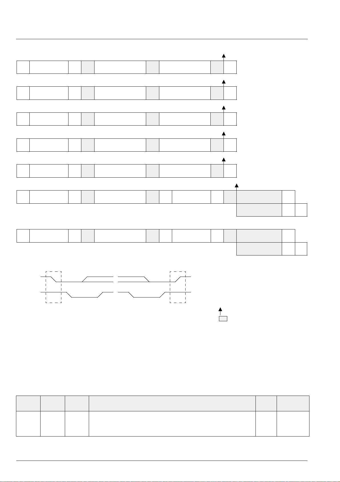
VCT 38xxA ADVANCE INFORMATION
SAckWAckAckP0010001
SAckWAck
0010001
SAckWAck
0010001
SAckWAck
0010001
SAckWAck
0010001
SAckWAckS
0010001
0111 1000
0111 1001
0111 1010
0111 1011
0111 1100
0111 1100 0010001
n Byte Sub 1
n Byte Sub 2
n Byte Sub 3
n Byte Sub 4
n Byte Data
Ack P
Ack P
Ack P
Ack P
Ack
R
n
−1 Byte Data
last Byte Data
Ack
Nak
SAckWAckS
0010001
SDA
0111 1101
1
0
0010001 Ack
PS
SCL
R
W
R
Ack
Nak
S
P
Fig. 3–21: I2C bus protocol
3.14.1.5. Hardware Identification
A separate I
2
C bus slave register is reserved to read
out the hardware version of VCT 38xxA. This register
is active in standby mode.
I2C Sub
address
Number
of bits
Mode Function Default Name
Ack
Status
Status
0
=
1
=
0
=
1
=
Start
=
Stop
=
=
Interrupt
=
Data from TPU
NakPP
h’9F 16 r Hardware version number
bit[7:0] hardware id (A3=h’13, B1=h’21 a.s.o.)
bit[15:8] product code VCT38xy (VCT3832=h’32)
read
only
HWID
TC
PROD
84 Micronas
Page 85
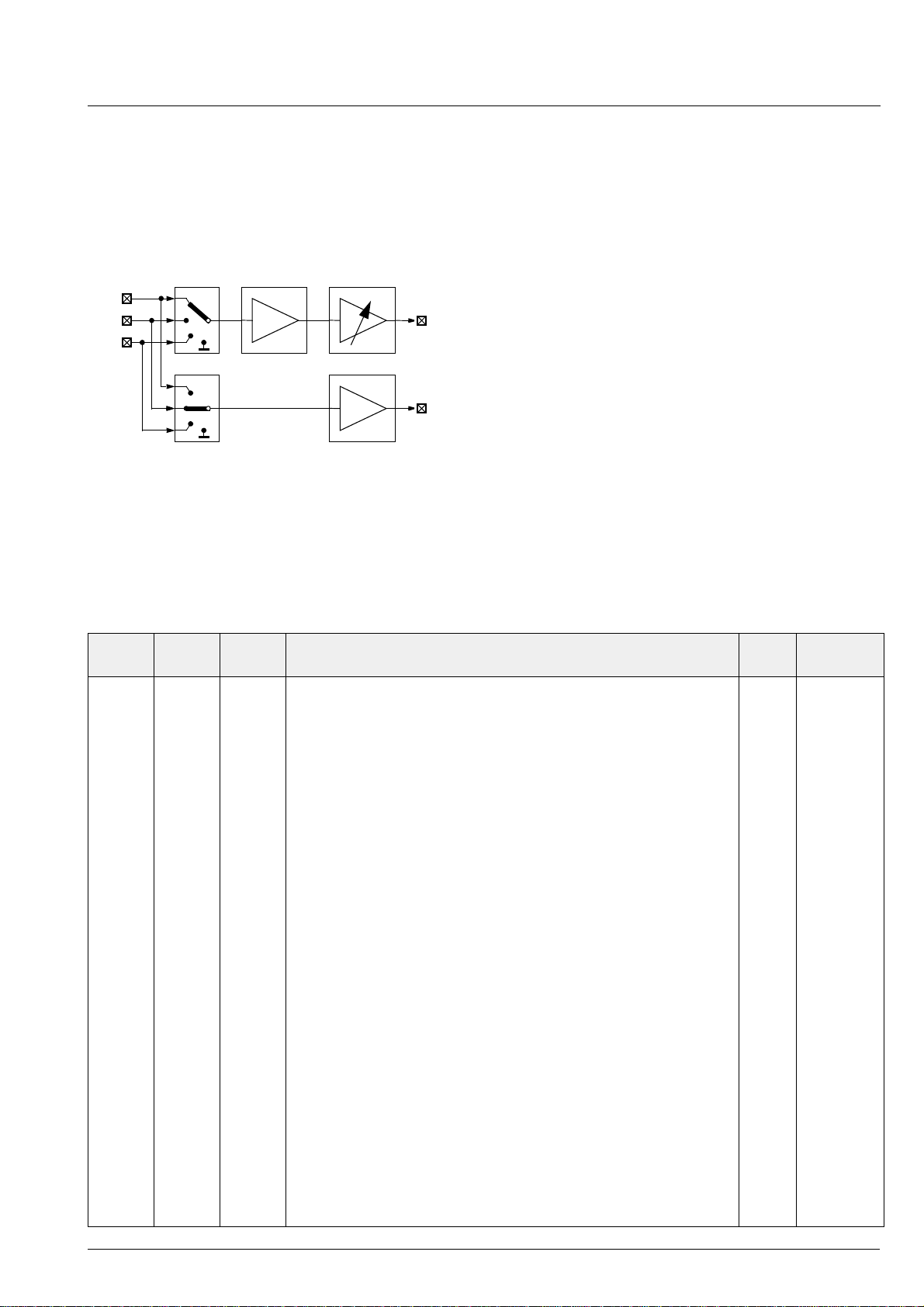
ADVANCE INFORMATION VCT 38xxA
4. Audio Processing
4.1. Introduction
The audio processing allows input selection and volume control for mono audio sources either from tuner
or from SCART input.
AIN1
AIN2
AIN3
AOUT1
AOUT2
Fig. 4–1: Audio processing
Table 4–1: Audio control register
4.2. Input Select
Both audio output channels can be switched to any of
the three audio input channels. Only the audio output
channel AOUT1 can be volume controlled.
4.3. Volume Control
The analog volume control covers a range from
+18 dB and
−75 dB. The lowest step is the mute posi-
tion. Step size is split into a 3-dB and a 1.5-dB range.
−75 dB...−54 dB : 3 dB step size
−54 dB...+18 dB : 1.5 dB step size
2
4.4. I
C-Bus Slave Interface
The input selection and analog volume is controlled via
the audio control register ACON. This I
2
C register is
activated by the chip address of the video back-end
processing (see Table 2–2 on page 32).
I2C Sub
address
Number
of bits
Mode Function Default Name
h’34 16 w Audio Control
bit [5:0] volume control
bit [7:6] reserved
bit [9:8] audio input select 1
bit [11:10] audio input select 2
bit[12] low power mode
bit[15:13] reserved
000000 mute
000001
−75db
...
000111
001000
−57.0dB
−54.0dB
...
101011
−1.5dB
101100 0.0dB
101101 +1.5dB
...
110110 +15.0dB
110111 +16.5dB
111000 +18.0dB
00 mute
01 AIN1
10 AIN2
11 AIN3
00 mute
01 AIN1
10 AIN2
11 AIN3
0 disable low power mode
1 enable low power mode
0ACON
AVOL
ASEL1
ASEL2
ALPM
Micronas 85
Page 86
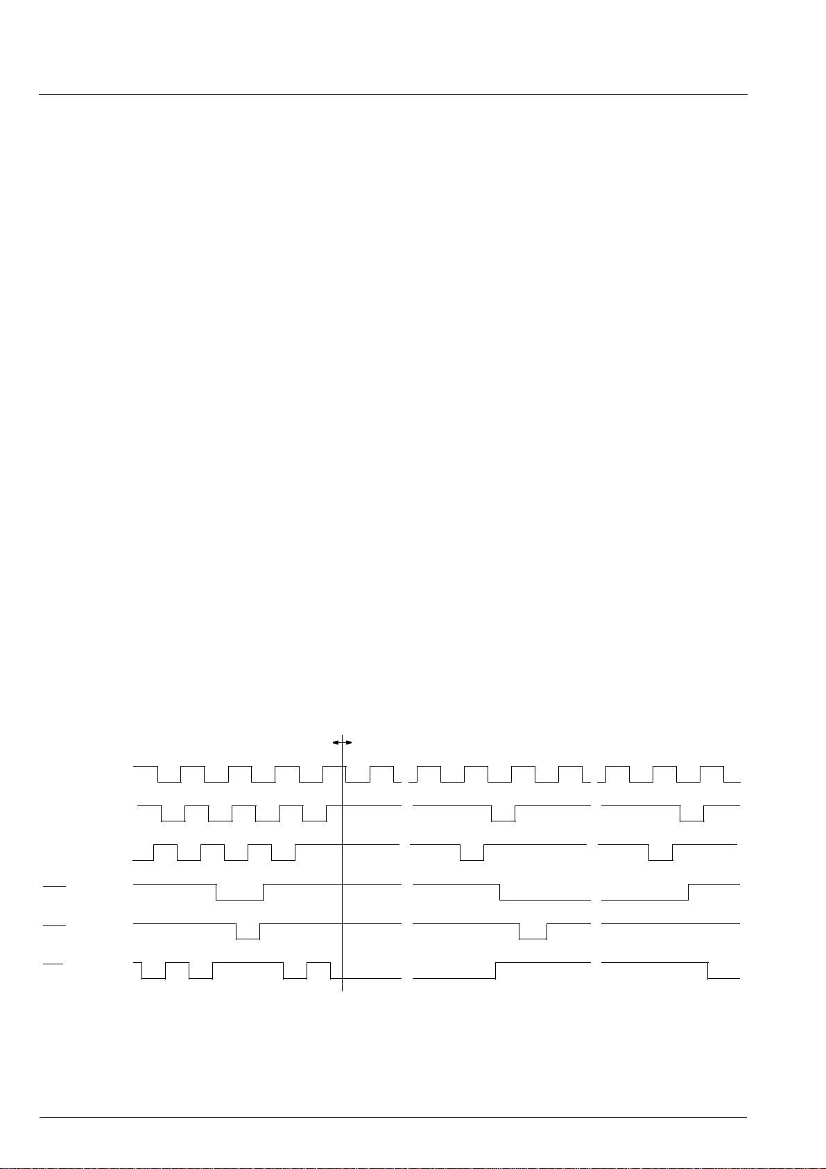
VCT 38xxA ADVANCE INFORMATION
5. TV Controller
5.1. Introduction
The TV controller basically consists of the CPU, RAM,
ROM, and a number of peripheral modules.
For instance:
– a memory banking module is included to allow
access to more than 64 kB memory.
– a bootloader software is included to allow in-system-
downloading of external code to Flash memory via
2
C interface.
the I
The TV controller runs the complete software necessary to control a TV set. The software includes control
of the audio, video, OSD, and text processors on chip,
as well, as control of external devices like tuner or stereo decoder.
Communication between the TV controller and external devices is done either via I
2
C bus interface or via
programmable port pins.
The TV Controller is clocked with f
OSC
= f
XTAL
/2.
5.2.1. CPU Slow Mode
To reduce power consumption considerably, the user
can reduce the internal CPU clock frequency to 1/256
of the normal f
value. In this CPU Slow mode, pro-
CPU
gram execution is reduced to 1/256 of the normal
speed, but clocking of most other modules remains
unaffected. The modules that are affected by CPU
Slow mode are:
1. CPU and Interrupt Controller with all internal and
external interrupts
2. RAM, ROM and DMA
3. Watchdog
Some modules must not be operated during CPU Slow
mode. Refer to module sections for details.
After reset the CPU is in Fast mode (f
CPU
= f
OSC
).
CPU Slow mode is enabled by clearing flag CPUFST
in standby register SR1. The CPU clock frequency
reduction to f
delay of 256 f
/256 will take effect after a maximum
OSC
periods.
OSC
5.2. CPU
The CPU is fully compatible to WDC’s W65C02 microprocessor. The processor has 8-bit registers/accumulator, an 8-bit data bus, and a 16-bit address bus. For
further information about the CPU core, please refer to
the WDC W65C02 data sheet.
fast mode
f
OSC
PH2
CCUPH2
RW
WE
Returning CPU to Fast mode is done by setting flag
CPUFST to High. The CPU clock frequency will immediately change to its normal f
Fig. 5–1 shows the memory access signals during
CPU fast and slow mode.
slow mode
OSC
value.
OE
Fig. 5–1: Memory access signals
86 Micronas
Page 87

ADVANCE INFORMATION VCT 38xxA
5.3. RAM and ROM
On-chip RAM is composed of static RAM cells. The
RAM will hold all information during reset, as long as
the specified operating voltages are available.
The 64PSDIP Multi Chip Module contains a 128-KByte
Flash EEPROM of the ST M29W010B type. These
devices exhibit electrical Byte program and block erase
functions. Refer to the ST M29W010B data sheet for
details.
5.3.1. Address Map
The following ROM addresses are reserved and cannot be used to store program code.
Table 5–1: Reserved (physical) addresses
Addresses Usage
00FFC6
− 00FFD5
00FFD6 − 00FFD7
00FFD8 − 00FFF7
00FFF8
00FFF9
00FFFA − 00FFFB
00FFFC − 00FFFD
0xFFFE − 0xFFFF
Manufacturer ROM ID
reserved for bootloader
Interrupt Vectors
reserved
Control Word (during reset)
NMI Vector (expanded by
Interrupt Controller)
Reset Vector
IRQ/BRK Vector
A 16-Byte address space is reserved as “Manufacturer
ROM ID”. This area contains a unique ROM ID number
which has to be agreed between Micronas and the
customer. Especially the first 6 digits identify customer
and version. As an example a Micronas demo software
is identified like “MI1108 240700 TV”.
Tabl e 5 –2 shows the internal memory segmentation.
Internal program RAM and ROM can be disabled via
the Control Register (chapter 5.4. on page 87). The
internal text RAM can be disabled via Standby Register 0 (see page 89).
All memory locations not available internally will be
addressed as external memory. It is possible to operate with internal and external memory in parallel, but
overlapping memory segments will always be
addressed internally.
Table 5–2: Internal Memory Locations
Addresses Internal Memory
000000
− 000FFF
001E00 − 001FFF
002000 − 0023FF
002400 − 019FFF
0A0000 − 0A3FFF
4k Program RAM
I/O Register
1k Bootloader ROM
95k Program ROM
16k Text RAM
5.3.2. Bootloader
A segment of the internal ROM is reserved for bootloader code. Via this bootloader code it is possible to
download additional code into the internal RAM and
execute this code. The downloaded code can be used
to program the external Flash EEPROM.
2
After reset the bootloader checks the I
C bus pins SDA
and SCL for a special identification sequence. If no
identification sequence is detected, the bootloader
starts the application program code.
The bootloader checks the address FFD6/FFD7 of the
external memory if there is a predefined pattern
(A55Ah). If so, it starts the external application software else it starts the internal application software.
5.4. Control Register
The Control Register CR serves to configure the ways,
by which certain system resources are accessed during operation. The main purpose is to obtain a variable
system configuration during IC test.
Upon each High transition on the RESQ pin internal
hardware reads data from address location 00FFF9h
and stores it to the CR. The state of the TEST pin at
this timepoint specifies which program storage source
is accessed for this read:
– With the TEST pin Low, the control byte is read from
internal program storage (mask ROM). With location
00FFF9h set to FFh, this is the setting for standalone operation.
– With the TEST pin High, the control byte is read
from external memory via the test bus (for test purposes only).The system will thus start up according
to the configuration defined in address location
00FFF9h and automatically copied to register CR.
During internal memory access, the pins DB0-DB7,
WExQ and OExQ are tristate. For emulation and test
purposes it is possible to change this behavior via the
Micronas 87
Page 88
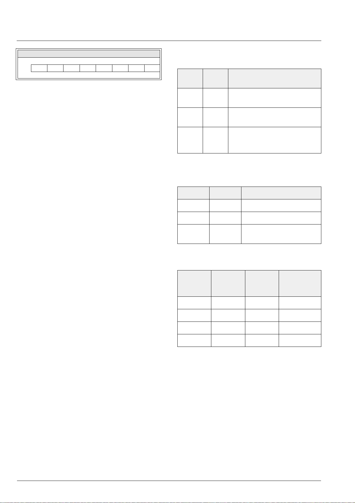
VCT 38xxA ADVANCE INFORMATION
1: 1F01 2: CR 3: Control Register
bit76543210
r/w RESLNG TSTTOG DISEXT MFM TSTROM IROM IRAM ICPU
reset Value of 00FFF9h
RESLNG Reset Pulse Length
OSC
OSC
.
.
r/w1: Pulse length is 4095/f
r/w0: Pulse length is 16/f
This bit specifies the length of the reset pulse which is
output at pin RESQ following an internal reset. If pin
TEST is 1 the first reset after power on is short. The
following resets are as programmed by RESLNG. If pin
TEST is 0 all resets are long.
TSTTOG TEST Pin Toggle
r/w1: Pin TEST can toggle the Multi Function
pins.
r/w0: Pin TEST can’t toggle the Multi Function
pins.
This bit is used for test purposes only. If TSTTOG is
true in IC active mode, pin TEST can toggle the Multi
Function pins between Bus mode and normal mode.
Table 5–5: Some commonly used settings for address
location 00FFF9h.
Code TEST
Operation Mode
Pin
FFh 0 Stand-alone with internal ROM
or Flash
DFh 0 Emulator mode (CPGA257
package)
ABh 1 External program storage con-
nected to Multi Function pins in
Bus mode
Table 5–3: TSTROM and IROM usage in mask ROM
parts
TSTROM IROM selected program storage
1 1 internal CPU ROM
0 1 internal Test ROM
DISEXT Disable External Memory Access
r/w1: DB0
−DB7, WExQ and OExQ output pins
are tristate during internal memory
access (see Fig. 5–2 on page 89).
r/w0: DB0
−DB7, WExQ and OExQ output pins
are active during internal memory access.
MFM Multi Function pin Mode
r/w1: Enable normal mode.
r/w0: Enable Test Bus mode.
TSTROM Test ROM (mask ROM parts only)
r/w1: Disable internal Test ROM.
r/w0: Enable internal Test ROM (@ IROM=1).
IROM Internal ROM
r/w1: Enable internal CPU ROM.
r/w0: Disable internal CPU ROM.
IRAM Internal RAM
r/w1: Enable internal CPU RAM.
r/w0: Disable internal CPU RAM.
ICPU Internal CPU
r/w1: Enable internal CPU.
r/w0: Disable internal CPU.
x 0 external on Multi Function
pins in Bus mode
Table 5–4: TSTTOG and MFM usage
TSTTOG MFM TEST pin Multi
Function
Pins
x 1 x normal mode
1 0 1 normal mode
100Bus mode
0 0 x Bus mode
88 Micronas
Page 89
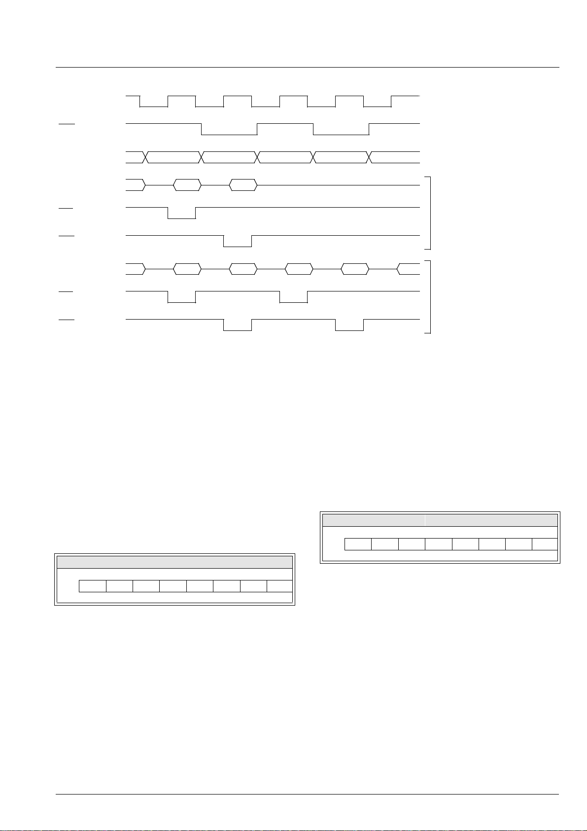
ADVANCE INFORMATION VCT 38xxA
PH2
RW
ADB
extern extern
DB
OE
WE
DB
OE
WE
Fig. 5–2: Internal/external memory access
5.5. Standby Registers
internal signal
internal signal
intern intern
Controlword
DISEXT= 1
Controlword
DISEXT= 0
The Standby registers allow the user to switch on/off
power or clock supply of single modules. With these
flags it is possible to greatly influence power consumption and its related electromagnetic interference.
For details about enabling and disabling procedures
and the standby state refer to the specific module
descriptions.
The minimum IC current consumption is obtained with
all standby registers set to 00h.
4: 1F08 5: SR0 6: Standby Register 0
bit76543210
r/w PWM1 PWM0 TRAM CCC TVPWM
reset00000000
PWM1 Pulse Width Modulator 1
r/w1: Module active.
r/w0: Module off.
PWM0 Pulse Width Modulator 0
r/w1: Module active.
r/w0: Module off.
CCC Capture Compare Counter
r/w1: Module active.
r/w0: Module off.
TVPWM Tuning Voltage Pulse Width Modulator
r/w1: Module active.
r/w0: Module off.
7: 1F09 8: SR1 9: Standby Register 1
bit76543210
r/w CPUFST ADC TIM1 TIM0
reset01000000
CPUFST CPU Fast Mode
r/w1: Fast mode: f
r/w0: Slow mode: f
CPU
CPU
= f
= f
XTAL
XTAL
/ 2
/ 512
ADC ADC Module
r/w1: Module active.
r/w0: Module off.
TIM1 Timer 1
r/w1: Module active.
r/w0: Module off.
TRAM Text RAM
r/w1: Module active
r/w0: Module off
TIM0 Timer 0
r/w1: Module active.
r/w0: Module off.
Micronas 89
Page 90

VCT 38xxA ADVANCE INFORMATION
10: 1F0A 11: SR2 12: Standby Register 2
bit76543210
r/w PWM3 PWM2 I2C MB
reset00000000
PWM3 Pulse Width Modulator 3
r/w1: Module active.
r/w0: Module off.
PWM2 Pulse Width Modulator 2
r/w1: Module active.
r/w0: Module off.
2
I2C I
C-Bus Master Interface
r/w1: Module active.
r/w0: Module off.
MB Memory Banking
r/w1: Module active.
r/w0: Module off.
5.6. Test Registers
Test registers are for manufacturing test only. They
must not be written by the user with values other than
their reset values (00h). They are valid independent of
the TEST input state.
In all applications where a hardware reset may not
occur over long times, it is good practice to force a
software reset on these registers within appropriate
intervals.
22: 1FFC 23: TST4 24: Test Register 4
bit76543210
w For testing purposes only
reset00000000
25: 1FFB 26: TST5 27: Test Register 5
bit76543210
r For testing purposes only
reset00000000
5.7. Reset Logic
5.7.1. Alarm Function
An alarm comparator on the pin RESQ allows the
detection of a threshold higher than the reset threshold. An alarm interrupt can be triggered with the output
of this comparator.
The interrupt source output of this module is routed to
the Interrupt Controller logic. But this does not necessarily select it as input to the Interrupt Controller.
Check section “Interrupt Controller” for the actually
selectable sources and how to select them.
The intended use of this function is made, when a system uses a 3.3V regulator with an unregulated input. In
this case, the unregulated input, scaled down by a
resistive divider, is fed to the RESQ pin. With falling
regulator input voltage this alarm interrupt is triggered
first. Then the reset threshold is reached and
VCT 38xxA is reset before the regulator drops out.
13: 1FFE 14: TST1 15: Test Register 1
bit76543210
w For testing purposes only
reset00000000
16: 1FFF 17: TST2 18: Test Register 2
bit76543210
w For testing purposes only
reset00000000
19: 1FFD 20: TST3 21: Test Register 3
bit76543210
w For testing purposes only
reset00000000
The time interval between the occurrence of the alarm
interrupt and the reset may be used to save process
data to nonvolatile memory. In addition, power saving
steps like turning off other devices may be taken to
increase the time interval until reset. The alarm interrupt is a level triggered interrupt. The interrupt is active
as long as the voltage on pin RESQ remains between
the two thresholds of alarm and reset (see Fig. 5–3 on
page 92).
5.7.2. Software Reset
The TV controller software can generate a reset via
the Reset Control Register (see page 94). To prevent
the TV controller from carrying out a reset in this case,
the internal CPU reset can be disconnected from the
RESQ pin.
90 Micronas
Page 91

ADVANCE INFORMATION VCT 38xxA
5.7.2.1. From Standby into Normal Mode
To switch the whole TV application from standby operation into normal mode the controller has to perform
the following sequence:
– RC.RESDIS = 1, RC.DCOCLP = 1
– RC.RESOUT =1
– switch on power supply
– wait for stable power supply
– RC.SELCLK = 1, RC.I2CEN = 1
– RC.DCOCLP = 0, RC.RESOUT = 0
– wait for RC.ALI = 0 (ext. capacitor!)
– RC.RESDIS = 0
– init DMA interface
– init TPU, VDP and Audio
– init external devices
5.7.2.2. From Normal into Standby Mode
To switch the whole TV application from normal mode
into standby operation the controller has to perform the
following sequence:
– RC.DCOCLP = 1, RC.I2CEN = 0
– wait 1ms for stable 20.25MHz DCO
– RC.SELCLK = 0
– turn off power supply
– set TPU into standby mode
– SR0 = 2, SR1 = 8, SR2 = 0
5.7.3. Internal Reset Sources
The VCT 38xxA contains three internal circuits that are
able to generate a system reset: watchdog, supply
supervision, and clock supervision.
All internal resets are directed to the open drain output
of pin RESQ. Thus a “wired or” combination with external reset sources is possible. The RESQ pin is current
limited and therefore large external capacitances may
be connected.
All internal reset sources initially set a reset request
flag. This flag activates the pull-down transistor on the
RESQ pin. An internal reset prolongation counter
starts, as soon as no internal reset source is active any
more. It counts 4096 f
periods (for alternative set-
CPU
tings refer to register CR) and then resets the reset
request flag, thus releasing the RESQ pin.
Micronas 91
Page 92
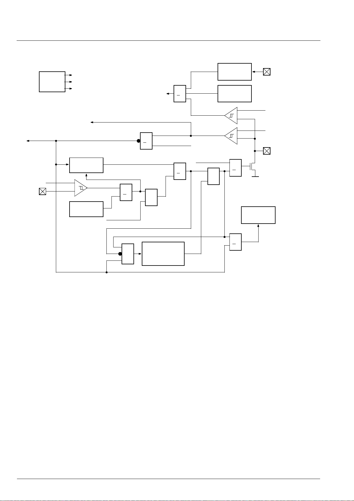
VCT 38xxA ADVANCE INFORMATION
CPU Reset
V
REFPOR
VSUP
S
Bandgap
V
REFA
V
REFR
V
REFPOR
Watchdog
+
-
Clock
Supervision
RESET
Interrupt
Source
internal Reset to DMA, TPU, VDP
>1
RC.RESDIS
>1
CSW0.CSA
&
&
Reset extension
16 or 4096
oscillator pulses
>1
>1
RC.VSI
RC.TPUI
RC.ALI
RC.RESOUT
SQ
R
Voltage
Supervision
TPU
Watchdog
+
-
+
-
>1
reset
>1
Reset
Control
V
V
RC
VSUP
REFA
REFR
RESQ
D
Fig. 5–3: Block diagram of reset logic
5.7.3.1. Supply Supervision
An internal bandgap reference voltage is compared to
VSUP
. A VSUPS level below the Supply Supervision
S
threshold VREFPOR will permanently pull the pin
RESQ low and thus hold the VCT 38xxA in reset state
(see Fig. 5–3 on page 92). This reset source is active
after reset and can be enabled/disabled by flag CSA in
register CSW0.
5.7.3.2. Clock Supervision
The Clock Supervision monitors the CPU clock frequency f
. A frequency level below the clock super-
CPU
vision threshold of approx. 200 kHz will permanently
pull the pin RESQ low and thus hold the IC in reset
(see Fig. 5–3 on page 92). This reset source is active
after reset and can be enabled/disabled by flag CSA in
register CSW0.
A frequency exceeding the specified clock frequency is
not detected.
92 Micronas
Page 93
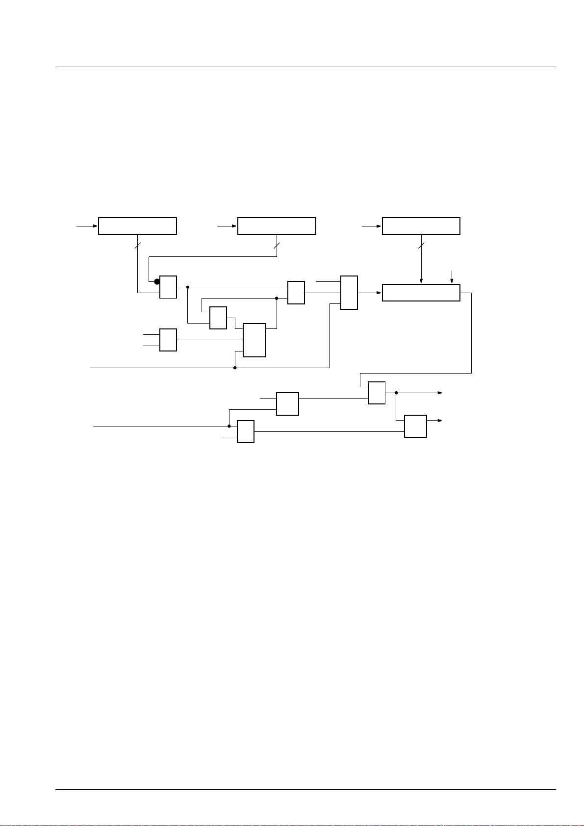
ADVANCE INFORMATION VCT 38xxA
5.7.3.3. Watchdog
The Watchdog module serves to monitor undisturbed
program execution. A failure of the program to retrigger
the Watchdog within a preselectable time will pull the
RESQ pin low and thus reset the VCT 38xxA (see Fig.
Once the Watchdog is enabled, it cannot be disabled anymore, neither by software nor by pulling
down the external RESQ pin. Only after power up
the watchdog is disabled.
5–3 and Fig. 5–4). The Watchdog reset source is only
enabled after the first write access to register CSW1
(see Section 5.7.3.2. on page 92).
2.write 3.write
& even & odd
reset in
power on
Trigger Reg1 Timer RegisterTrigger Reg2
8
=
&
Q
2.write & even
3.write & odd
≥1
write CSW1
D
C
S
1. write
≥1
CSW1CSW1
1. write
8 8
1. write
&
SQ
R
≥1
load
8-Bit-Counter
&
SQ
R
CSW1
clk = f
reset out
CSW1.WDRES
CPU
/8192
zero
Fig. 5–4: Block diagram of watchdog
The Watchdog contains a down-counter that generates a reset when it wraps from zero to FFh. It is
reloaded with the content of the watchdog timer register, when, on a write access to register CSW1, watchdog trigger registers 1 and 2 contain bit complemented
values. Resetting the VCT 38xxA initializes the watchdog timer register to FFh, thus forcing the Watchdog to
create a maximum reset interval.
The Watchdog is controlled by register CSW1. The
first write access to it loads the timer register value setting the Watchdog’s unretriggered reset interval. The
desired interval can be programmed by setting the
CSW1 value to:
Value
Interval f
------------------------------------1–=
8192
×
CPU
The resolution of the Watchdog is 8192/f
CPU
. In CPU
Slow mode (see Section 5.2.1. on page 86), the watchdog is clocked with the reduced CPU clock.
The second and all following even numbered write
accesses load watchdog trigger register 1, the third
and all following odd numbered write accesses load
watchdog trigger register 2.
In all future, the CPU has to write alternatingly to register CSW1 value and bit complement value, thus retriggering the up-counter. Failure to retrigger will result in
an overflow of the up-counter generating a Watchdog
reset.
It is not allowed to change a chosen value. Writing a
wrong value to CSW1 immediately sets the flag
CSW1.WDRES and prohibits further retriggering of the
watchdog counter.
CSW1.WDRES is true after a Watchdog reset. Only a
Supply Supervision reset or a write access to register
CSW1 clears it.
Micronas 93
Page 94
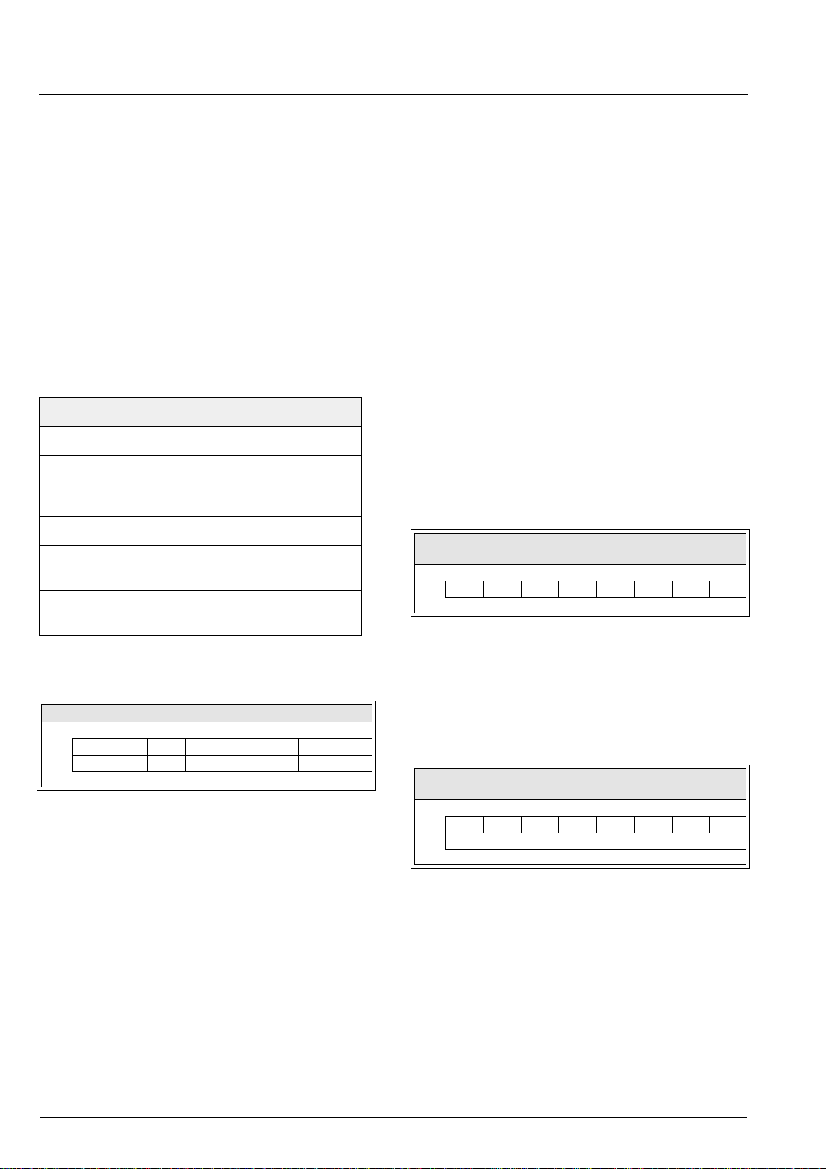
VCT 38xxA ADVANCE INFORMATION
5.7.4. External Reset Sources
As long as the reset input comparator on the pin
RESQ detects the Low level, the VCT 38xxA is in reset
state. On this pin, external reset sources may be wireored with the internal reset sources, leading to a system-wide reset signal combining all system reset
sources.
5.7.5. Summary of Module Reset States
After reset, the controller modules are set to the following reset states:
Table 5–6: Status after reset
Module Status
CPU CPU Fast mode.
Interrupt
Controller
Interrupts are disabled. Priority registers, request flip-flops and stack
are cleared.
If the source of one of these interrupts is still active,
resetting the interrupt flag will not work and no further
interrupt will be generated.
I2CEN I2C Enable
r/w1: Enable I2C output from FE/BE.
r/w0: Disable I2C output.
DCOCLP DCO clamping
r/w1: DCO input clamped to 0.
r/w0: DCO input controlled by front-end.
SELCLK Select clock source
r/w1: From PLL.
r/w0: From DCO.
RESDIS Reset Disable
r/w1: Disable internal CPU reset.
r/w0: Enable internal CPU reset.
RESOUT RESQ Output
w1: RESQ output active.
w0: RESQ output inactive.
Ports Normal mode. Output is tristate.
Watchdog Switched off. SW activation is pos-
sible.
Clock
monitor
EMU IC: Active. SW may toggle.
normal IC: Permanently active.
5.7.6. Reset Registers
28: 1F07 29: RC 30: Reset Control Register
bit76543210
w ALI VSI TPUI I2CEN DCOCLP SELCLK RESDIS RESOUT
r ALI VSI TPUI I2CEN DCOCLP SELCLK RESDIS 0
reset00001000
This register controls the reset logic and clock generation.
ALI Alarm Interrupt
r1: Alarm was interrupt source
r0: no pending alarm interrupt
w1: reset alarm interrupt
31: 1F00 32: CSW0 33: Clock, Supply & Watchdog Regis-
ter 0
bit76543210
w xxxxxxxCSA
resetxxxxxxx1
This register controls the Supply and Clock Supervision modules.
CSA Clock and Supply Supervision Active
w1: Both Enabled.
w0: Both Disabled.
34: 1F60 35: CSW1 36: Clock, Supply & Watchdog Regis-
ter 1
bit76543210
r xxxxxxxWDRES
w Watchdog Time and Trigger Value
reset11111111
This register controls the Watchdog module. Only values between 1 and 255 are allowed.
VSI VSUP
r1: VSUP
r0: no pending VSUP
w1: reset VSUP
Voltage Supervision Interrupt
D
supervision was interrupt source
D
D
supervision interrupt
D
supervision interrupt
TPUI TPU Watchdog Interrupt
r1: TPU watchdog was interrupt source
r0: no pending TPU watchdog interrupt
w1: reset TPU interrupt flag
WDRES Watchdog Reset Source
r1: Watchdog was reset source.
w: Any write access to CSW1 resets this
flag.
First write the desired watchdog time value to this register. On further writes, to retrigger the Watchdog,
alternatingly write a value (not necessarily the former
time value) and its bit complemented value. Never
change the latter value.
94 Micronas
Page 95
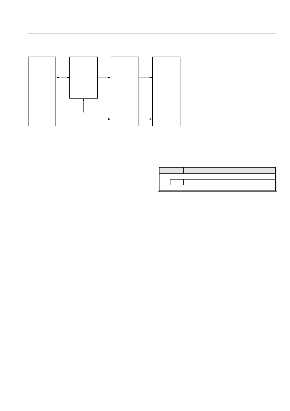
ADVANCE INFORMATION VCT 38xxA
5.8. Memory Banking
*D0 ... D7
Banking
Register
A15 ... A19
Interrupt
65C02
Controller,
DMA
Logic
*A15
*A0 ... A14
*Processor internal Bus
A0 ... A14
Fig. 5–5: Block diagram of Memory Banking
The 8-bit processor W65C02 only allows access to
64 kByte of memory space. To allow access to the
expanded memory range above 64 kByte, a specific
banking hardware is implemented. The physical
address range above 32 kBytes (A15 = 1) is separated
into several banks of which only one at a time is
enabled and selected by the Banking register (BR),
which is programmable as any other standard peripheral register by writing the desired value into its specific address. The content of the BR is also readable,
so the software may check the current bank at any
time. The applied software is responsible to program
the BR with the correct bank number at the right time.
Since the upper 32 kBytes range is switched immediately after programming the BR, correct function is not
guaranteed if it is changed by a program sequence
running in a switched bank. BR settings need to be
done in the lower 32 kBytes (A15 = 0), which is the
non-switchable master bank (bank 0).
A15 ... A19
Address
Decoder,
Memory,
I/O
A0 ... A14
5.8.1. Banking Register
37: 1F0F 38: BR 39: Banking Register
bit76543210
r/w BN
reset00000001
BN Bank Number
r/w: number of 32 kByte memory bank
Setting BN = 0 should be avoided because it will mirror
the non-switchable master bank (bank 0) into the
upper 32-kByte area (A15 = 1). RAM, I/O pages and
reserved addresses may be manipulated unintentionally.
RESET initializes BN = 1 to read control byte and reset
vector from bank 1. Also, interrupt vectors have to
reside in bank 1, because the Interrupt Controller generates the appropriate address of bank 1, but it does
not change the contents of the BR. Interrupt functions
have to reside in the non-switchable master bank
(bank 0). Otherwise,they need to be in each used
bank, because after getting the vector the unchanged
contents of the BR determine the current bank which is
valid if A15 is “1”.
Micronas 95
Page 96
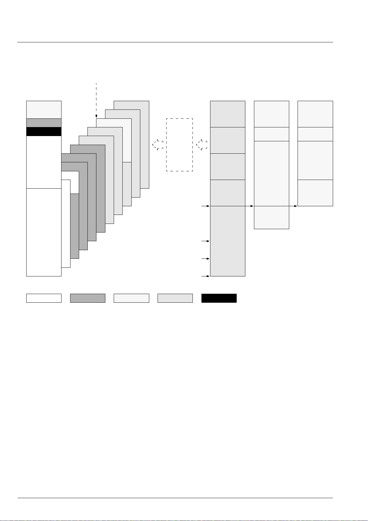
VCT 38xxA ADVANCE INFORMATION
CPU RAM/ROM Text RAM TPU Address Space
000000H
000FFFH
reserved
001E00H
002000H
008000H
00FFFFH
Bank 0Bank 1
078000H
Bank 3
Bank 2
088000H
080000H
084000H
Bank 5-14
Bank 4
087FFFH
0A8000H
0A0000H
Bank 16
Bank 15
0F8000H
Bank 20
Bank 17-19
Bank 21-30
Bank 31
DMA
128kbyte
256kbyte
512kbyte
16kbyte
≥128k Text RAM
000000H
Page
Ta b le
001000H
Scratch
002000H
TTX
Bank
003000H
OSD
Bank
004000H
Page
Memory
020000H
040000H
07FFFFH
19k Text RAM
000000H
Page
Ta bl e
001000H
Scratch
001800H
Page
Memory
004000H
OSD&TTX
Bank
16k Text RAM
000000H
Page
Ta bl e
001000H
Scratch
001800H
Page
Memory
003000H
OSD&TTX
Bank
int. ROM
ext. RAMint. RAMext. ROM
I/O-Reg
Fig. 5–6: Memory Banking shown with the maximal size of addressable memory
5.9. DMA Interface
The DMA interface connects the TPU SRAM interface
to the CPU memory bus (see Fig. 5–7). This is done to
avoid extra pins for external TPU page memory.
As long as the DMA interface is disabled, the TPU cannot access the CPU address bus and therefore should
not transfer data to/from the internal/external SRAM.
To ensure this, the controller should reset the TPU
The DMA interface must not be operated during CPU
Slow mode. The DMA interface can be disabled via
DMAIM.DMAEN.
before disabling the DMA interface. After reset the
TPU will not access the memory until receiving the I
command “DRAM_MODE” (see Section 3.12. on
page 68).
2
C
96 Micronas
Page 97
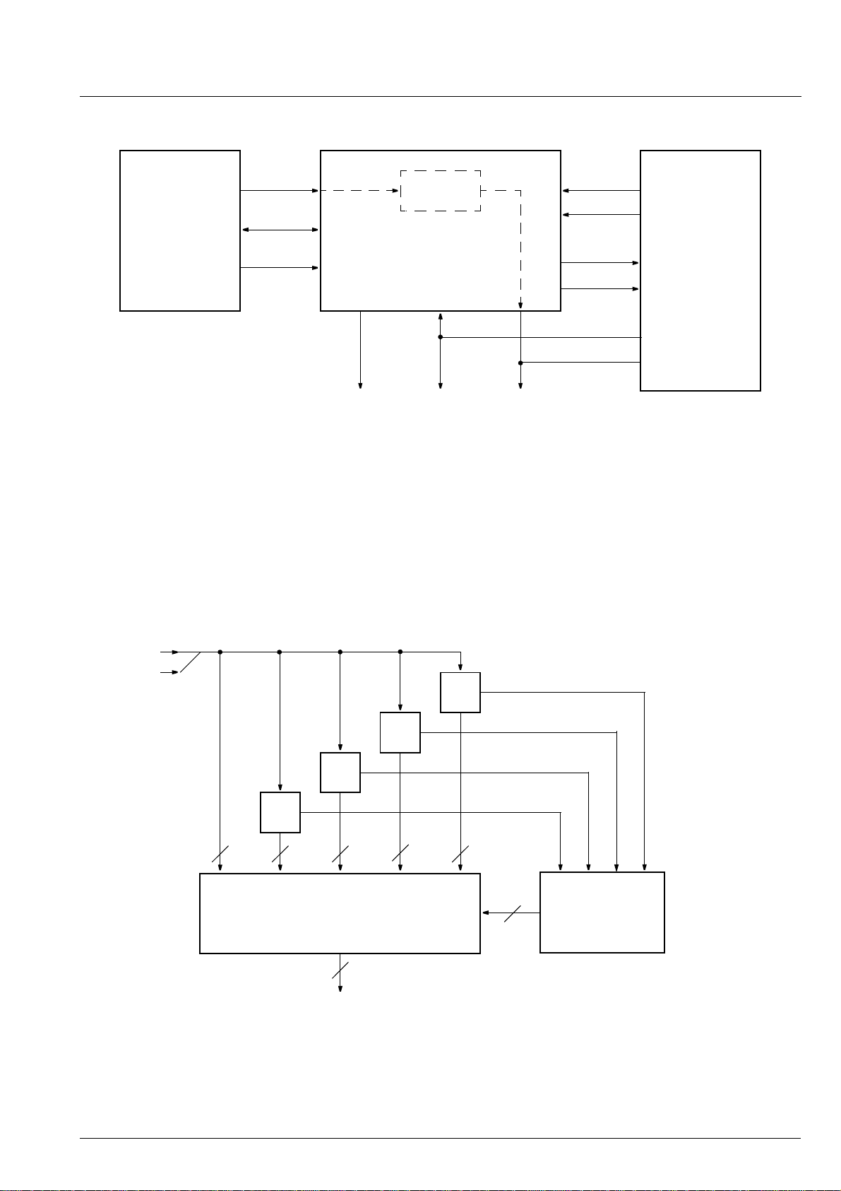
ADVANCE INFORMATION VCT 38xxA
A[18:0]
TPU
SRAM
D[7:0]
DMA Interface
Interface
RWQ
Fig. 5–7: Block diagram of DMA interface
In general, all TPU addresses are mapped into bank
16 to 31 of the CPU address space by forcing the MSB
of the address bus to “1” (see Fig. 5–8). Additionally
4 memory segments can be mapped into any address
area by programming a set of DMA registers (see
Fig. 5–9).
Address
Mapping
PH2
RWQ
RDY
BE
CPU
ADB[19:0]DB[7:0]RWQ
Special care should be taken when mapping TPU
addresses into the RAM area of bank 0. Any overlap between TPU memory (e.g. OSD Bank) and
controller memory (e.g. non zero page variables)
must be avoided.
A[18:8]
TPU Address Bus
A19 = “1”
map
1
12 12
Fig. 5–8: DMA address mapping
map
2
Mux 1:5
12
ADB[19:8]
map
3
12
map
4
1212
match4
match3
match2
match1
3
Decoder
Micronas 97
Page 98
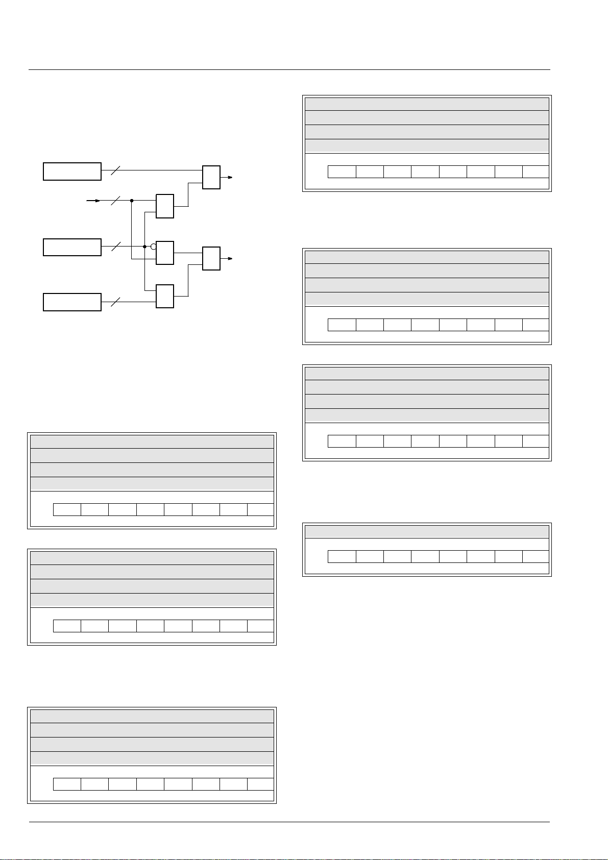
VCT 38xxA ADVANCE INFORMATION
&
=
≥1
MASK n
CMP n
MAP n
match
&
&
A[19:8]
A[19:8]
n: mapping logic 1 to 4
12
12
12
12
If the mapping logic does not find any address match,
the TPU address is directly put on the CPU address
bus with A19 set to “1”. In case of multiple matches,
the priority is map1 > map2 > map3 > map4.
76: 1E0C 77: CMP1H 78: Compare 1 High Byte
79: 1E0D 80: CMP2H 81: Compare 2 High Byte
82: 1E0E 83: CMP3H 84: Compare 3 High Byte
85: 1E0F 86: CMP4H 87: Compare 4 High Byte
bit76543210
w CA19 CA18 CA17 CA16
reset 1 1 1 1
CA19 to 8 Compare Address
Masked TPU address is compared with this value.
88: 1E10 89: MAP1L 90: Map 1 Low Byte
91: 1E11 92: MAP2L 93: Map 2 Low Byte
94: 1E12 95: MAP3L 96: Map 3 Low Byte
97: 1E13 98: MAP4L 99: Map 4 Low Byte
bit76543210
w MPA15 MPA14 MPA13 MPA12 MPA11 MPA10 MPA9 MPA8
reset11111111
Fig. 5–9: DMA mapping logic
5.9.1. DMA Registers
40: 1E00 41: MASK1L 42: Mask 1 Low Byte
43: 1E01 44: MASK2L 45: Mask 2 Low Byte
46: 1E02 47: MASK3L 48: Mask 3 Low Byte
49: 1E03 50: MASK4L 51: Mask 4 Low Byte
bit76543210
w MA15 MA14 MA13 MA12 MA11 MA10 MA9 MA8
reset11111111
52: 1E04 53: MASK1H 54: Mask 1 High Byte
55: 1E05 56: MASK2H 57: Mask 2 High Byte
58: 1E06 59: MASK3H 60: Mask 3 High Byte
61: 1E07 62: MASK4H 63: Mask 4 High Byte
bit76543210
w MA19 MA18 MA17 MA16
reset 1 1 1 1
MA19 to 8 Mask Address
TPU address is masked with this value.
100: 1E14 1 01: MAP1H 102: Map 1 High Byte
103: 1E15 1 04: MAP2H 105: Map 2 High Byte
106: 1E16 1 07: MAP3H 108: Map 3 High Byte
109: 1E17 1 10: MAP4H 111: Map 4 High Byte
bit76543210
w MPA19 MPA18 MPA17 MPA16
reset 1 1 1 1
MPA19 to 8 Map Address
Matching TPU address is replaced with this value.
112: 1E18 113: DMAIM 114: DMA Interface Mode
bit76543210
w DMAEN MAP4E MAP3E MAP2E MAP1E
reset0 0000
DMAEN DMA Enable
w1: Enable DMA Interface
w0: Disable DMA Interface
MAPxE Mapping Logic x Enable
w1: Enable mapping logic x
w0: Disable mapping logic x
64: 1E08 65: CMP1L 66: Compare 1 Low Byte
67: 1E09 68: CMP2L 69: Compare 2 Low Byte
70: 1E0A 71: CMP3L 72: Compare 3 Low Byte
73: 1E0B 74: CMP4L 75: Compare 4 Low Byte
bit76543210
w CA15 CA14 CA13 CA12 CA11 CA10 CA9 CA8
reset11111111
98 Micronas
Page 99

ADVANCE INFORMATION VCT 38xxA
5.10.Interrupt Controller
The Interrupt Controller has 16 input channels (see
Fig. 5–10 on page 100). Each input has its own interrupt vector pointing to an interrupt service routine
(ISR). One of 15 priority levels can be assigned to
each input or the input can be disabled. The Interrupt
Controller is connected to the NMI input of the CPU.
But despite of the non-maskable interrupt input, it is
possible to disable all interrupt sources in total in the
Interrupt Controller.
5.10.1.Features
– 16 interrupt inputs.
– 16 interrupt vectors.
– 15 individual priority levels.
– Global/individual disable of interrupts.
– Single interrupt service mode.
5.10.2.General
Interrupt requests are served in the order of their programmed priority level. Interrupt requests of the same
priority level are served in descending order of interrupt input number.
operates with the new vector of the interrupt service
routine.
When the Interrupt Controller writes the new vector to
the address bus, the interrupt pending flag of this vector is set, indicating that no interrupt is pending.
The software must pull the top entry from the priority
stack at the end of an interrupt service routine. This
happens with the write access to the interrupt return
register IRRET. Then the next entry (with lower priority) is visible at top of stack and is compared with the
priority latch.
The Interrupt Controller and related circuitry is clocked
by the CPU clock and participates in CPU Fast and
Slow mode.
5.10.3.Initialization
After reset, all internal registers are cleared but the
Interrupt Controller is active. When an interrupt
request arrives, it will be stored in the respective pending register IRP/IRRET. But it will not trigger an interrupt as long as its interrupt priority register IRPRIxy is
set to zero.
Proper SW configuration of the interrupt sources in
peripheral modules has to be made prior to operation.
Each of the 16 interrupt inputs clears a flag in the interrupt pending register (IRRET and IRP), which can be
read by the user. A pending interrupt enables the output of the corresponding priority register (IRPRI10 to
IRPRIFE) which is connected to a parallel priority
decoder together with the other priority registers. The
decoder outputs the highest priority and its input number to a latch. The latched priority is compared with the
top entry of the priority stack. The top entry of the priority stack contains the priority of the actual served
interrupt. Lower entries contain interrupts with lower
priority whose interrupt service routines were started
but interrupted by the higher priority interrupts above. If
the latched priority is lower or equal than the top of
stack priority, nothing happens. If the latched priority is
higher than the top of stack priority, a NMI is sent to the
CPU and the latched priority is pushed on the stack.
The Interrupt Controller signals an interrupt by NMI
input to the CPU. After the current instruction is finished the CPU starts an interrupt sequence. First it
puts the program bank register, the program counter
High byte, the program counter Low byte and the program status register to the stack. Then the CPU writes
the vector address Low byte (00FFFAh) to the bus.
The Interrupt Controller recognizes this address and
stops the CPU by the RDY signal. Now the Interrupt
Controller writes the vector address Low and High byte
of the corresponding interrupt number to the bus and
releases the CPU by releasing RDY. The CPU now
Before enabling individual inputs, make sure that no
previously received signal on that input has cleared its
pending flag which may trigger the Interrupt Controller.
Clear all pending interrupts with the flag IRC.CLEAR to
avoid such an effect.
5.10.4.Operation
Activation of an interrupt input is done by writing a priority value ranging from 1h to Fh to the respective
IRPRIxy register. Upon an interrupt request, pending
or fresh, the Interrupt Controller will immediately generate an interrupt.
During operation, changes in the priority register setting may be made to obtain varying interrupt servicing
strategies. Flags IRC.DAINT, IRC.DINT and
IRC.A1INT allow some variation in the Interrupt Controller response behavior.
5.10.5.Inactivation
There are two possibilities to disable an interrupt within
the Interrupt Controller. Changing the priority of an
interrupt input to zero disables this interrupt locally.
Interrupts are globally disabled by writing a zero to flag
IRC.DINT of register IRC.
Micronas 99
Page 100
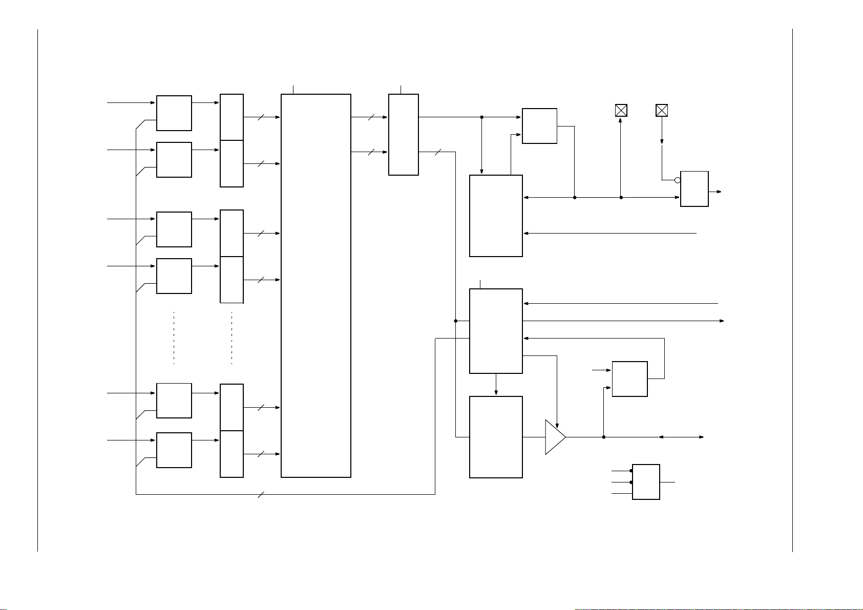
100 Micronas
VCT 38xxA ADVANCE INFORMATION
Int-Input 1
Int-Input 2
Int-Input 3
Int-Input 4
Pending
Register
R
Q
S
R
Q
S
R
Q
S
R
Q
S
Priority
Registers
IRPRI10
IRPRI32
4
prio
4
4
4
clke
Parallel
Priority
Decoder
Priority
Latch
4
priority
4 4
input #
clke
Priority
Stack
15 x 4
clke
Ctrl
A
A>B
B
push
pull
CCUNMIDISCCUNMI
&
NMI
IRRET write
DMAE
RDY
Int-Input 15
Int-Input 16
R
Q
S
R
Q
S
Clear Request
IRPRIFE
16
Fig. 5–10: Block diagram of interrupt logic
00FFFA
4
Interrupt
Vect or
4
Ta bl e
16
enable
PAT CH
DMAE
Ph2
A
A=B
B
A0...A23
&
clke
 Loading...