

Page 1
Copyright © 1998, V3 Semiconductor Inc. V960PBC Data Sheet Rev 2.4 1
V960PBC Rev. B2
LOCAL BUS TO PCI BRIDGE
FOR i960Sx PROCESSORS
V3 Semiconductor reserves the right to change the specifications of this product without notice.
V960PBC and V96SSC are trademarks of V3 Semiconductor. All other trademarks are the property of their respective owners.
• Glueless interface between Intel i960Sx,
processors and PCI bus
• Fully compliant with PCI 2.1 specification
• Configurable for primary master, bus master, or
target operation
• Up to 1Kbyte burst access support on both local
and PCI interface
• 576 bytes of programmable FIFO storage with
DYNAMIC BANDWIDTH ALLOCATION™
• Two channel DMA controller
• Enhanced support for 8/16-bit local bus devices
with programmable region size register
• 16 8-bit bi-directional mailbox registers with
doorbell interrupts
• Dual bi-directional address space remapping
• On-the-fly byte order (endian) conversion
• Optional power on serial EEPROM initialization
• I2O ATU and messaging unit including
hardware controlled circular queues
• Flexible PCI and local interrupt management
• Support for real-mode DOS "holes"
• Ability to generate both Type 0 and Type 1
configuration cycles
• 33MHz and 40MHz local bus versions available
with independent PCI operation up to 33MHz
• Low cost 160-pin EIAJ PQFP package
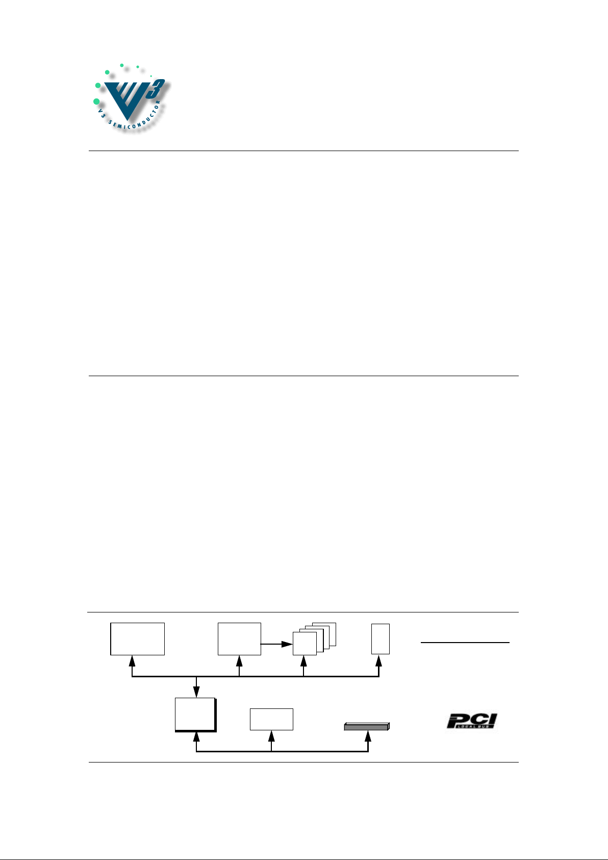
V960PBC provides the highest performance,
most flexible, and most economical method to
directly connect i960Sx processor to the PCI
bus. V961PBC may also be used in systems
without a CPU for a generic PCI master/target
interface.
V960PBC Rev B2 is the first I2O ready PCI
bridge, fully backward compatible with V960PBC
Rev B1. The PCI bus can be run at the full
33MHz frequency, independent of local bus
clock rate. The overall throughput of the system
is dramatically improved by increasing the FIFO
depth and utilizing the unique DYNAMIC
BANDWIDTH ALLOCATION™ architecture.
Access to the PCI bus can be performed through
two programmable address apertures. Two more
apertures are provided for PCI-to-local bus
accesses. There are 32-bytes of read FIFO’s in
each direction, 16-byte dedicated for each
aperture.
V960PBC also includes bi-directional remapping
capabilities, and on-the-fly byte order conversion
Two DMA channels are provided for autonomous
PCI-to-Local/Local-to-PCI transfers. Mailbox
registers and flexible PCI interrupt controllers are
also included to provide a simple mechanism to
emulate PCI device control ports.
The part is available in 160-pin low cost EIAJ
Plastic Quad Flat Pack (PQFP) package.
i960Sx
CPU
V96SSC
MEMORY
CONTROL
D
R
A
M
ROM
V960PBC
LOCAL TO
PCI BRIDGE
TYPICAL APPLICATION
PERIPHERAL
PCI
PCI SLOT or EDGE CONNECTOR
Page 2
V960PBC
2 V960PBC Data Sheet Rev 2.4 Copyright © 1998, V3 Semiconductor Inc.
This document contains the product codes, pinouts, package mechanical information, DC
characteristics, and AC characteristics for the V960PBC. Detailed functional information is contained
in the User’s Manual.
V3 Semiconductor retains the rights to change documentation, specifications, or device
functionality at any time without notice. Please verify that you have the latest copy of all
documents before finalizing a design.
1.0 Product Codes
2.0 Pin Description and Pinout
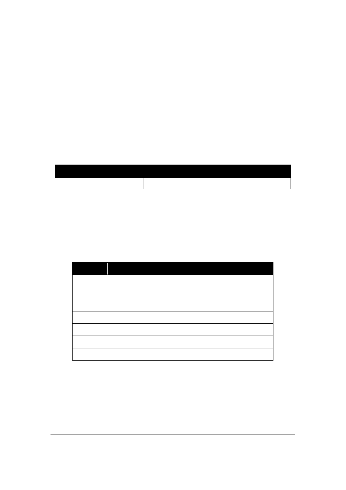
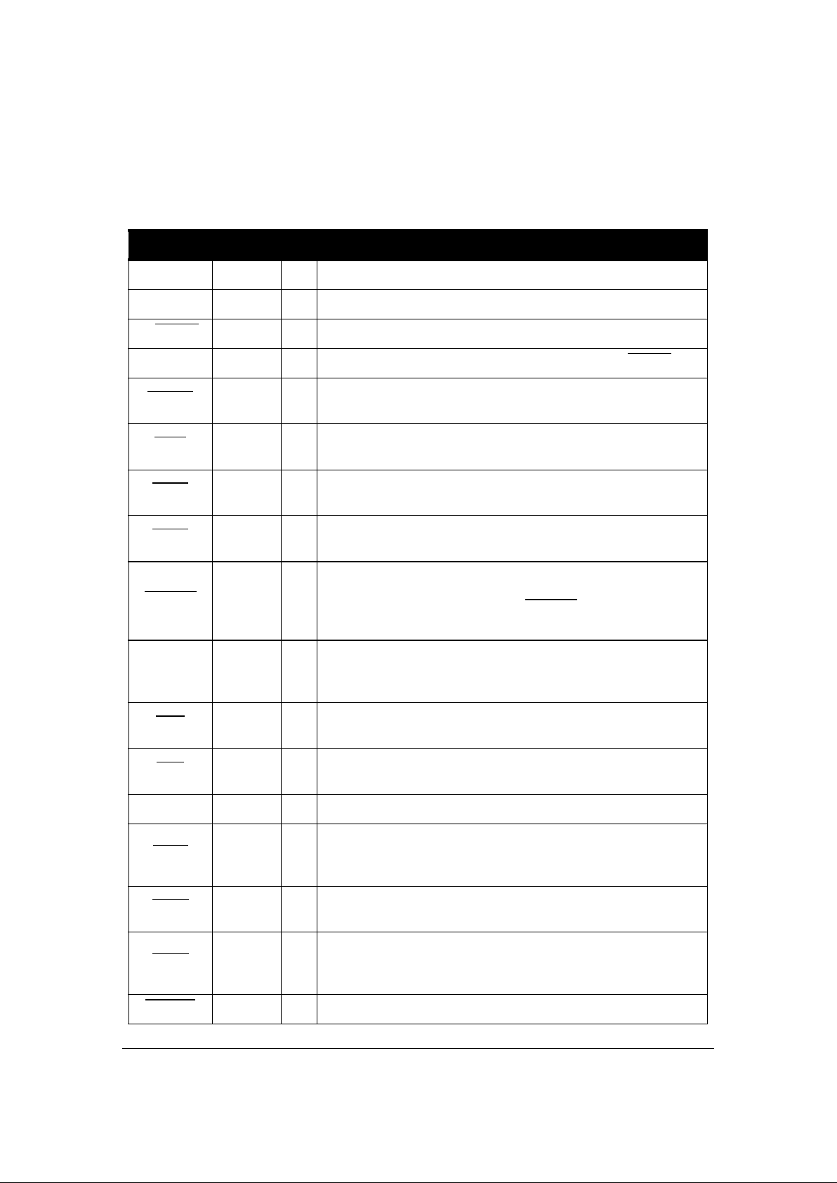
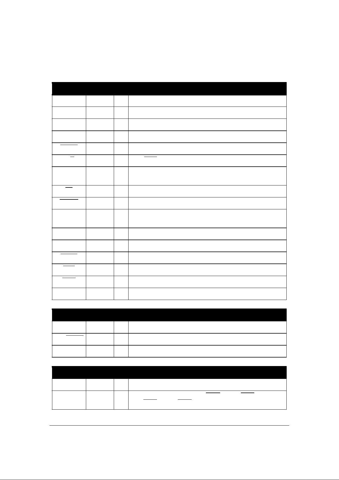
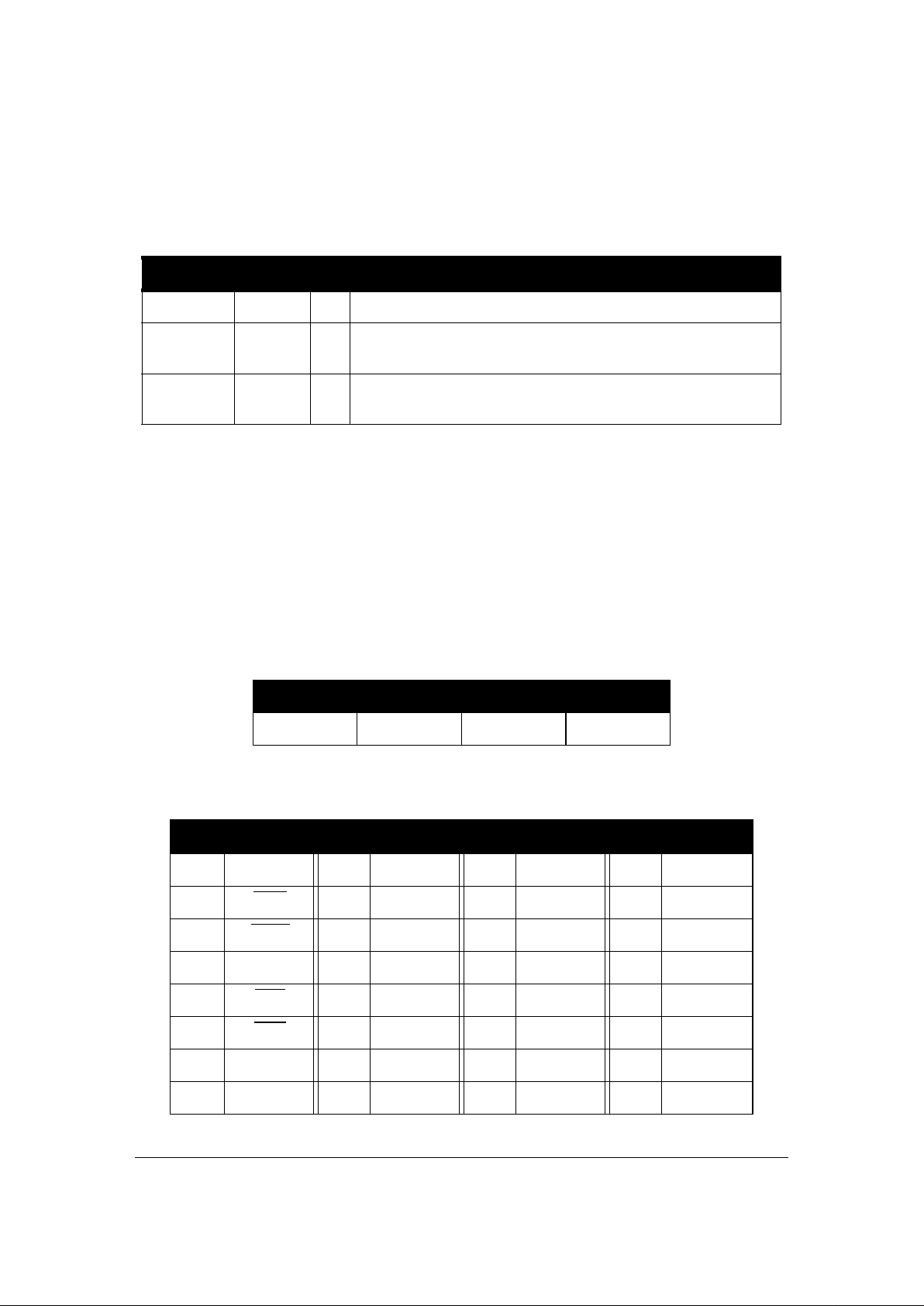
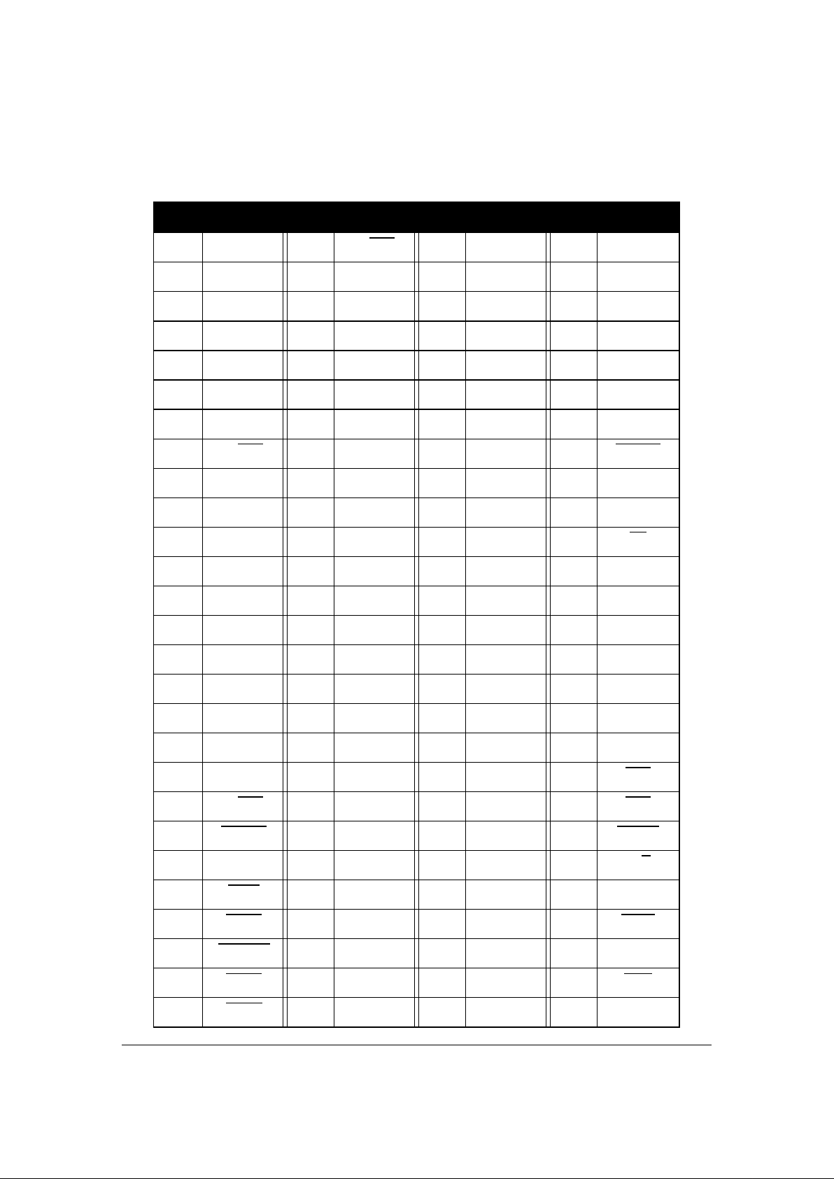
Table 2 below lists the pin types found on the V960PBC. Table 3 describes the function of each pin on
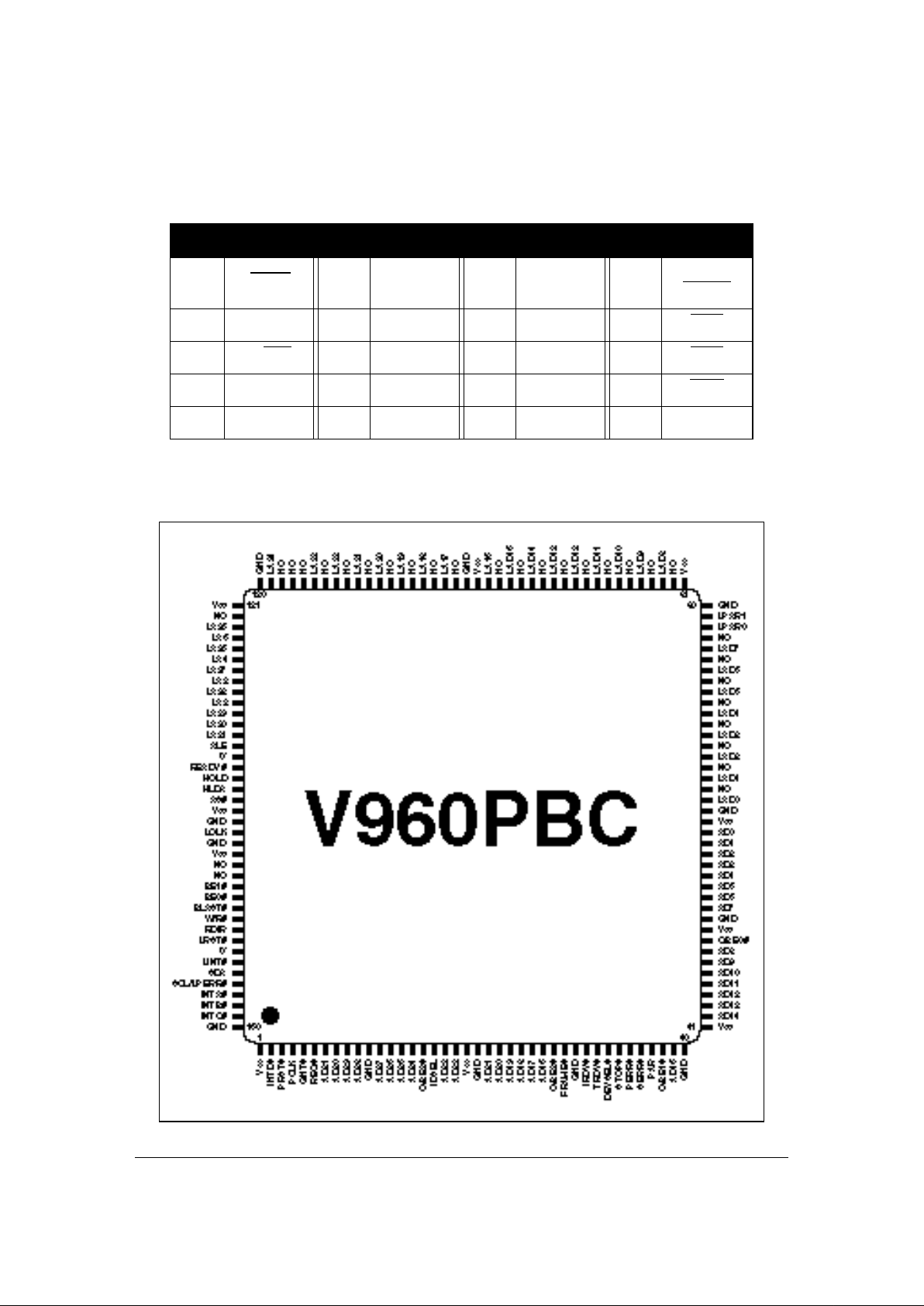
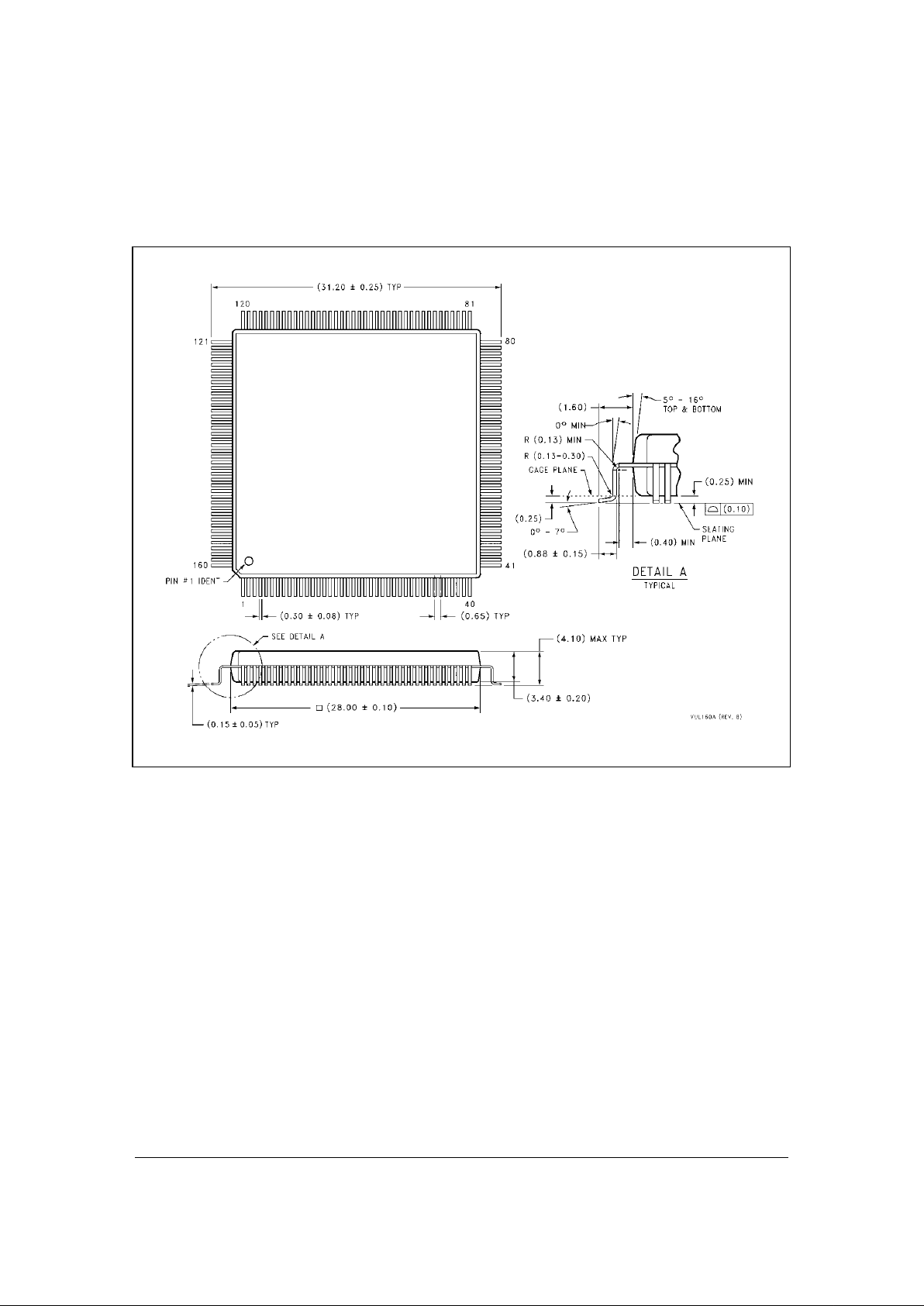
the V960PBC. Table 5 lists the pins by pin number. Figure 1 shows the pinout for the 160-pin EIAJ
PQFP package and Figure 2 shows the mechanical dimensions of the package.
Table 1: Product Codes
Product Code Processor Bus Type Package Frequency
V960PBC-33 REV B2 i960SA/SB 16-bit multiplexed 160-pin EIAJ PQFP 33MHz
Table 2: Pin Types
Pin Type Description
PCI I PCI input only pin.
PCI O PCI output only pin.
PCI I/O PCI tri-state I/O pin.
PCI I/OD PCI input with open drain output.
I/O
4
TTL I/O pin with 4mA output drive.
I TTL input only pin.
O
4
TTL output pin with 4mA output drive.
Page 3
V960PBC
Copyright © 1998, V3 Semiconductor Inc. V960PBC Data Sheet Rev 2.4 3
Table 3: Signal Descriptions
PCI Bus Interface
Signal Type R
a
Description
AD[31:0] PCI I/O Z Address and data, multiplexed on the same pins.
C/BE[3:0] PCI I/O Z Bus Command and Byte Enables, multiplexed on the same pins.
PAR PCI I/O Z Parity represents even parity across AD[31:0] and C/BE[3:0].
FRAME PCI I/O Z
Cycle Frame indicates the beginning and burst length of an
access.
IRDY PCI I/O Z
Initiator Ready indicates the initiating agent’s (bus master’s) ability
to complete the current data phase of the transaction.
TRDY PCI I/O Z
Target Ready indicates the target agent’s (selected device’s) ability to complete the current data phase of the transaction.
STOP PCI I/O Z
Stop indicates the current target is requesting the master to stop
the current transaction (retry or disconnect).
DEVSEL PCI I/O Z
Device Select, when actively driven by a target, indicates the driving device has decoded its address as the target of the current
access. As an input to the initiator, DEVSEL indicates whether
any device on the bus has been selected.
IDSEL PCI I
Initialization Device Select is used as a chip select during configuration read and write transactions. It must be driven high in order
to access the chip’s internal configuration space.
REQ PCI O H
Request indicates to the arbiter that this agent requests use of the
bus.
GNT PCI I
Grant indicates to the agent that access to the bus has been
granted.
PCLK PCI I PCLK provides timing for all transactions on the PCI bus.
PRST PCI I/O Z/L
Acts as an input when RDIR is high, an output when RDIR is low.
As an input it is asserted low to bring all internal PBC operation to
a reset state.
PERR PCI I/O Z
Parity Error is used to report data parity errors during all PCI
transactions except a Special Cycle.
SERR PCI I/OD Z
System Error is used to report address parity errors, data parity
errors on the Special Cycle command, or any other system error
where the result will be catastrophic.
INT[A:D] PCI I/OD Z Level-sensitive interrupt requests may be received or generated.
Page 4
V960PBC
4 V960PBC Data Sheet Rev 2.4 Copyright © 1998, V3 Semiconductor Inc.
Local Bus Interface
Signal Type R Description
LA[31:16] I/O4 Z Local address bus.
LAD[15:0] I/O4 Z Local multiplexed address and data bus.
LA[5:2] I/O4 Z Local address bus.
BE[1:0] I/O4 Z Local bus byte enables.
W/R I/O4 Z Write/Read.
ALE I/O4 Z
Address Latch Enable: used to latch the address during the
address phase.
AS I/O4 Z Asserted low to indicate the beginning of a bus cycle.
READY I/O4 Z Local Bus data ready.
HOLD O4 L
Local bus hold request: asserted by the chip to initiate a local bus
master cycle.
HLDA I Local bus hold acknowledge.
LPAR[1:0] I/O4 Z Local bus parity.
BLAST I/O4 Z Burst last.
LINT O4 H Local interrupt request.
LRST I/O4 L/Z Local bus RESET signal.
LCLK I Local bus clock.
Serial EEPROM Interface
Signal Type R Description
SCL/LPERR O4 X EEPROM clock. Local parity error.
SDA I/O4 X EEPROM data.
Configuration
Signal Type R Description
RDIR I
Reset direction. Tie low to drive PRST out and LRST in, high to
drive LRST out and PRST in.
Table 3: Signal Descriptions (cont’d)
Page 5
V960PBC
Copyright © 1998, V3 Semiconductor Inc. V960PBC Data Sheet Rev 2.4 5
2.1 Test Mode Pins
Several device pins are used during manufacturing test to put the V960PBC device into various test
modes. These pins must be maintained at proper levels during reset to insure proper operation.
This is typically handled through pull-up or pull-down resistors (typically 1K to 10K) on the signal pins if
they are not guaranteed to be at the proper level during reset. Table 4 below shows the reset states for
test mode pins:
Power and Ground Signals
Signal Type R Description
V
CC
-
POWER leads intended for external connection to a VCC board
plane.
GND -
GROUND leads intended for external connection to a GND board
plane.
a. R indicates state during reset.
Table 4: RESET State for Test Mode Pins
PIN# 134 135 153
Connection Pull-Down Pull-Down Pull-Down
Table 5: Pin Assignments
PIN # Signal PIN # Signal PIN # Signal PIN # Signal
1 V
CC
41 V
CC
81 V
CC
121 V
CC
2 INTD 42 AD14 82 NC 122 NC
3 PRST 43 AD13 83 LAD8 123 LA25
4 PCLK 44 AD12 84 NC 124 LA5
5 GNT 45 AD11 85 LAD9 125 LA26
6 REQ 46 AD10 86 NC 126 LA4
7 AD31 47 AD9 87 LAD10 127 LA27
8 AD30 48 AD8 88 NC 128 LA3
Table 3: Signal Descriptions (cont’d)
Page 6
V960PBC
6 V960PBC Data Sheet Rev 2.4 Copyright © 1998, V3 Semiconductor Inc.
9 AD29 49 C/BE0 89 LAD11 129 LA28
10 AD28 50 V
CC
90 NC 130 LA2
11 GND 51 GND 91 LAD12 131 LA29
12 AD27 52 AD7 92 NC 132 LA30
13 AD26 53 AD6 93 LAD13 133 LA31
14 AD25 54 AD5 94 NC 134 ALE
15 AD24 55 AD4 95 LAD14 135 '0'
16 C/BE3 56 AD3 96 NC 136 READY
17 IDSEL 57 AD2 97 LAD15 137 HOLD
18 AD23 58 AD1 98 NC 138 HLDA
19 AD22 59 AD0 99 LA16 139 AS
20 V
CC
60 V
CC
100 V
CC
140 V
CC
21 GND 61 GND 101 GND 141 GND
22 AD21 62 LAD0 102 NC 142 LCLK
23 AD20 63 NC 103 LA17 143 GND
24 AD19 64 LAD1 104 NC 144 V
CC
25 AD18 65 NC 105 LA18 145 LA1
26 AD17 66 LAD2 106 NC 146 NC
27 AD16 67 NC 107 LA19 147 BE1
28 C/BE2 68 LAD3 108 NC 148 BE0
29 FRAME 69 NC 109 LA20 149 BLAST
30 GND 70 LAD4 110 NC 150 W/R
31 IRDY 71 NC 111 LA21 151 RDIR
32 TRDY 72 LAD5 112 NC 152 LRST
33 DEVSEL 73 NC 113 LA22 153 ’0’
34 STOP 74 LAD6 114 NC 154 LINT
35 PERR 75 NC 115 LA23 155 SDA
Table 5: Pin Assignments (cont’d)
PIN # Signal PIN # Signal PIN # Signal PIN # Signal
Page 7
V960PBC
Copyright © 1998, V3 Semiconductor Inc. V960PBC Data Sheet Rev 2.4 7
Figure 1: Pinout for 160-pin EIAJ PQFP (top view)
36 SERR 76 LAD7 116 NC 156
SCL/
LPERR
37 PAR 77 NC 117 NC 157 INTA
38 C/BE1 78 LPAR0 118 NC 158 INTB
39 AD15 79 LPAR1 119 LA24 159 INTC
40 GND 80 GND 120 GND 160 GND
Table 5: Pin Assignments (cont’d)
PIN # Signal PIN # Signal PIN # Signal PIN # Signal
Page 8
V960PBC
8 V960PBC Data Sheet Rev 2.4 Copyright © 1998, V3 Semiconductor Inc.
Figure 2: 160-pin EIAJ PQFP mechanical details
Unit of Measurement = millimeters
Page 9
V960PBC
Copyright © 1998, V3 Semiconductor Inc. V960PBC Data Sheet Rev 2.4 9
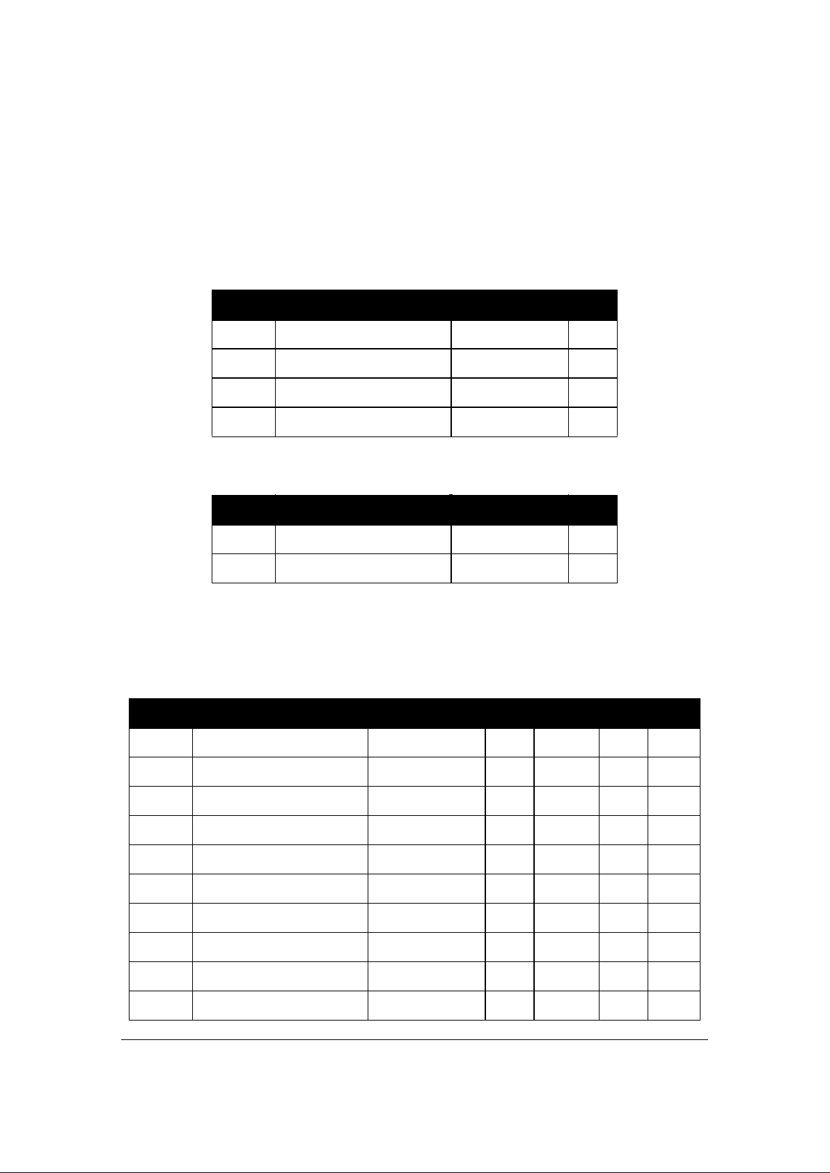
3.0 DC Specifications
The DC specifications for the PCI bus signals match exactly those given in the PCI Specification, Rev.
2.1, Section 4.2.1.1. For more information on the PCI DC specifications, see the PCI Specification.
3.1 PCI Bus DC Specifications
Table 6: Absolute Maximum Ratings
Symbol Parameter Value Units
V
CC
Supply voltage -0.3 to +7 V
V
IN
DC input voltage -0.3 to VCC+0.3 V
I
IN
DC input current ± 10 mA
T
STG
Storage temperature range -40 to +125 °C
Table 7: Guaranteed Operating Conditions
Symbol Parameter Value Units
V
CC
Supply voltage 4.75 to 5.25 V
T
A
Ambient temperature range 0 to 70 °C
Table 8: PCI Bus Signals DC Operating Specifications
Symbol Parameter Condition Min Max Units Notes
V
IH
Input high voltage 2.0 VCC+0.5 V
V
IL
Input low voltage -0.5 0.8 V
I
IH
Input high leakage current VIN = 2.7V 70 µA 1
I
IL
Input low leakage current VIN = 0.5V -70 µA 1
V
OH
Output high voltage I
OUT
= -2mA 2.4 V
V
OL
Output low voltage I
OUT
= 3mA, 6mA 0.55 V 2
C
IN
Input pin capacitance 10 pF 3
C
CLK
PCLK pin capacitance 5 12 pF
C
IDSEL
IDSEL pin capacitance 8 pF 4
L
PIN
Pin inductance 20 nH
Page 10
V960PBC
10 V960PBC Data Sheet Rev 2.4 Copyright © 1998, V3 Semiconductor Inc.
Notes:
1. Input leakage currents include high impedance output leakage for all bi-directional buffers with tri-state outputs.
2. Signals without pull-up resistors have greater than 3mA low output current. Signals requiring pull resistors
have greater than 6mA output current. The latter include FRAME, TRDY, IRDY, STOP, SERR, PERR.
3. Absolute maximum pin capacitance for a PCI unit is 10pF (except for CLK).
4. Lower capacitance on this input-only pin allows for non-resistive coupling to AD[xx].
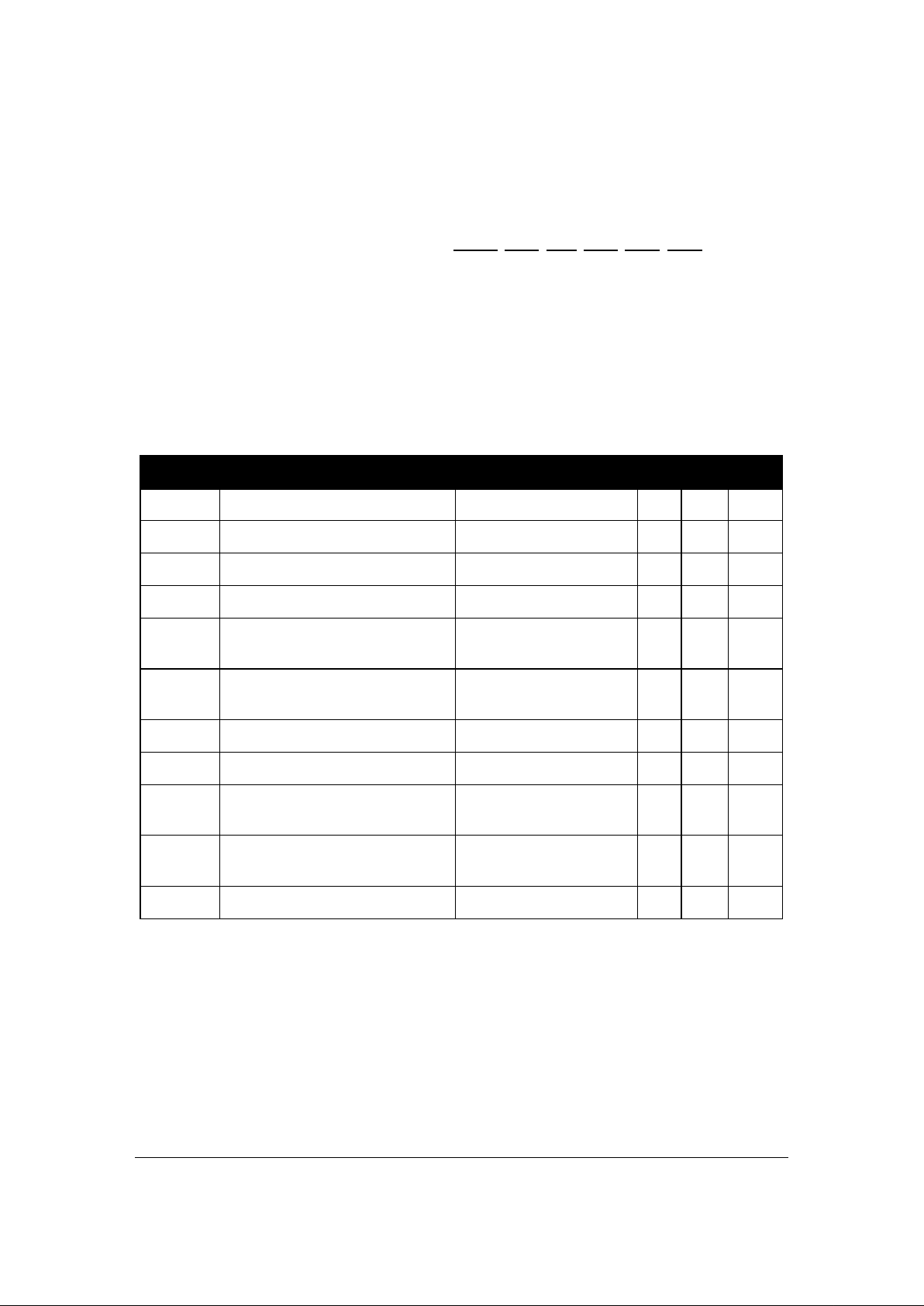
3.2 Local Bus DC Specifications
Table 9: Local Bus Signals DC Operating Specifications
Symbol Description Conditions Min Max Units
V
IL
Low level input voltage VCC = 4.75V 0.8 V
V
IH
High level input voltage VCC = 5.25V 2.0 V
I
IL
Low level input current VIN=GND, VCC=5.25V -10 µA
I
IH
High level input current V
IN
= V
CC
= 5.25V 10 µA
V
OL4
Low level output voltage for 4 mA
outputs and I/O pins
I
OL
= -4 mA 0.4 V
V
OH4
High level output voltage for 4 mA
outputs and I/O pins
I
OH
= 4 mA 2.4 V
I
OZL
Low level float input leakage V
IN
= GND -10 µA
I
OZH
High level float input leakage V
IN
= V
CC
10 µA
ICC (max) Maximum supply current
V
CC
= 5.25V
PCLK = LCLK = 33MHz
150 mA
I
CC
(typ) Typical supply current
V
CC
= 5.0V
PCLK = LCLK = 33MHz
120 mA
C
IO
Input and output capacitance 10 pF
Page 11
V960PBC
Copyright © 1998, V3 Semiconductor Inc. V960PBC Data Sheet Rev 2.4 11
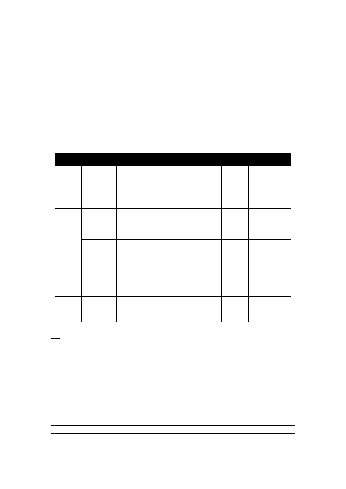
4.0 AC Specifications
The AC specifications for the PCI bus signals match exactly those given in the PCI Specification, Rev.
2.1, Section 4.2.1.2. For more information on the PCI AC specifications, including the V/I curves for 5V
signalling, see section 4.2.1.2 of Rev 2.1 PCI Specification.
4.1 PCI Bus Timings
Notes:
1. Refer to the V/I curves in Section 4.2.1 of the PCI Specification. This specification does not apply to CLK and
RST which are system outputs. “Switching Current High” specifications are not relevant to open drain outputs
such as SERR and INTA-INTD.
2. Note that this segment of the minimum current curve is drawn from the AC drive point directly to the DC drive
point rather than toward the voltage rail (as it does in the pull-down curve). This difference is intended to allow
for an optional N-channel pull-up.
3. Maximum current requirements are met as drivers pull beyond the first step voltage (AC drive point). Equations
defining these maximums (A and B) are provided with the respective V/I curves given in the PCI Spec. The equation defined maxima is met by design.
4. The minimum slew rate (slowest signal edge) is met by the PCI drivers. The maximum slew rate (fastest signal
edge) is a guideline. Motherboard designers must bear in mind that rise and fall times faster than this maximum
guideline could occur, and should ensure that signal integrity modeling accounts for this.
Table 10: PCI Bus Signals AC Operating Specifications
Symbol Parameter Condition Min Max Units Notes
I
OH(AC)
Switching
current high
0V<V
OUT
≤1.4V -44 mA 1
1.4V<V
OUT
<2.4V -44+(V
OUT
-1.4)/0.024
Equation
A
mA 1, 2, 3
(Test point) V
OUT
=3.1V -142 mA 3
I
OL(AC)
Switching
current low
V
OUT
≥2.2V 95 mA 1
2.2V>V
OUT
>0.55 V
OUT
/0.023
Equation
B
mA 1, 3
(Test point) V
OUT
=0.71 206 mA 3
I
CL
Low clamp
current
-5<VIN≤-1 -25+(VIN+1)/0.015 mA
t
R
Unloaded
output rise
time
0.4V to 2.4V 1 5 V/ns 4
t
F
Unloaded
output fall
time
2.4V to 0.4V 1 5 V/ns 4
Equation A: IOH = 11.9·(V
OUT
- 5.25V)·(V
OUT
+ 2.45V) for VCC > V
OUT
> 3.1V
Equation B: IOL = 78.5·V
OUT
(4.4V - V
OUT
) for 0V < V
OUT
< 0.71V
Page 12
V960PBC
12 V960PBC Data Sheet Rev 2.4 Copyright © 1998, V3 Semiconductor Inc.
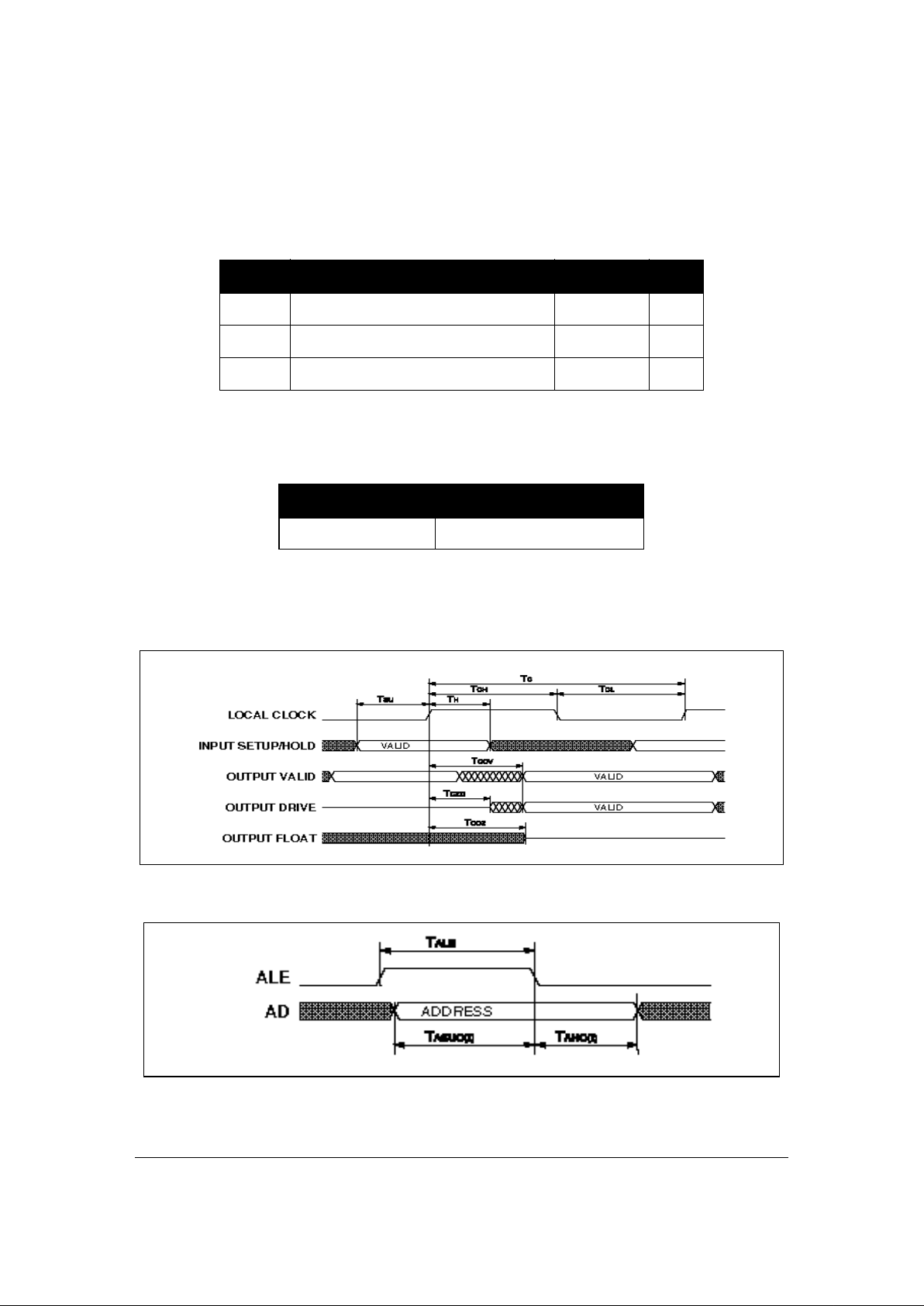
4.2 Local Bus Timings
Figure 3: Clock and Synchronous Signals
Figure 4: ALE Signal
Table 11: i960Sx Local Bus AC Test Conditions
Symbol Parameter Limits Units
V
CC
Supply voltage 4.75 to 5.25 V
V
IN
Input low and high voltages 0.4 and 2.0 V
C
OUT
Capacitive load on output and I/O pins 50 pF
Table 12: Capacitive Derating for Output and I/O Pins
Output Drive Limit Derating
4mA 0.058 ns/pF for loads > 50pF
Page 13
V960PBC
Copyright © 1998, V3 Semiconductor Inc. V960PBC Data Sheet Rev 2.4 13
Notes:
1. Measured at 1.5V.
2. All local bus signals except those in 4a, 4b, 4c, 4d and 4e.
3. All local bus signals except those in 6a.
4. READY, BLAST, AS are driven to high impedance at the falling edge of LCLK.
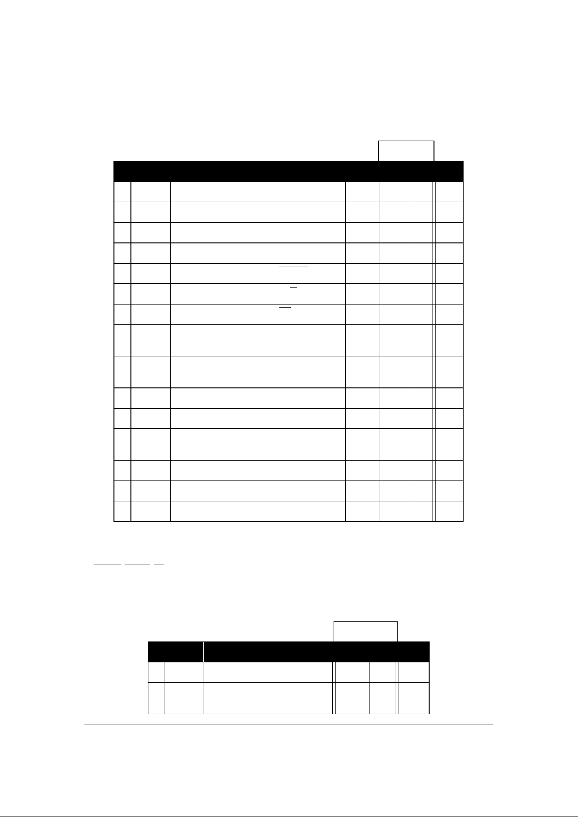
Table 13: Local Bus Timing Parameters for Vcc = 5 Volts +/- 5%
33MHz
# Symbol Description Notes Min Max Units
1 T
C
LCLK period 30 ns
2 T
CH
LCLK high time 1 12 ns
3 T
CL
LCLK low time 1 12 ns
4 T
SU
Synchronous input setup 2 7 ns
4a T
SU
Synchronous input setup (BLAST) 8 ns
4b T
SU
Synchronous input setup (W/R) 4
4c T
SU
Synchronous input setup (AS) 6
4d T
SU
Synchronous input setup (address, data,
byte enables)
9
4e T
SU
Synchronous input setup for read data
when in local bus master mode
5
5 T
H
Synchronous input hold 2 ns
6 T
COV
LCLK to output valid delay 3 3 14 ns
6a T
COV
LCLK to output valid delay (address, data,
byte enable, parity)
3 15 ns
7 T
CZO
LCLK to output driving delay 3 15 ns
8 T
COZ
LCLK to high impedance delay 4 3 15 ns
9 T
RST
Reset period when LRST used as input 16·T
C
ns
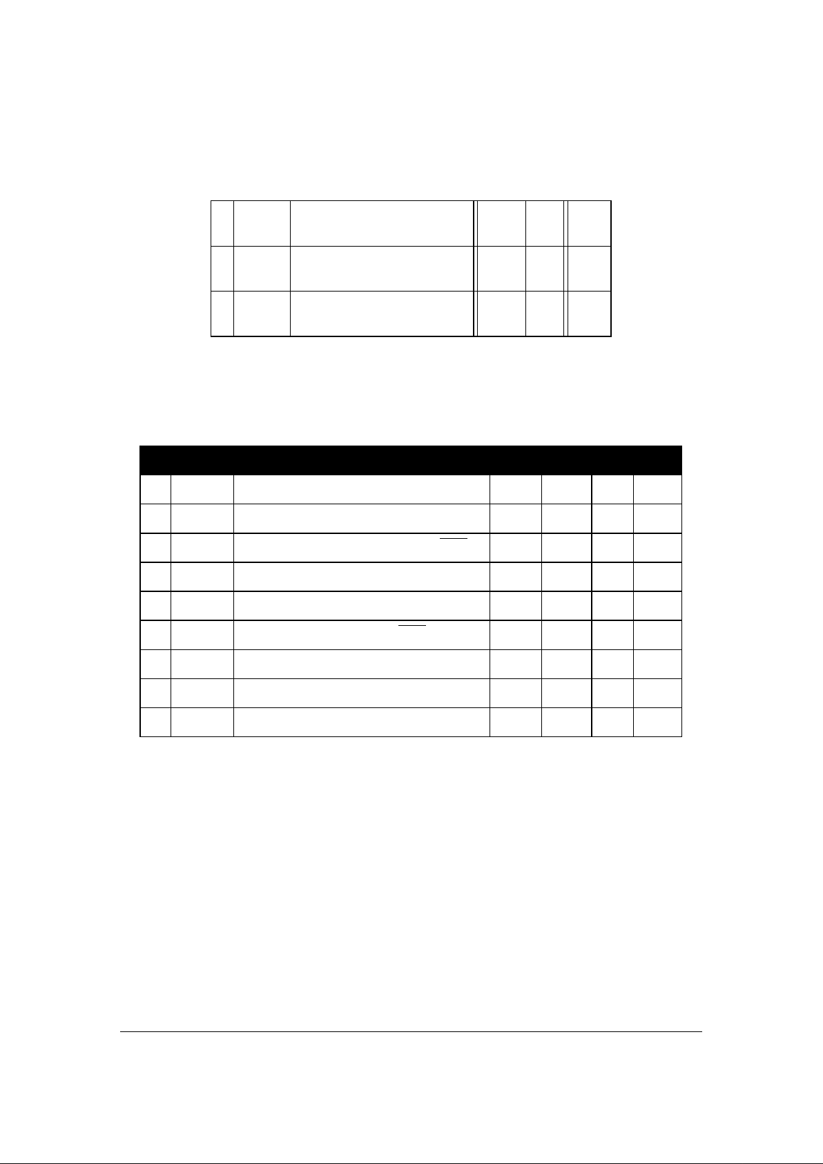
Table 14: ALE Timing Parameters for Vcc = 5 Volts +/- 5%
33MHz
# Symbol Description Min Max Units
1 T
ALE
ALE Pulse Width TCH-4 ns
2 T
ASUO
Address setup to ALE falling
(ALE as output)
TCH-5 ns
Page 14
V960PBC
14 V960PBC Data Sheet Rev 2.4 Copyright © 1998, V3 Semiconductor Inc.
Notes:
1. All PCI bus signals except those in 2a.
2. All PCI bus signals except those in 4a.
4.3 Serial EEPROM Port TImings
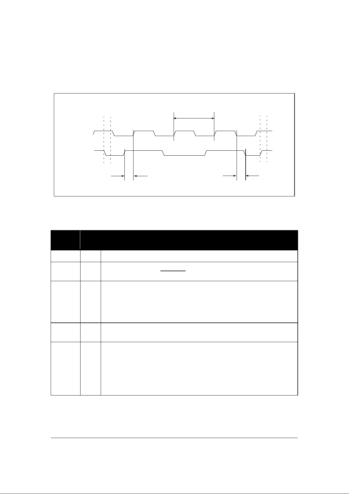
The clock for the serial EEPROM interface is derived by dividing the PCI bus clock. The waveforms
generated are shown in Figure 5.
3 T
AHO
Address hold from ALE falling
(ALE as output)
TCL-5 ns
4 T
ASUI
Address setup to ALE falling
(ALE as input)
5 ns
5 T
AHI
Address hold from ALE falling
(ALE as input)
5 ns
Table 15: PCI Bus Timing Parameters for Vcc = 5 Volts +/- 5%
# Symbol Description Notes Min Max Units
1 T
C
PCLK period 30 ns
2 T
SU
Synchronous input setup to PCLK 1 7 ns
2a T
SU
Synchronous input setup to PCLK (GNT) 10 ns
3 T
H
Synchronous input hold from PCLK 0 ns
4 T
COV
PCLK to output valid delay 2 3 11 ns
4a T
COV
PCLK to output valid delay (REQ) 4 12 ns
5 T
CZO
PCLK to output driving delay 4 11 ns
6 T
COZ
PCLK to high impedance delay 5 18 ns
7 T
RST
Reset period when PRST used as input 16·T
C
Table 14: ALE Timing Parameters for Vcc = 5 Volts +/- 5%
Page 15
V960PBC
Copyright © 1998, V3 Semiconductor Inc. V960PBC Data Sheet Rev 2.4 15
Figure 5: Serial EEPROM Waveforms and Timings
5.0 Revision History
Table 16: Revision History
Revision
Number
Date Comments and Changes
2.4 5/98 Data sheet update of B2-step values
2.3 10/96
Data Book revision.
1. In Table 3, changed “LPAR[1:0]” to “LPAR[1:0]”.
2.2 06/96
1. In Table 3, changed “PERR I/OD” to “PERR I/O”.
2. In Table 3, changed “LAD[31:0]” to “LA[31:16]”.
3. In Table 3, added “LAD[15:0]”, “VCC”, and “GND” description.
4. In Table 5, changed “LPAR2” and “LPAR3” to “NC”, “LAD24” to “LA24”.
5. In Table 13 and 14 , added min T
COV
and min T
CZO
timing.
2.1 03/96
1. Updated timings to final B1-step values.
2. Simplified data sheet format.
2.0 11/95
Removed operational description (found in User’s Manual). Device related
changes:
1. LA5, LA4, LA3, LA2 pins added to pinout for V960PBC and V961PBC.
2. Changed references to PCI 2.0 to PCI 2.1 spec level compliance.
3. Updated timings to final B0-step values.
4. Added new T
CZO
timing.
5. Added test mode pin description.
SCL
SDA
START CONDITION
STOP CONDITION
512 PCI BUS
CLOCKS
256 PCI BUS
CLOCKS
256 PCI BUS
CLOCKS
Page 16

V960PBC
16 V960PBC Data Sheet Rev 2.4 Copyright © 1998, V3 Semiconductor Inc.
 Loading...