

Datasheet V826516B04SXTG-B0, V826516B04SXTG-A1, V826516B04SXTG-B1 Datasheet (Mosel Vitelic)
Page 1
MOSEL VITELIC
1
V826516B04S
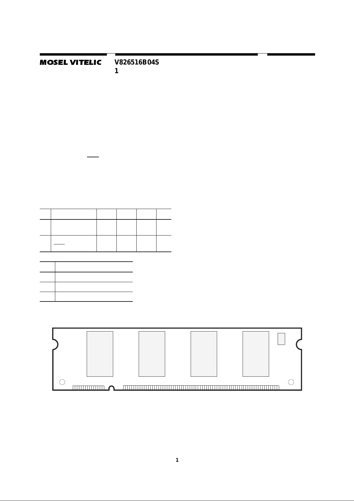
128 MB 200-PIN DDR UNBUFFERED SODIMM
2.5 VOLT 16M x 64
PRELIMINARY
V826516B04S Rev. 1.3 March 2002
Features
■ JEDEC 200 Pin DDR Unbuffered Small-Outline,
Dual In-Line memory module (SODIMM);
16,777,216 x 64 bit organization.
■ Utilizes High Performance 8M x 16 DDR
SDRAM in TSOPII-66 Packages
■ Single +2.5V (± 0.2V) Power Supply
■ Programmable CAS
Latency, Burst Length, and
Wrap Sequence (Sequential & Interleave)
■ Auto Refresh (CBR) and Self Refresh
■ All Inputs, Outputs are SSTL-2 Compatible
■ 4096 Refresh Cycles every 64 ms
■ Serial Presence Detect (SPD)
■ DDR SDRAM Performance
Description
The V826516B04S memory module is organized
16,777,216 x 64 bits in a 200 pin memory module.
The 16M x 64 memory module uses 8 Mosel-Vitelic
8M x 16 DDR SDRAM. Th e x64 modu les are ideal
for use in high performance computer systems
where increased memory den sity and fast access
times are required.
Component Used -7 -75 -8 Units
tCKClock Frequency
(max.)
143
(PC266A)
133
(PC266B)
125
(PC200)
MHz
t
AC
Cloc k Access T im e
CAS
Latenc y = 2.5
77.58ns
Module Speed
A1 PC1600 (100MHz @ CL2 )
B0 PC2100 B (133MHz @ CL2.5)
B1 PC2100 A (133MHz @ CL2)
Page 2
2
MOSEL VITELIC
V826516B04S
V826516B04S Rev. 1.3 March 2002
Part Number Information
V 8 2 65 16 B 0 4 S X T G - XX
DDRSDRAM
2.5V
WIDTH
DEPTH
200 PIN Unbuffered
SODIMM X16 COMPONENT
REFRESH
RATE 4K
4 BANKS
STTL
COMPONENT
REV LEVEL
COMPONENT
PACK AG E , T = TSOP
LEAD FINISH
G = GOLD
SPEED
A1 (100MHZ@CL2)
MOSEL VITELIC
MANUFACTURED
B0 (133MHZ@CL2.5)
B1 (133MHZ@CL2)
Page 3
MOSEL VITELIC
V826516B04S
3
V826516B04S Rev. 1.3 March 2002
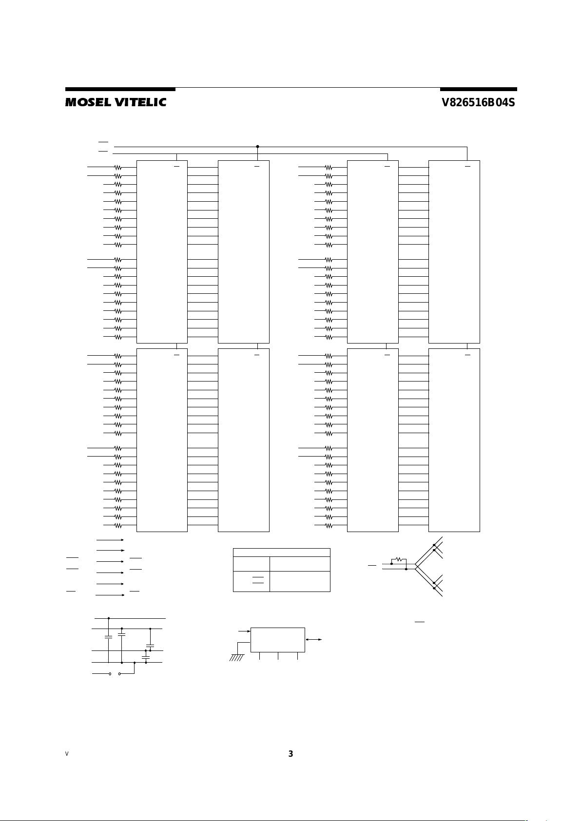
Block Diagram
S1
S0
I/0 0
I/0 1
I/0 2
I/0 3
I/0 4
I/0 5
I/0 6
I/0 7
D0
DQ0
DQ1
DQ2
DQ3
DQ4
DQ5
DQ6
DQ7
LDQS
S
S
A0 - A13
A0-A13: DDR SDRAMs D0 - D7
BA0 - BA1 BA0-BA1: DDR SDRAMs D0 - D7
RAS
RAS: SDRAMs D0 - D7
CAS
CAS: SDRAMs D0 - D7
CKE0
CKE: SDRAMs D0 - D7
WE
WE: SDRAMs D0 - D7
Notes:
1. DQ-to-I/O wiring is shown as recommended but may be changed.
2. DQ/DQS/DM/CKE/CS
relationships must
be maintained as shown.
3. DQ, DQS, DM/DQS resistors: 22 Ohms.
4. VDDID strap connections
(for memory device VDD, VDDQ):
STRAP OUT (OPEN): VDD = VDDQ
STRAP IN (VSS): VDD ≠ VDDQ.
A0
Serial PD
A1
A2
SA0 SA1
SA2
SCL
SDA
WP
V
SS
D0 - D7
D0 - D7
V
DD/VDDQ
D0 - D7
D0 - D7
VREF
V
DDID
Strap: see Note 4
V
DDSPD
SPD
Clock Wiring
Clock
Input
SDRAMs
CK0/CK0
CK1/CK1
CK2/CK2
4 SDRAMs
4 SDRAMs
NC
LDM
LDQS
LDM
DQS0
DM0
I/0 0
I/0 1
I/0 2
I/0 3
I/0 4
I/0 5
I/0 6
I/0 7
D4
I/0 8
I/0 9
I/0 10
I/0 11
I/0 12
I/0 13
I/0 14
I/0 15
DQ0
DQ1
DQ2
DQ3
DQ4
DQ5
DQ6
DQ7
UDQS
UDM
UDQS
UDM
DQS1
DM1
I/0 8
I/0 9
I/0 10
I/0 11
I/0 12
I/0 13
I/0 14
I/0 15
I/0 0
I/0 1
I/0 2
I/0 3
I/0 4
I/0 5
I/0 6
I/0 7
D2
DQ0
DQ1
DQ2
DQ3
DQ4
DQ5
DQ6
DQ7
LDQS
S
S
LDM
LDQS
LDM
DQS4
DM4
I/0 0
I/0 1
I/0 2
I/0 3
I/0 4
I/0 5
I/0 6
I/0 7
D6
I/0 8
I/0 9
I/0 10
I/0 11
I/0 12
I/0 13
I/0 14
I/0 15
DQ0
DQ1
DQ2
DQ3
DQ4
DQ5
DQ6
DQ7
UDQS
UDM
UDQS
UDM
DQS5
DM5
I/0 8
I/0 9
I/0 10
I/0 11
I/0 12
I/0 13
I/0 14
I/0 15
I/0 0
I/0 1
I/0 2
I/0 3
I/0 4
I/0 5
I/0 6
I/0 7
D1
DQ0
DQ1
DQ2
DQ3
DQ4
DQ5
DQ6
DQ7
LDQS
S
S
LDM
LDQS
LDM
DQS2
DM2
I/0 0
I/0 1
I/0 2
I/0 3
I/0 4
I/0 5
I/0 6
I/0 7
D5
I/0 8
I/0 9
I/0 10
I/0 11
I/0 12
I/0 13
I/0 14
I/0 15
DQ0
DQ1
DQ2
DQ3
DQ4
DQ5
DQ6
DQ7
UDQS
UDM
UDQS
UDM
DQS3
DM3
I/0 8
I/0 9
I/0 10
I/0 11
I/0 12
I/0 13
I/0 14
I/0 15
I/0 0
I/0 1
I/0 2
I/0 3
I/0 4
I/0 5
I/0 6
I/0 7
D3
DQ0
DQ1
DQ2
DQ3
DQ4
DQ5
DQ6
DQ7
LDQS
S
S
LDM
LDQS
LDM
DQS6
DM6
I/0 0
I/0 1
I/0 2
I/0 3
I/0 4
I/0 5
I/0 6
I/0 7
D7
I/0 8
I/0 9
I/0 10
I/0 11
I/0 12
I/0 13
I/0 14
I/0 15
DQ0
DQ1
DQ2
DQ3
DQ4
DQ5
DQ6
DQ7
UDQS
UDM
UDQS
UDM
DQS7
DM7
I/0 8
I/0 9
I/0 10
I/0 11
I/0 12
I/0 13
I/0 14
I/0 15
*Clock Net Wiring
Card
Edge
Dram1
Dram2
R=120
Ω
± 5%
CK
CK
Dram3
Dram4
Page 4
4
MOSEL VITELIC
V826516B04S
V826516B04S Rev. 1.3 March 2002
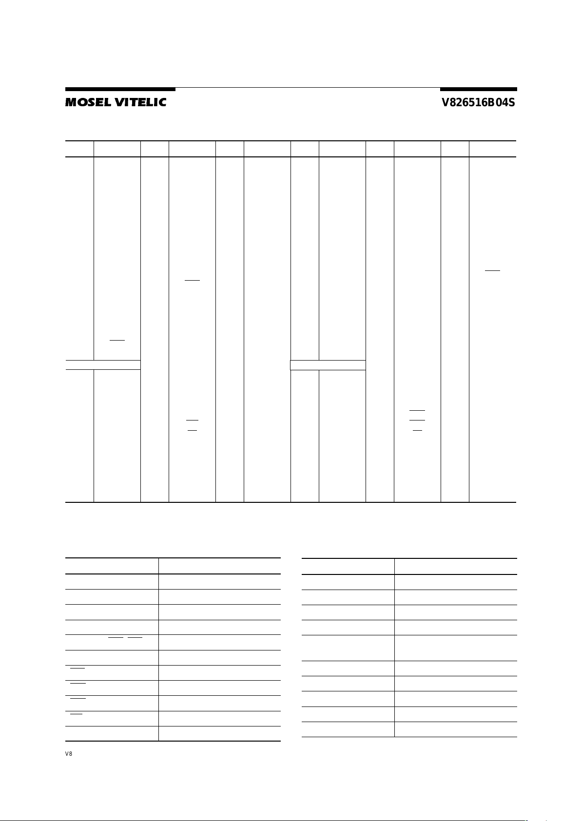
Pin Configurations (Front Side/Back Side)
Notes:
* These pins ar e not used in this module.
Pin Front Pin Front Pin Front Pin Back Pin Back Pin Back
1
3
5
7
9
11
13
15
17
19
21
23
25
27
29
31
33
35
37
39
41
43
45
47
49
51
53
55
57
59
61
63
65
VREF
VSS
DQ0
DQ1
VDD
DQS0
DQ2
VSS
DQ3
DQ8
VDD
DQ9
DQS1
VSS
DQ10
DQ11
VDD
CK0
CK0
VSS
DQ16
DQ17
VDD
DQS2
DQ18
VSS
DQ19
DQ24
VDD
DQ25
DQS3
VSS
DQ26
67
69
71
73
75
77
79
81
83
85
87
89
91
93
95
97
99
101
103
105
107
109
111
113
115
117
119
121
123
125
127
129
131
133
DQ27
VDD
CB0
CB1
VSS
DQS8
CB2
VDD
CB3
DU
VSS
CK2
CK2
VDD
CKE1
DU(A13)
A12
A9
VSS
A7
A5
A3
A1
VDD
A10/AP
BA0
WE
S0
DU
VSS
DQ32
DQ33
VDD
DQS4
135
137
139
141
143
145
147
149
151
153
155
157
159
161
163
165
167
169
171
173
175
177
179
181
183
185
187
189
191
193
195
197
199
DQ34
VSS
DQ35
DQ40
VDD
DQ41
DQS5
VSS
DQ42
DQ43
VDD
VDD
VSS
VSS
DQ48
DQ49
VDD
DQS6
DQ50
VSS
DQ51
DQ56
VDD
DQ57
DQS7
DQ58
DQ58
DQ59
VDD
SDA
SCL
VDDSPD
VDDID
2
4
6
8
10
12
14
16
18
20
22
24
26
28
30
32
34
36
38
40
42
44
46
48
50
52
54
56
58
60
62
64
66
VREF
VSS
DQ4
DQ5
VDD
DM0
DQ6
VSS
DQ7
DQ12
VDD
DQ13
DM1
VSS
DQ14
DQ15
VDD
VDD
VSS
VSS
DQ20
DQ21
VDD
DM2
DQ22
VSS
DQ23
DQ28
VDD
DQ29
DM3
VSS
DQ30
68
70
72
74
76
78
80
82
84
86
88
90
92
94
96
98
100
102
104
106
108
110
112
114
116
118
120
122
124
126
128
130
132
134
DQ31
VDD
CB4
CB5
VSS
DM8
CB6
VDD
CB7
DU/(RESET)
VSS
VSS
VDD
VDD
CKE0
DU(BA2)
A11
A8
VSS
A6
A4
A2
A0
VDD
BA1
RAS
CAS
S1
DU
VSS
DQ36
DQ37
VDD
DM4
136
138
140
142
144
146
148
150
152
154
156
158
160
162
164
166
168
170
172
174
176
178
180
182
184
186
188
190
192
194
196
198
200
DQ38
VSS
DQ39
DQ44
VDD
DQ45
DM5
VSS
DQ46
DQ47
VDD
CK1
CK1
VSS
DQ52
DQ53
VDD
DM6
DQ54
VSS
DQ55
DQ60
VDD
DQ61
DM7
VSS
DQ62
DQ63
VDD
SA0
SA1
SA2
DU
Pin Names
Pin Pin Description
A0~A11 Address Input (Multiplexed)
BA0~BA1 Bank Select Address
DQ0~DQ63 Data Input/Output
DQS0~D Q S7 Data S trobe Input/Output
CK0~CK2, CK0
~CK2, Clock Input
CKE0 Clock Enable Input
CS0
Chip Select Input
RAS Row Address Strobe
CAS
Column Address Strobe
WE
Write Enable
DM0~DM7 Data - In Mask
VDD Power Supply (2.5V)
VDDQ Power Supply for DQS(2.5V)
VSS Ground
VREF Power Supply for Reference
VDDSPD Serial EEPOM Power Supply (2.3V
to 3.6V)
SDA Serial Data I/O
SCL Serial Clock
SA0~2 Address in EEPROM
VDDID VDD Identification Flag
NC No Connection
Pin Pin Description
Key
Key
Page 5
MOSEL VITELIC
V826516B04S
5
V826516B04S Rev. 1.3 March 2002
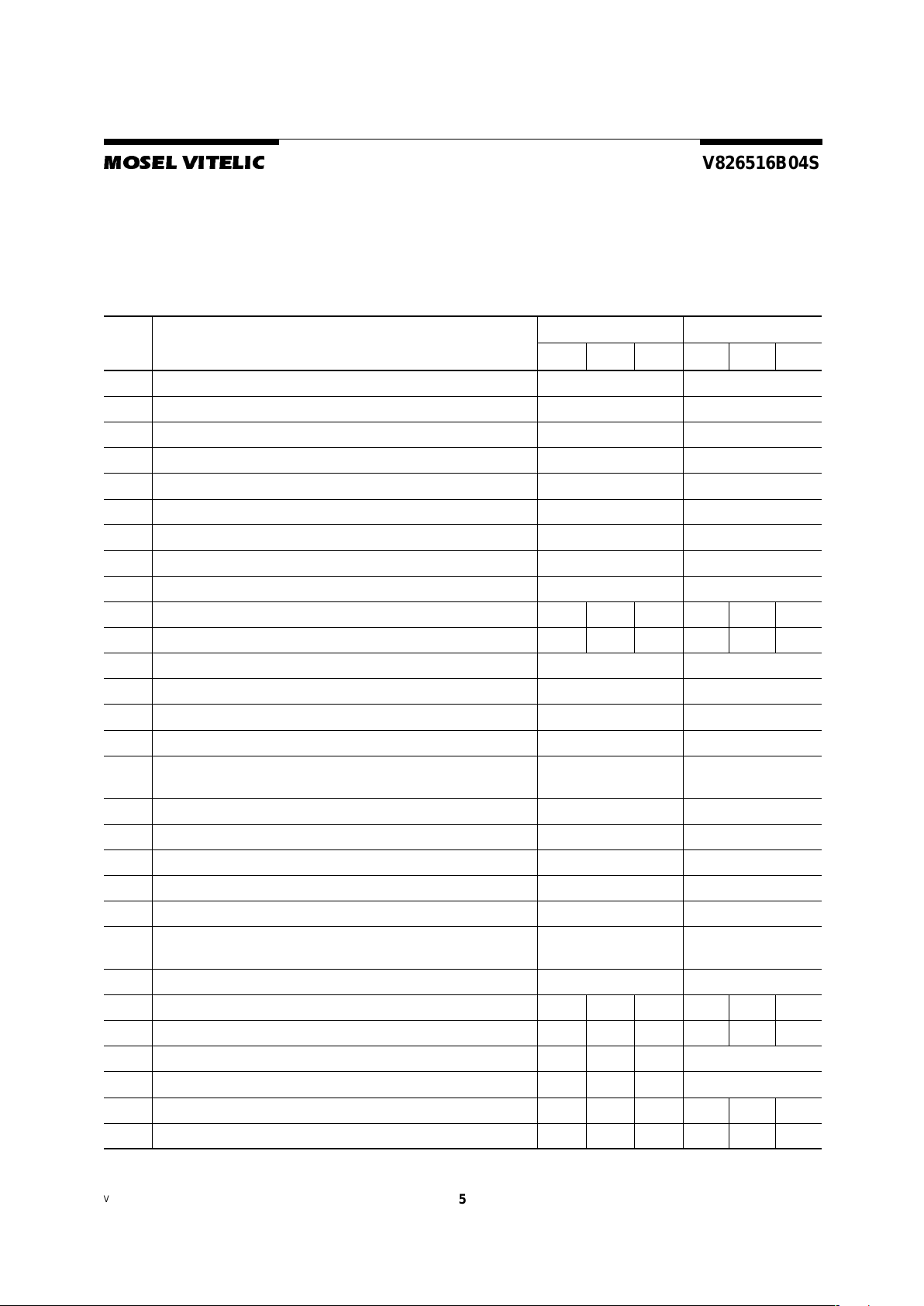
Serial Pr esence Detect Info rm ation
Bin Sort:
A1 (PC1600 @ CL2)
B0 (PC2100B @ CL2.5)
B1 (PC2100A @ CL2)
Byte # Functi on described
Function Supported Hex value
A1 B0 B1 A1 B0 B1
0 Defines # of Bytes written into serial memory at module manufacturer 128bytes 80h
1 Total # of Bytes of SPD memory device 256bytes 08h
2 Fundamental memory type SDRAM DDR 07h
3 # of row address on this assembly 12 0Ch
4 # of column address on this assembly 9 09h
5 # of module Rows on this assembly 2 Bank 02h
6 Data width of this assembly 64 bits 40h
7 .........Data width of this assembly - 00h
8 VDDQ and in terface standard of thi s as s em bly SSTL 2.5 V 04h
9 DDR SDRAM cycle time at CAS Latency =2.5 8ns 7.5ns 7ns 80h 75h 70h
10 DDR SDRAM Access time from clock at CL=2.5 ±0.8ns ±0.75ns ±0.70ns 80h 75h 70h
11 DIMM configuration type(Non-parity, Parity, ECC) Non-parity, ECC 00
12 Refresh rate & type 15.6us & Self refresh 80h
13 Primary DDR SDRAM width x16 10h
14 Error checking DDR SDRAM data width x0 00h
15 Minimum clock delay for back-to -back ra ndom column
address
t
CCD
=1CLK 01h
16 DDR SDRAM device attributes : Burst lengths supported 2,4,8 0Eh
17 DDR SDRAM device attributes : # of banks on each DDR SDRAM 4 banks 04h
18 DDR SDRAM device attributes : CAS Latency supported 2,2.5 0Ch
19 DDR SDRAM device attributes : CS Latency 0CLK 01h
20 DDR SDRAM device attributes : WE Latency 1CLK 02h
21 DDR SDRAM module attributes Unbuffered
Diff Clock
20h
22 DDR SDRAM device attributes : General +/-0.2V voltage tolerance 00h
23 DDR SDRAM cycle time at CL =2 10ns 10ns 7.5ns A0h A0h 75h
24 DDR SDRAM Access time from clock at CL =2 ±0.8ns ±0.8ns ±0.75ns 80h 80h 75h
25 DDR SDRAM cycle time at CL =1.5 - - - 00h
26 DDR SDRAM Access time from clock at CL =1.5 - - - 00h
27 Minimum row precharge time (=t
RP
) 20ns 20ns 18ns 50h 50h 48h
28 Minimu m row ac tiv a te to row ac tiv e dela y (=t
RRD
) 15ns 15ns 14ns 3Ch 3Ch 38h
Page 6

6
MOSEL VITELIC
V826516B04S
V826516B04S Rev. 1.3 March 2002
29 Minimum RAS to CAS dela y(=t
RCD
) 20ns 20ns 18ns 50h 50h 48h
30 Minimum active to precharge time(=t
RAS
) 50ns 45ns 45ns 32h 2Dh 2Dh
31 Module ROW density 64MB 10h
32 Command and address s ignal input setup time 1.1ns 0.9ns 0.9ns B0h 90h 90h
33 Command and address s ignal input hold time 1.1ns 0.9ns 0.9ns B0h 90h 90h
34 Data signal input setup time 0.6ns 0.5ns 0.5ns 60h 50h 50h
35 Data signal input hold time 0.6ns 0.5ns 0.5ns 60h 50h 50h
36-40 Superset information (may be used in future) - 00h
41 SDRAM device minimum active to active/auto-refresh time
(=t
RC
)
70ns 65ns 60ns 46H 41h 3Ch
42 SDRAM device minimum active to autorefresh to active/auto-refresh
time (=t
RFC
)
80ns 75ns 67ns 50h 4Bh 43h
43 SDRAM device maximum devi ce cycle time (=t
CK MAX
) 12ns 12ns 12ns 30h 30h 30h
44 SDRAM device maximum skew between DQS and DQ si gnals
(=t
DQSQ
)
0.6ns 0.5ns 0.5ns 3Ch 32h 32h
45 SDRAM device maximum read datahold skew factor (=t
QHS
) 1ns 0.75ns 0.75ns A0h 75h 75h
46-61 Superset information (may be used in future) - 00h
62 SPD data revision code Initial release 00h
63 Checksum for Bytes 0 ~ 62 - BC 02h A1h
64 Manufacturer JEDEC ID code Mosel Vitelic 40h
65 -71 ....... Manufacturer JEDEC ID code Mosel Vitelic 00h
72 Manufacturing location 01h
73-90 Module part number (ASCII) V826516B04S
91 Manufacturer revi son code (For PCB) 0 00
92 Manufacturer revison code (For component) 0 00
93 Manu fac tu r in g da te ( We ek ) - 94 Manu fac tu r in g da te ( Year) - -
95~98 Assembly serial # - -
99~127 Manufacturer specific data (may be used in future) Undefined 00h
128~255 Open for customer use Undefined 00h
Byte # Functi on described
Function Supported Hex value
A1 B0 B1 A1 B0 B1
Serial Pr esence Detect Info rm ation (cont . )
Page 7

MOSEL VITELIC
V826516B04S
7
V826516B04S Rev. 1.3 March 2002
DC Operating Conditions
(TA = 0 to 70°C, Voltage referenced to VSS = 0V)
Notes: 1. V
DDQ
must not exceed the level of VDD.
2. V
IL
(min) is acceptable -1.5V AC pulse width with ð 5ns of dura tion.
3. The va lue of V
REF
is approximately equal to 0.5V
DDQ
.
AC Operating Conditions
(TA = 0 to 70 °C, Voltage referenced to VSS = 0V)
Notes: 1. VID is the magnitude of the difference between the input level on CK and the input on CK.
2. The value of VIX is expected to equal 0.5*V
DDQ
of the tr ansmitting device and must track variations in the DC level of the
same.
Parameter Symbol Min Typ. Max Unit Note
Power Supply Voltage V
DD
2.3 2.5 2.7 V
Power Supply Voltage V
DDQ
2.3 2.5 2.7 V 1
Input High Voltage V
IH
V
REF
+ 0.15 - V
DDQ
+ 0.3 V
Input Low Voltage V
IL
-0.3 - V
REF
- 0.15 V 2
I/O Termination Voltage V
TT
V
REF
- 0.04 V
REF
V
REF
+ 0.04 V
Refere nce Voltage V
REF
1.15 1.25 1.35 V 3
Input Le ak ag e C urr e nt I
I
-2 - 2 µA
Output Le ak ag e C urr e nt IO
z
-5 - 5 µA
Output High Current (V
OUT
= 1.95V) IO
H
-16.8 - - mA
Output Low Current (V
OUT
= 0.35V) IO
L
16.8 - - mA
Parameter Symbol Min Max Unit Note
Input H ig h (Logic 1) Volt ag e, DQ , DQ S an d D M si gn al s V
IH(AC)
V
REF
+ 0.31 V
Input Low (Logic 0) Voltage, DQ, DQS and DM signals V
IL(AC)
V
REF
- 0.31 V
Input Differential Voltage, CK and CK
inputs V
ID(AC)
0.7 V
DDQ
+ 0.6 V 1
Input Cr os s in g P oin t Voltage, CK an d CK
inputs V
IX(AC)
0.5*V
DDQ-0.2
0.5*V
DDQ+0.2
V2
Page 8

8
MOSEL VITELIC
V826516B04S
V826516B04S Rev. 1.3 March 2002
AC Operating Test Conditions (T
A
= 0 to 70°C, Voltage referenced to VSS = 0V)
Input/Output Capacitance
(V
DD
= 2.5V, V
DDQ
= 2.5V, TA = 25°C, f = 1MHz)
Parameter Value Unit
Refere nce Voltage V
DDQ
x 0.5 V
Termination Voltage V
DDQ
x 0.5 V
AC Input High Level Voltage (V
IH
, min) V
REF
+ 0.31 V
AC Input Low Level Voltage (V
IL
, max) V
REF
- 0.31 V
Input Timing Measurement Reference Level Voltage V
REF
V
Outpu t Tim in g Measurement Ref er e nc e Le vel Voltag e V
TT
V
Input Signal maximum peak swing 1.5 V
Input minimum Signal Slew Rate 1 V/ns
Termination Resistor (R
T
) 50 ¾
Series Resistor (R
S
) 25 ¾
Output Load Capacitance for Access Time Measurement (C
L
) 30 pF
Parameter Symbol Min Max Unit
Input ca pacitance (A0 ~ A11, BA0 ~ BA1, RAS, CAS, WE) CIN1 36 45 pF
Input ca pacitance (CKE
0
) CIN
2
36 45 pF
Input ca pacitance (CS
0
) CIN
3
34 42 pF
Input ca pacitanc e ( C LK
1
, CLK2) CIN
4
34 38 pF
Data & DQS input/output capacitance (DQ
0
~DQ63) C
OUT
89pF
Input capacitance (DM 0~DM8) CIN
5
89pF
Output Load Circuit (SSTL_2)
O
utput
Z0=50Ω
C
LOAD=30pF
V
REF
=0.5*VDD
Q
RT=50Ω
Vtt=0.5*VDDQ
Page 9

MOSEL VITELIC
V826516B04S
9
V826516B04S Rev. 1.3 March 2002
DDR SDRAM IDD SPEC TABLE
* Module IDD was calcul at e d on th e ba si s of component IDD and can be differentl y me as u r ed acc ording to DQ load in g cap.
Detailed test conditions for DDR SDRAM IDD1 & IDD
IDD1 : Operating current: One bank operation
1. Typical Case : Vdd = 2.5V, T=25’ C
2. Worst Case : Vdd = 2.7V, T= 10’ C
3. Only one bank is accessed with tRC(min), Burst Mode, Address and Control inputs on NOP edge are changing once
per clock cycle. lout = 0mA
4. Timing patterns
- DDR200(100Mhz, CL=2) : tCK = 10ns, CL2, BL=4, tRCD = 2*tCK, tRA S = 5*tCK
Read : A0 N R0 N N P0 N A0 N - repeat the same timing with random addres s changing
*50% of data changing at ever y burst
- DDR266B(133Mhz, CL=2.5) : tCK = 7.5ns, CL=2.5, BL=4, t RCD = 3*tCK, tRC = 9*tCK, tRAS = 5*tCK
Read : A0 N N R0 N P0 N N N A0 N - repeat the same timing with random address changing
*50% of data changing at ever y burst
- DDR266A (133Mhz, CL=2) : tCK = 7.5ns, CL=2, BL=4, tRCD = 3*tCK, tRC = 9*tCK, tRAS = 5*tCK
Read : A0 N N R0 N P0 N N N A0 N - repeat the same timing with random address changing
*50% of data changing at ever y burst
Legend : A=Activate, R=Read, W=Write, P=Precharge, N=NOP
Symbol
B1(DDR266@CL=2) B0(DDR266@CL=2.5) A1(DDR200@CL=2)
Unit Notes
Typical Worst Typical Worst Typical Worst
IDD0 630 690 630 690 550 590 mA
IDD1 720 810 720 810 650 730 mA
IDD2P 330 350 330 350 270 290 mA
IDD2F 430 470 430 470 370 390 mA
IDD2Q 390 410 390 410 330 350 mA
IDD3P 370 390 370 390 310 330 mA
IDD3N 450 490 450 490 370 410 mA
IDD4R 950 1070 950 1070 790 930 mA
IDD4W 990 1130 990 1130 830 990 mA
IDD5 990 1090 990 1090 910 990 mA
IDD6 Normal 16 16 16 16 16 16 16
Low pow er 8 8 8 8 8 8 8 Optional
IDD7A 1610 1830 1610 1830 1310 1510 mA
Page 10

10
MOSEL VITELIC
V826516B04S
V826516B04S Rev. 1.3 March 2002
AC Characteristics (AC operating conditions unless otherwise noted)
Parameter Symbol
(PC1600) (PC2100B) (PC2100A)
Unit NoteMin Max Min Max Min Max
Row Cycle Time tRC 60 - 65 - 70 - ns
Auto Refresh Row Cycle Time t
RFC
67 - 75 - 80 - ns
Row Active Time t
RAS
45 120K 48 120K 50 120K ns
Row Address to Column Address Delay t
RCD
18 - 20 - 20 - ns
Row Active to Row Active Delay t
RRD
14 - 15 - 15 - ns
Column Address to Column Address Delay t
CCD
1 - 1 - 1 - CLK
Row Precharge Time t
RP
18 - 20 - 20 - ns
Write Recovery Time t
WR
15 - 15 - 15 - ns
Last Dat a-In to Read Command t
DRL
1 - 1 - 1 - CLK
Auto Precharge Write Recovery + Precharge Time t
DAL
35 - 35 - 35 - ns
System Clock Cycle Time CAS
Latency = 2.5 t
CK
7 12 7.5 12 8 15 ns
CAS
Latency = 2 7.5 12 10 12 10 15 ns
Clock High Level Width t
CH
0.45 0.55 0.45 0.55 0.45 0.55 CLK
Clock Low Level Width t
CL
0.45 0.55 0.45 0.55 0.45 0.55 CLK
Data-Out edge to Clock edge Skew t
AC
-0.75 0.75 -0.75 0.75 -0.8 0.8 ns
DQS-Out edge to Clock edge Skew t
DQSCK
-0.75 0.75 -0.75 0.75 -0.8 0.8 ns
DQS-Out edge to Data-Out edge Skew t
DQSQ
- 0.5 - 0.5 - 0.6 ns
Data-Out hold time from DQS t
QH
t
HPmin
-0.75ns
- t
HPmin
-0.75ns
- t
HPmin
-0.75ns
- ns 1
Clock Half Period t
HP
t
CH/L
min
- t
CH/L
min
- t
CH/L
min
- ns 1
Input Setup Time (fast slew rate) t
IS
0.9 - 0.9 - 1.1 - ns 2,3,5,6
Input Hold Time (fast slew rate) t
IH
0.9 - 0.9 - 1.1 - ns 2,3,5,6
Input Setup Time (slow sl ew rate) t
IS
1.0 - 1.0 - 1.1 - ns 2,4,5,6
Input Hold Time (slow slew rate) t
IH
1.0 - 1.0 - 1.1 - ns 2,4,5,6
Input Pulse Width t
IPW
2.2 - 2.2 - - - ns 6
Write DQS High Level Width t
DQSH
0.4 0.6 0.4 0.6 0.4 0.6 CLK
Write DQS Low Level Width t
DQSL
0.4 0.6 0.4 0.6 0.4 0.6 CLK
CLK to First Rising edge of DQS-In t
DQSS
0.75 1.25 0.75 1.25 0.75 1.25 CLK
Data-In Setup Time to DQS-In (DQ & DM) t
DS
0.5 - 0.5 - 0.6 - ns 7
Data-in Hold Time to DQS-In (DQ & DM) t
DH
0.5 - 0.5 - 0.6 - ns 7
DQ & DM Input Pulse Width t
DIPW
1.75 - 1.75 - 2 - ns
Read DQS Preamble Time t
RPRE
0.9 1.1 0.9 1.1 0.9 1.1 CLK
Read DQS Postamble Time t
RPST
0.4 0.6 0.4 0.6 0.4 0.6 CLK
Page 11

MOSEL VITELIC
V826516B04S
11
V826516B04S Rev. 1.3 March 2002
AC Characteristics (cont.)
Notes: 1. This calculation accounts for tDQSQ(max), the pulse width distortion of on-chip circuit and jitter.
2. Data sampled at the rising edges of the clock : A0~A11, BA0~BA1, CKE, CS
, RAS, CAS, WE.
3. For command/address input slew rate >=1.0V/ns
4. For command/address input slew rate >=0 .5V/ns an d <1.0V/ ns
5. CK, CK
slew rate s are >=1 .0V/ns
6. These par amet er s gua r ante e de vi ce ti mi ng , but they ar e no t nec ess ar ily te sted on e ach de vice, an d the y ma y be gua ran te ed
by design or tester correlation.
7. Data latc he d at bo t h ris in g and fallin g ed ge s of D at a S trobes(DQ S) : DQ, DM
8. Minimum of 20 0 cycl es of stabl e inp ut clo cks af ter S elf R efresh Exit c omman d, whe re CK E is he ld hi gh, is req uired to co mplete
Self Refresh Exit and lock the internal DLL circuit of DDR SDRAM.
Absolute Maximum Ratings
Note: Operation at above absolute maximum rating can adversely affect devi ce reliability
Write DQS Preamble Setup Time t
WPRES
0 - 0 - 0 - CLK
Write DQS Preamble Hold Time t
WPREH
0.25 - 0.25 - 0.25 - CLK
Write DQS Postamble Time t
WPST
0.4 0.6 0.4 0.6 0.4 0.6 CLK
Mode Register Set Delay t
MRD
2 - 2 - 2 - CLK
Power Down Exit Time t
PDEX
10 - 10 - 10 - ns
Exit Self Refresh to Non-Read Command t
XSNR
75 - 75 - 80 - ns
Exit Self Refresh to Read Command t
XSRD
200 - 200 - 200 - CLK 8
Average Perio dic Refr esh Interval t
REFI
- 15.6 - 15.6 - 15.6 us
Parameter Symbol Rating Unit
Ambient Temperature TA 0 ~ 70 °C
Storag e Temperature T
STG
-55 ~ 125 °C
Voltage on Any Pin relative to V
SS
VIN, V
OUT
-0.5 ~ 3.6 V
Voltag e on V
DD
rela tive to V
SS
V
DD
-0.5 ~ 3.6 V
Voltag e on V
DDQ
relative to V
SS
V
DDQ
-0.5 ~ 3.6 V
Output Short Circuit Current I
OS
50 mA
Power Dissipation P
D
8 W
Solderi ng Temperature • Time T
SOLDER
260 • 10 °C • Sec
Parameter Symbol
(PC1600) (PC2100B) (PC2100A)
Unit NoteMin Max Min Max Min Max
Page 12

12
MOSEL VITELIC
V826516B04S
V826516B04S Rev. 1.3 March 2002
Package Dimensions
Tolerances : ±.006(.15) unless otherwise specified
2.70
2.50
Units : Inches (Millimeters)
Full R 2x
0.17
(4.20)
0.456
11.40
1.896
(47.40)
0.24
(6.0)
0.086
0.79
(20.00)
2.15
(63.60)
(67.60)
Detail Z
0.16 ± 0.0039
(4.00
± 0.10)
0.04
± 0.0039
(1.00
± 0.1)
2-
φ 0.07
(1.80)
1.25
(31.75)
0.16 ± 0.039
(4.00
± 0.10)
0.096
(2.40)
0.07
(1.8)
0.150 Max
0.04
± 0.0039
(1.00
± 0.10)
0.157 Min
(4.00 Min)
(3.80 Max)
0.157 Min
(4.00 Min)
1
0.024 TYP
0.018
± 0.001
0.01
(0.25)
(0.45 ± 0.03)
(0.60 TYP)
0.102 Min
(2.55 Min)
Detail Y
2
0.098
2.45
40 42
39
41
ZY
199
200
Page 13

MOSEL VITELIC
V826516B04S
13
V826516B04S Rev. 1.3 March 2002
Label Information
CL = 2.5 (CLK)
t
RCD
= 3 (CLK)
t
RP
= 3 (CLK)
2533U
UNBUFFERED DIMM
PC2100 08
SPD Revision 0
0
V826516B04SXXX-XX 128MB CLXX
PC2100U-2533-080-A
XXXX-XXXXXXX
Assembly in Taiwan
A
Gerber file JEDEC
-- -
MOSEL VITELIC
Part Number
Module Density
D
IMM manufacture date code
Criteria of PC2100 or PC1600
CAS Latenc
y
Page 14

14
MOSEL VITELIC
V826516B04S
V826516B04S Rev. 1.3 March 2002
WORLDWIDE OFFICES
© Copyright , MOSEL VITELIC Corp.
Printedin U.S.A.
The information in t his document is subject to change without
notice.
MOSEL VITELIC makes no commitment to update or keep current the information contained in this document. No part of this
document may be copied or reproduced in any form or by any
means without the prior written consent of MOSEL-VITELIC.
MOSEL VITELIC subjects its products to normal quality contr
ol
samplingtechniques whichareintended to providean assuranc
e
of high quality products suitable for usual commercial applic
a-
tions.MOSELVITELICdoesnotdo testing appropriateto provid
e
100% product quality assurance and does not assume any liab
il-
ity for consequential or incidental arising from any use of its pro
d-
ucts. If such products are to be used in applications in whic
h
personal injury might occur from failure, purchaser must do i
ts
own quality assurance testing appropriate to such applications
.
U.S. SALES OFFICES
U
.S.A.
3
910 NORTH FIRST STREET
S
AN JOSE, CA 95134
P
HONE: 408-433-6000
FAX: 408-433-0952
TAIWAN
7F, NO. 102
MIN-CHUAN E. ROAD, SEC. 3
TAIPEI
PHONE: 886-2-2545-1213
FAX: 886-2-2545-1209
NO 19 LI HSIN ROAD
SCIENCE BASED IND. PARK
HSIN CHU, TAIWAN, R.O.C.
PHONE: 886-3-579-5888
FAX: 886-3-566-5888
SINGAPORE
10 ANSON ROAD #23-13
INTERNATIONAL PLAZA
SINGAPORE 079903
PHONE: 65-3231801
FAX: 65-3237013
JAPAN
ONZE 1852 BUILDING 6F
2-14-6 SHINTOMI, CHUO-KU
TOKYO 104-0041
PHONE: 03-3537-1400
FAX: 03-3537-1402
UK & IRELAND
SUITE 50, GROVEWOOD
BUSINESS CENTRE
STRATHCLYDE BUSINESS
PARK
BELLSHILL, LANARKSHIRE,
SCOTLAND, ML4 3NQ
PHONE: 44-1698-748515
FAX: 44-1698-748516
GERMANY
(CONTINENTAL
EUROPE & ISRAEL)
BENZSTRASSE 32
71083 HERRENBERG
GERMANY
PHONE: +49 7032 2796-0
FAX: +49 7032 2796 22
W
EST
3
910 NORTH FIRST STREET
S
AN JOSE, CA 95134
P
HONE: 408-433-6000
FAX: 408-433-0952
CENTRAL / EAST
604 FIELDWOOD CIRCLE
RICHARDSON, TX 75081
PHONE: 214-352-3775
FAX: 214-904-9029
 Loading...