

Datasheet V62C3802048LL-85V, V62C3802048LL-85T, V62C3802048LL-85B, V62C3802048LL-70V, V62C3802048LL-70T Datasheet (Mosel Vitelic)
...Page 1
1
2
3
4
5
6
7
8
9
16
15
14
13
12
11
10
A
8
A9
A11
A13
WE
CE2
A15
Vcc
A17
A
16
A14
A12
A7
A6
A5
A4
32
31
30
29
28
27
26
25
24
17
18
19
20
21
22
23
CE1
A
10
OE
I/O
8
I/O7
I/O6
I/O5
I/O4
GND
I/O
3
I/O2
I/O1
A0
A1
A2
A3
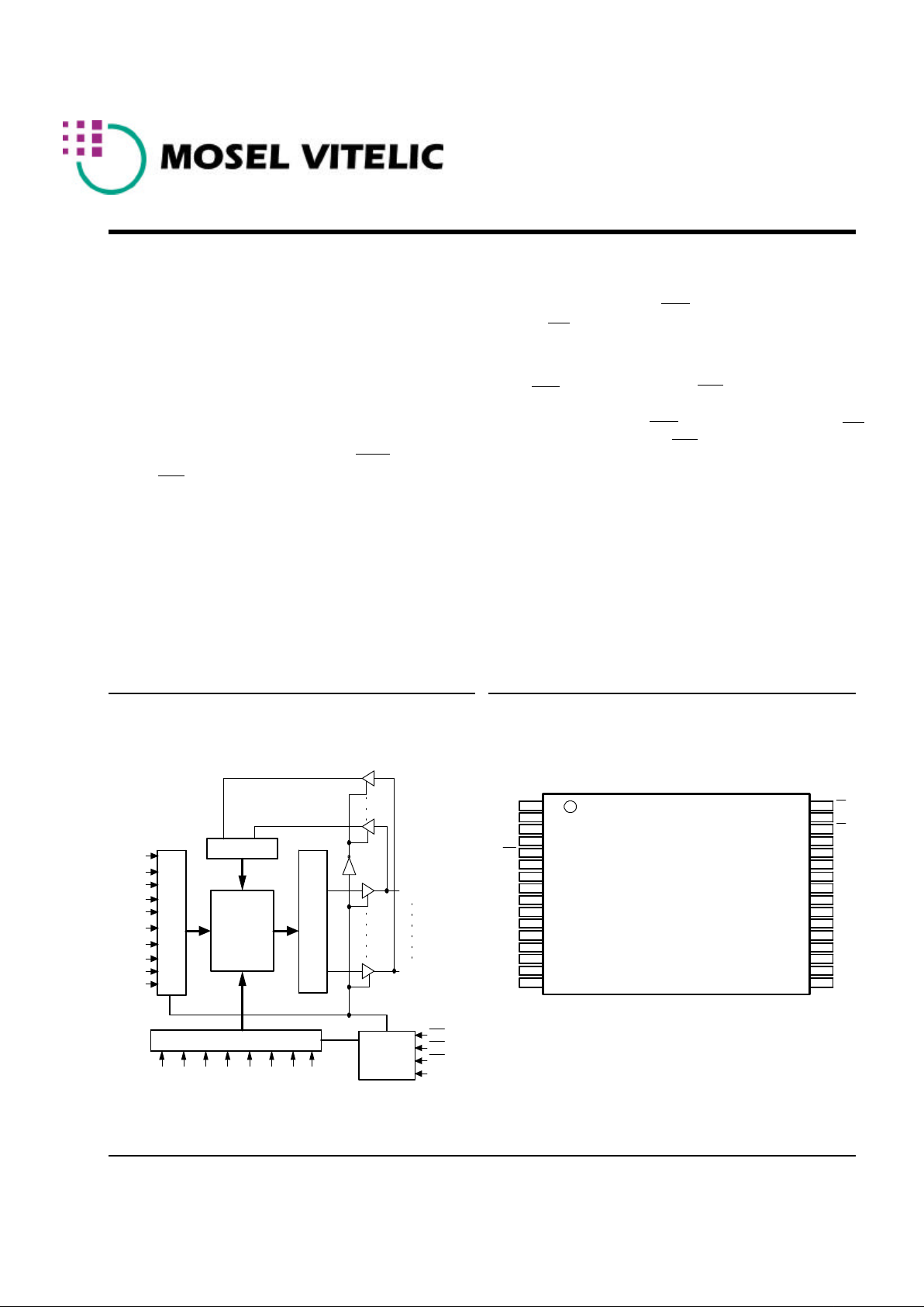
Cell Array
ROW DECODER
SENSE AMP
INPUT BUFFER
COLUMN DECODER
CONTROL
CIRCUIT
I/O8
I/O1
OE
WE
CE1
CE2
A
8
A
7
A
6
A
5
A
4
A
3
A
2
A
1
A
0
A9
A10A11A12A13A14A15A16A
17
V62C3802048L(L)
Ultra Low Power
256K x 8 CMOS SRAM
Features
• Low-power consumption
- Active: 40mA at 35ns
- Stand-by: 10
µA
(CMOS input/output)
2 µA CMOS input/output, L version
• Single + 2.7 to 3.3V Power Supply
• Equal access and cycle time
• 35/45/55/70/85/100 ns access time
• Easy memory expansion with CE1
, CE2
and OE
inputs
• 1.0V data retention mode
• TTL compatible, Tri-state input/output
• Automatic power-down when deselected
• Package available: 32-TSOP1 / STSOP
• 48 Ball CSP_BGA
Functional Description
The V62C3802048L is a low power CMOS Static RAM organized as 262,144 words by 8 bits. Easy memory expansion is provided by an active LOW CE1
, an active HIGH CE2, an acti-
ve LOW OE
, and Tri-state I/O’s. This device has an autom-
atic power-down mode feature when deselected.
Writing to the device is accomplished by taking Chip En-
able 1 (CE1
) with Write Enable (WE ) LOW, and Chip Enable 2 (CE2) HIGH. Reading from the device is performed by
taking Chip Enable 1 (CE1
) with Output Enable (OE)
LOW while Write Enable (WE ) and Chip Enable 2 (CE2)
is HIGH. The I/O pins are placed in a high-impedance state when the device is deselected: the outputs are disabled during a write cycle.
The V62C3802048LL comes with a 1V data retention feature
and Lower Standby Power. The V62C3802048L is available in
a 32-pin 8 x 20 mm TSOP1/8 x 13.4mm STSOP and CSP type
48-fpBGA packages.
32-Pin TSOP1 / STSOP(CSP_BGA see next page)
Logic Block Diagram
REV. 1.2 May 2001 V62C3802048L(L)
1
Page 2
2
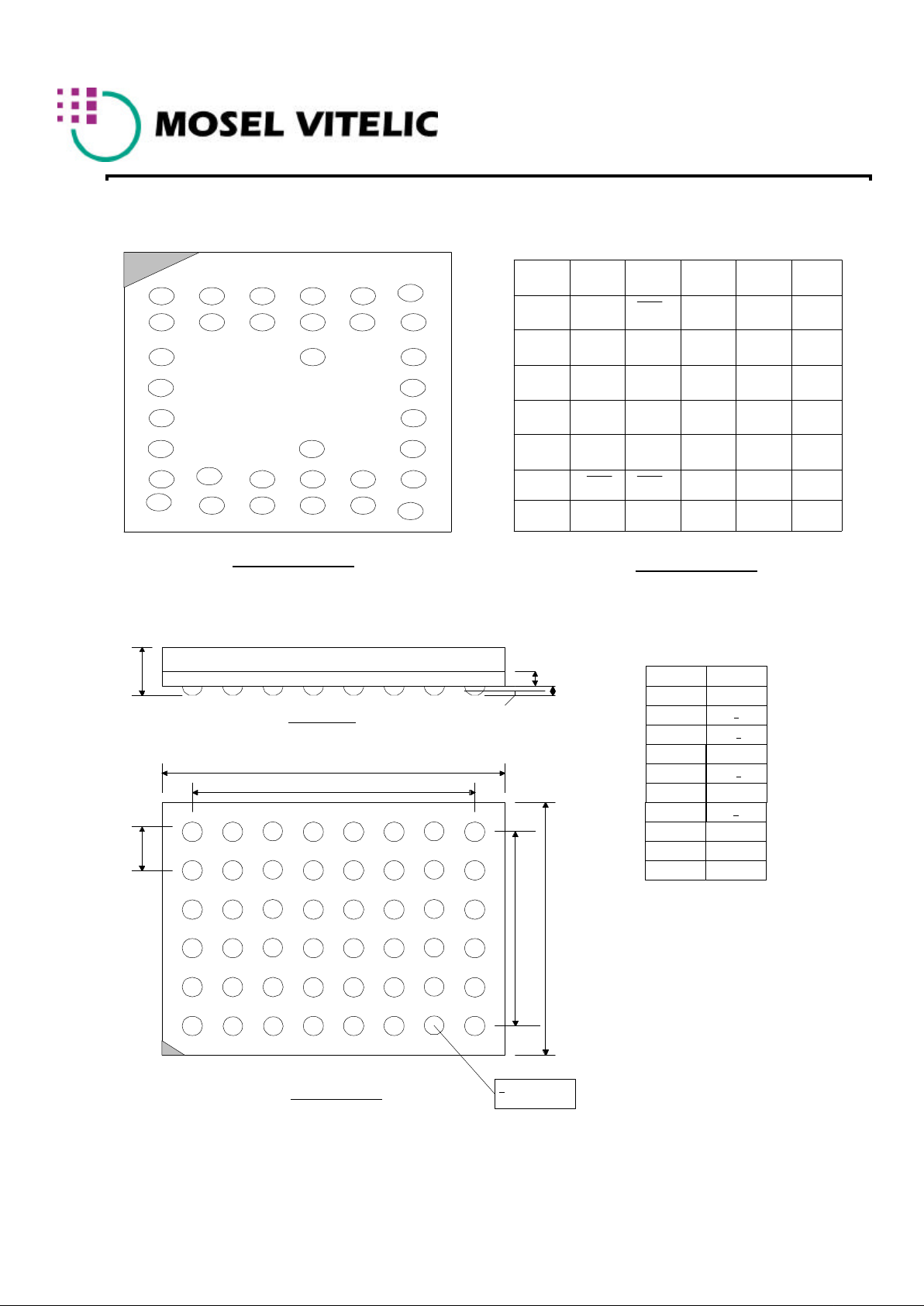
1 2 3 4 5 6
MOSEL VITELIC V62C3802048L(L)B
1 2 3 4 5 6
A
B
C
D
E
F
G
H
A0
I/O5
I/O6
VSS
VCC
I/O7
I/O8
A9
A1
A2
NC
NC
NC
NC
OE
A10
CS2
WE
NC
NC
NC
NC
CS1
A11
A3
A4
A5
NC
NC
A17
A16
A12
A6
A7
NC
NC
NC
NC
A15
A13
A8
I/O1
I/O2
VCC
VSS
I/O3
I/O4
A14
Top View
Note: NC means no Ball.
Top View
SIDE VIEW
BOTTOM VIEW
48 Ball - 9x12 fpBGA (Ultra Low Power)
PACKAGE OUTLINE DWG.
SYMBOL
UNIT:MM
A
D
D1
e
E1
E
C
A1
6
5
4
3
2
1
A B C D E F G H
aaa
b
SOLDER BALL
A
1.05+0.15
A1
0.25+
0.05
0.35+
.05
0.30(TYP)
12.00+
0.10
5.25
9.00+
0.10
b
c
D
D1
E
E1
e
aaa
3.75
0.75TYP
0.10
V62C3802048L(L)
REV. 1.2 May 2001 V62C3802048L(L)
Page 3
Absolute Maximum Ratings *
* Note: Stresses greater than those listed above Absolute Maximum Ratings may cause permanent damage to the device. This is a stress rating only and functional operation of the device at these or any conditions outside those indicated in the operational sections of this specification is not implied. Exposure to absolute maximum rating conditions for extended periods may affect reliability.
Parameter Symbol Minimum Maximum Unit
Voltage on Any Pin Relative to Gnd Vt -0.5 4.6 V
Power Dissipation P
T
− 1.0 W
Storage Temperature (Plastic) Tstg -55 +150
0
C
Temperature Under Bias Tbias -40 +85
0
C
Truth Table
* Key: X = Don’t Care, L = Low, H = High
CE1 CE2 WE OE Data Mode
H X X X High-Z Standby
X L X X High-Z Standby
L H H L Data Out Active, Read
L H H H High-Z Active, Output Disable
L H L X Data In Active, Write
3
Recommended Operating Conditions (T
A
= 00C to +700C / -400C to 850C**)
* VIL min = -2.0V for pulse width less than tRC/2.
** For Industrial Temperature.
Parameter Symbol Min Typ Max Unit
V
CC
2.7 3.0 3.3 V
Gnd 0.0 0.0 0.0 V
V
IH
2.2 - VCC + 0.2 V
V
IL
-0.5* - 0.6 V
Supply Voltage
Input Voltage
V62C3802048L(L)
REV. 1.2 May 2001 V62C3802048L(L)
Page 4
AC Test Conditions
Input Pulse Level 0.6V to 2.2V
Input Rise and Fall Time 5ns
Input and Output Timing
Reference Level 50% of input level
(VIL+VIH)/2
Output Load Condition
70ns/85 ns C
L
= 30pf + 1TTL Load
Load 100ns/120 ns C
L
= 100pf + 1TTL Load
C
L
*
Figure A. * Including Scope and Jig Capacitance
DC Operating Characteristics (V
cc
= 2.7 to 3.3V, Gnd = 0V, TA = 00C to +700C / -400C to 850C)
Input Leakage Current
IILII
Vcc = Max,
V
in
= Gnd to V
cc
- 1 - 1 - 1 - 1 µA
Output Leakage
Current
IILOI
CE1 = VIH or CE2 = V
IL
Vcc= Max, V
OUT
= Gnd to V
cc
- 1 - 1 - 1 - 1 µA
Operating Power
Supply Current
I
CC
CE1 = VIL , CE2 = V
IH
VIN = V
IH
or V
IL
, I
OUT
= 0 mA
- 3 - 3 - 3 - 3
mA
Average Operating
Current
I
CC1
CE1 = VIL , CE2 = V
IH
I
OUT
= 0mA,
Min Cycle, 100% Duty
- 35 - 35 - 30 - 25
mA
I
CC2
CE1 = 0.2V ,
CE2 =V
cc
- 0.2V
I
OUT
= 0mA,
Cycle Time=1µs, 100% Duty
- 3 - 3 - 3 - 3 mA
Standby Power Supply
Current (TTL Level)
I
SB
CE1 = VIH or CE2 = VIL - 0.5 - 0.5 - 0.5 - 0.5 mA
Standby Power Supply
Current (CMOS Level)
I
SB1
CE1 > Vcc - 0.2V or
CE2 <
0.2V, f = 0
V
IN
< 0.2V or
V
IN
> Vcc- 0.2V L
-
-
10
2
-
-
10
2
--10
2
-
-
102µA
µA
Output Low Voltage V
OL
IOL = 2 mA - 0.4 - 0.4 - 0.4 - 0.4 V
Output High Voltage V
OH
IOH = -2 mA 2.4 - 2.4 - 2.4 - 2.4 - V
-55 -85 -100
Unit
Parameter Sym Test Conditions
Min Max Min Max Min Max Min Max
-70
4
Capacitance (f = 1MHz, T
A
= 250C)
* This parameter is guaranteed by device characterization and is not production tested.
Parameter* Symbol Test Condition Max Unit
Input Capacitance
C
in
Vin = 0V 7 pF
I/O Capacitance
C
I/O
V
in
= V
out
= 0V 8 pF
V62C3802048L(L)
REV. 1.2 May 2001 V62C3802048L(L)
Page 5

DC Operating Characteristics (V
cc
= 2.7 to 3.3V, Gnd = 0V, TA = 00C to +700C / -400C to 850C)
-35 -45
Input Leakage Current
IILII
Vcc = Max,
V
in
= Gnd to V
cc
- 1 - 1 µA
Output Leakage
Current
IILOI
CE1 = VIH or CE2 = V
IL
Vcc= Max, V
OUT
= Gnd to V
cc
- 1 - 1 µA
Operating Power
Supply Current
I
CC
CE1 = VIL , CE2 = V
IH
VIN = V
IH
or V
IL
, I
OUT
= 0 mA
- 3 - 3
mA
Average Operating
Current
I
CC1
CE1 = VIL , CE2 = V
IH
I
OUT
= 0mA,
Min Cycle, 100% Duty
- 40 - 40
mA
I
CC2
CE1 = 0.2V ,
CE2 =V
cc
- 0.2V
I
OUT
= 0mA,
Cycle Time=1µs, 100% Duty
- 3 - 3 mA
Standby Power Supply
Current (TTL Level)
I
SB
CE1 = VIH or CE2 = VIL - 0.5 - 0.5 mA
Standby Power Supply
Current (CMOS Level)
I
SB1
CE1 > Vcc - 0.2V or
CE2 <
0.2V, f = 0
V
IN
< 0.2V or
V
IN
> Vcc- 0.2V L
-
-
10
2
--102µA
µA
Output Low Voltage V
OL
IOL = 2 mA - 0.4 - 0.4 V
Output High Voltage V
OH
IOH = -2 mA 2.4 - 2.4 - V
Unit
Parameter Sym Test Conditions
5
Min Max Min Max
V62C3802048L(L)
REV. 1.2 May 2001 V62C3802048L(L)
Page 6

Parameter Symbol
Unit
Note
Read Cycle Time
t
RC
55 - 70 - 85 - 100 - ns
Address Access Time
tAA - 55 - 70 - 85 - 100 ns
Chip Enable Access Time
t
ACE
- 55 - 70 - 85 - 100 ns
Output Enable Access Time
t
OE
- 40 - 40 - 40 - 50 ns
Output Hold from Address Change
t
OH
10 - 10 - 10 - 10 - ns
Chip Enable to Output in Low-Z
t
CLZ
10 - 10 - 10 - 10 - ns 4,5
Chip Disable to Output in High-Z
t
CHZ
- 25 - 30 - 35 - 40 ns 4,5
Output Enable to Output in Low-Z
t
OLZ
5 - 5 - 5 - 5 - ns 4,5
Output Disable to Output in High-Z
t
OHZ
- 20 - 25 - 30 - 35 ns 4,5
Power-Up Time
t
PU
0 - 0 - 0 - 0 - ns 5
Power-Down Time
t
PD
- 55 - 70 - 85 - 100 ns 5
Read Cycle
(3,9)
(V
cc
= 2.7 to3.3V, Gnd = 0V, TA = 00C to +700C / -400C to +850C)
Write Cycle
(3,11)
(V
cc
= 2.7 to 3.3V, Gnd = 0V, T
A
= 00C to +700C / -400C to +850C)
Parameter Symbol
Unit
Note
Write Cycle Time
t
WC
55 - 70 - 85 - 100 - ns
Chip Enable to Write End
tCW 40 - 60 - 70 - 80 - ns
Address Setup to Write End
t
AW
40 - 60 - 70 - 80 - ns
Address Setup Time
t
AS
0 - 0 - 0 - 0 - ns
Write Pulse Width
t
WP
40 - 50 - 60 - 70 - ns
Write Recovering Time
t
WR
0 - 0 - 0 - 0 - ns
Data Valid to Write End
t
DW
25 - 30 - 35 - 40 - ns
Data Hold Time
t
DH
0 - 0 - 0 - 0 - ns
Write Enable to Output in High-Z
t
WZ
- 25 - 30 - 35 - 40 ns 4,5
Output Active from Write End
t
OW
5 - 5 - 5 - 5 - ns 4,5
Min Max Min Max Min Max Min Max
-55 -70 -85 -100
6
Min Max Min Max Min Max Min Max
-55 -70 -85 -100
V62C3802048L(L)
REV. 1.2 May 2001 V62C3802048L(L)
Page 7

Parameter Symbol
-35 -45
Unit
Note
Read Cycle Time
t
RC
35 - 45 - ns
Address Access Time
tAA - 35 - 45 ns
Chip Enable Access Time
t
ACE
- 35 - 45 ns
Output Enable Access Time
t
OE
- 20 - 20 ns
Output Hold from Address Change
t
OH
5 - 5 - ns
Chip Enable to Output in Low-Z
t
CLZ
5 - 5 - ns 4,5
Chip Disable to Output in High-Z
t
CHZ
- 20 - 25 ns 4,5
Output Enable to Output in Low-Z
t
OLZ
5 - 5 - ns 4,5
Output Disable to Output in High-Z
t
OHZ
- 15 - 20 ns 4,5
Power-Up Time
t
PU
0 - 0 - ns 5
Power-Down Time
t
PD
- 35 - 45 ns 5
Read Cycle
(3,9)
(V
cc
= 2.7 to3.3V, Gnd = 0V, TA = 00C to +700C / -400C to +850C)
Write Cycle
(3,11)
(V
cc
= 2.7 to 3.3V, Gnd = 0V, T
A
= 00C to +700C / -400C to +850C)
Parameter Symbol
-35 -45
Unit
Note
Write Cycle Time
t
WC
35 - 45 - ns
Chip Enable to Write End
tCW 30 - 40 - ns
Address Setup to Write End
t
AW
30 - 40 - ns
Address Setup Time
t
AS
0 - 0 - ns
Write Pulse Width
t
WP
30 - 35 - ns
Write Recovering Time
t
WR
0 - 0 - ns
Data Valid to Write End
t
DW
20 - 25 - ns
Data Hold Time
t
DH
0 - 0 - ns
Write Enable to Output in High-Z
t
WZ
- 20 - 25 ns 4,5
Output Active from Write End
t
OW
5 - 5 - ns 4,5
Min Max Min Max
7
Min Max Min Max
V62C3802048L(L)
REV. 1.2 May 2001 V62C3802048L(L)
Page 8

Timing Waveform of Read Cycle 1
(3,6,7,9)
(Address Controlled)
t
RC
t
AA
t
OH
Data Valid
Address
D
OUT
Timing Waveform of Read Cycle 2
(5,6,8,9)
(CE1 Controlled)
50% 50%
I
CC
I
SB
t
PD
t
CHZ
t
OHZ
t
RC
t
OE
t
OLZ
t
ACE
t
CLZ
t
PU
CE1
OE
D
OUT
Supply Current
Data Valid
Timing Waveform of Read Cycle 3
(3,6,8,9)
(CE2 Controlled)
50% 50%
I
CC
I
SB
t
PD
t
CHZ
t
OHZ
t
RC
t
OE
t
OLZ
t
ACE
t
CLZ
t
PU
CE2
OE
D
OUT
Supply Current
Data Valid
8
V62C3802048L(L)
REV. 1.2 May 2001 V62C3802048L(L)
Page 9

Timing Waveform of Write Cycle 1
(10,11)
(WE Controlled)
Data Valid
Address
D
OUT
Timing Waveform of Write Cycle 2
(10,11)
(CE1 Controlled)
Timing Waveform of Write Cycle 3
(10,11)
(CE2 Controlled)
D
IN
WE
t
DW
t
DH
t
OW
t
WZ
t
AS
t
WP
t
WR
t
WC
t
AW
D
OUT
D
IN
WE
Address
CE1
Data Valid
t
WZ
t
DW
t
DH
t
WP
t
WC
t
CW
t
AW
t
WR
t
AS
D
OUT
D
IN
WE
Address
CE2
Data Valid
t
WZ
t
DW
t
DH
t
WP
t
WC
t
CW
t
AW
t
WR
t
AS
9
V62C3802048L(L)
REV. 1.2 May 2001 V62C3802048L(L)
Page 10

Data Retention Characteristics (L Version Only)
(1)
Parameter Symbol Test Condition Min Max Unit
VCC for Data Retention
V
DR
CE1 > VCC - 0.2V or 1.0
-
V
Data Retention Current
I
CCDR
CE
2
< + 0.2V
- 1
µA
Chip Deselect to Data Retention Time
t
CDR
VIN > VCC - 0.2V or 0 - ns
Operation Recovery Time
(2)
t
R
VIN < 0.2V
t
RC
- ns
Data Retention Mode
V
DR
> 1.0V
Vcc_typ
V
IH
V
IH
V
DR
V
CC
CE
t
R
t
CDR
Vcc_typ
Data Retention Waveform (L Version Only) (T
A
= 00C to +700C / -400C to +850C)
10
Notes
1. L-version includes this feature.
2. This Parameter is samples and not 100% tested.
3. For test conditions, see AC Test Condition, Figure A.
4. This parameter is tested with CL = 5
pF as shown in Figure B. Transition is measured + 500mV from steady-state voltage.
5. This parameter is guaranteed, but is not tested.
6. WE
is HIGH for read cycle.
7. CE1
and OE are LOW and CE2 is HIGH for read cycle.
8. Address valid prior to or coincident with CE1
transition LOW or CE2 transition HIGH.
9. All read cycle timings are referenced from the last valid address to the first transtion address.
10. CE1
or WE must be HIGH or CE2 must be LOW during address transition.
11. All write cycle timings are referenced from the last valid address to the first transition address.
V62C3802048L(L)
REV. 1.2 May 2001 V62C3802048L(L)
Page 11

V62C3802048L(L)
Ordering Information
Device Type* Speed Package
V62C3802048L-35V 35 ns 8x13.4 mm 32-pin Plastic STSOP
V62C3802048L-45V 45 ns
V62C3802048L-55V 55 ns
V62C3802048L-70V 70 ns
V62C3802048L-85V 85 ns
V62C3802048L-100V 100 ns
V62C3802048LL-35V 35 ns
V62C3802048LL-45V 45 ns
V62C3802048LL-55V 55 ns
V62C3802048LL-70V 70 ns
V62C3802048LL-85V 85 ns
V62C3802048LL-100V 100 ns
V62C3802048L-35T 35 ns 8 x 20 mm 32-pin Plastic TSOP1
V62C3802048L-45T 45 ns
V62C3802048L-55T 55 ns
V62C3802048L-70T 70 ns
V62C3802048L-85T 85 ns
V62C3802048L-100T 100 ns
V62C3802048LL-35T 35 ns
V62C3802048LL-45T 45 ns
V62C3802048LL-55T 55 ns
V62C3802048LL-70T 70 ns
V62C3802048LL-85T 85 ns
V62C3802048LL-100T 100 ns
V62C3802048L(L)-35B 35 ns CSP type 48-fpBGA
V62C3802048L(L)-45B 45 ns
V62C3802048L(L)-55B 55 ns
V62C3802048L(L)-70B 70 ns
V62C3802048L(L)-85B 85 ns
V62C3802048L(L)-100B 100 ns
11
* For Industrial Temperature tested devices, an “I” designator will be added to the end of the Device number.
REV. 1.2 May 2001 V62C3802048L(L)
Page 12

MOSEL VITELIC
WORLDWIDE OFFICES
© Copyright 2001, MOSEL VITELIC Inc.
5/01
Printed in U.S.A.
MOSEL VITELIC
3910 N. First Street, San Jose, CA 95134-1501 Ph: (408) 433-6000 Fax: (408) 433-0952 Tlx: 371-9461
The information in this document is subject to change without
notice.
MOSEL VITELIC makes no commitment to update or keep current the information contained in this document. No part of this
document may be copied or reproduced in any form or by any
means without the prior written consent of MOSEL-VITELIC.
MOSEL VITELIC subjects its products to normal quality control
sampling techniques which are intended to provide an assurance
of high quality products suitable for usual commercial applications. MOSEL VITELIC does not do testing appropriate to provide
100% product quality assurance and does not assume any liability for consequential or incidental arising from any use of its products. If such products are to be used in applications in which
personal injury might occur from failure, purchaser must do its
own quality assurance testing appropriate to such applications.
U.S. SALES OFFICES
U.S.A.
3910 NORTH FIRST STREET
SAN JOSE, CA 95134
PHONE: 408-433-6000
FAX: 408-433-0952
TAIWAN
7F, NO. 102
MIN-CHUAN E. ROAD, SEC. 3
TAIPEI
PHONE: 886-2-2545-1213
FAX: 886-2-2545-1209
NO 19 LI HSIN ROAD
SCIENCE BASED IND. PARK
HSIN CHU, TAIWAN, R.O.C.
PHONE: 886-3-579-5888
FAX: 886-3-566-5888
SINGAPORE
10 ANSON ROAD #23-13
INTERNATIONAL PLAZA
SINGAPORE 079903
PHONE: 65-3231801
FAX: 65-3237013
JAPAN
ONZE 1852 BUILDING 6F
2-14-6 SHINTOMI, CHUO-KU
TOKYO 104-0041
PHONE: 03-3537-1400
FAX: 03-3537-1402
UK & IRELAND
SUITE 50, GROVEWOOD
BUSINESS CENTRE
STRATHCLYDE BUSINESS
PARK
BELLSHILL, LANARKSHIRE,
SCOTLAND, ML4 3NQ
PHONE: 44-1698-748515
FAX: 44-1698-748516
GERMANY
(CONTINENTAL
EUROPE & ISRAEL)
BENZSTRASSE 32
71083 HERRENBERG
GERMANY
PHONE: +49 7032 2796-0
FAX: +49 7032 2796 22
NORTHWESTERN
3910 NORTH FIRST STREET
SAN JOSE, CA 95134
PHONE: 408-433-6000
FAX: 408-433-0952
SOUTHWESTERN
302 N. EL CAMINO REAL #200
SAN CLEMENTE, CA 92672
PHONE: 949-361-7873
FAX: 949-361-7807
CENTRAL,
NORTHEASTERN &
SOUTHEASTERN
604 FIELDWOOD CIRCLE
RICHARDSON, TX 75081
PHONE: 214-826-6176
FAX: 214-828-9754
V62C3802048L(L)
 Loading...