

Datasheet V62C1162048LL-100T, V62C1162048LL-100M, V62C1162048LL-100B, V62C1162048L-85T, V62C1162048L-85M Datasheet (Mosel Vitelic)
...Page 1
V62C1162048L(L)
Ultra Low Power
128K x 16 CMOS SRAM
Features
• Low-power consumption
- Active: 35mA I
- Stand-by: 10
2
at 70ns
CC
µA (CMOS input/output)
µA (CMOS input/output, L version)
• 70/85/100/120 ns access time
• Equal access and cycle time
• Single +1.8V to2.2V Power Supply
• Tri-state output
• Automatic power-down when deselected
• Multiple center power and ground pins for
improved noise immunity
• Individual byte controls for both Read and
Write cycles
• Available in 44 pin TSOPII / 48-fpBGA / 48-µBGA
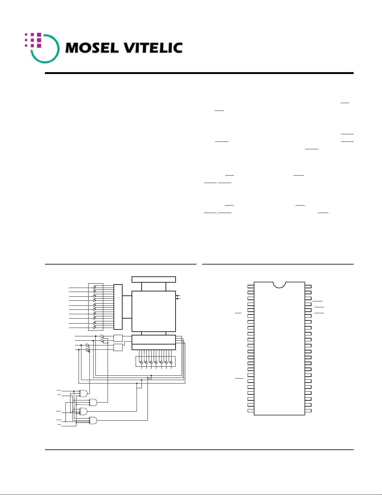
Logic Block Diagram
Functional Description
The V62C1162048L is a Low Power CMOS Static
RAM organized as 131,072 words by 16 bits. Easy
Memory expansion is provided by an active LOW (CE)
and (OE) pin.
This device has an automatic power-down mode feature
when deselected. Separate Byte Enable controls (BLE
and BHE) allow individual bytes to be accessed. BLE
controls the lower bits I/O1 - I/O8. BHE controls the
upper bits I/O9 - I/O16.
Writing to these devices is performed by taking Chip
Enable (CE
(BLE
) with Write Enable (WE) and Byte Enable
/BHE) LOW.
Reading from the device is performed by taking Chip
Enable (CE
(BLE
) with Output Enable (OE) and Byte Enable
/BHE) LOW while Write Enable (WE
) is held
HIGH.
TSOPII / 48-fpBGA / 48-µBGA (See nest page)
BHE
BLE
WE
OE
CE
A0
A1
A2
A3
A4
A5
A6
A7
A8
A9
I/O1 - I/O8
I/O9 - I/O16
Row Select
Data
Cont
Data
Cont
Pre-Charge Circuit
Memory Array
1024 X 2048
I/O Circuit
Column Select
A10 A11 A12 A13 A14
A15 A16
1
Vcc
Vss
A3
A2
A1
A0
CE
I/O1
I/O2
I/O3
I/O4
Vcc
Vss
I/O5
I/O6
I/O7
I/O8
WE
A16
A15
A14
A13 A11
2
3
4
5
6
7
8
9
10
11
12
13
14
15
16
17
18
19
20
21
A12
44
A5A4
43
A6
42
A7
OE
41
BHE
40
BLE
39
I/O16
38
I/O15
37
I/O14
36
I/O13
35
Vss
34
Vcc
33
I/O12
32
I/O11
31
I/O10
30
I/O9
29
NC
28
27A9A8
26
A10
25
24
NC
2322
1
REV. 1.2 May 2001 V62C1162048L(L)
Page 2
MOSEL VITELIC V62C1162048L(L)M
V62C1162048L(L)
1
2 3 4 5 6
A
B
C
D
E
F
G
H
Top View
48 Ball - 6 x 8 µµBGA (Ultra Low Power)
1 2 3 4 5 6
BLE
I/O9
I/O10
VSS
VCC
I/O15
I/O16
NC
Note: NC means no Ball.
OE
BHE
I/O11
I/O12
I/O13
I/O14
NC
A8
A0
A3
A5
NC
NC
A14
A12
A9
A1
A4
A6
A7
A16
A15
A13
A10
A2
CE
I/O2
I/O4
I/O5
I/O6
WE
A11
Top View
PACKAGE OUTLINE DWG.
NC
I/O1
I/O3
VCC
VSS
I/O7
I/O8
NC
C
A1
A
6
e
5
4
3
2
1
A B C D E F G H
SIDE VIEW
D
D1
BOTTOM VIEW
aaa
b
SOLDER BALL
E
E1
SYMBOL
A
A1
b
c
D
D1
E
E1
e
aaa
UNIT:MM
1.10+
0.10
0.22+0.05
0.35
0.36(TYP)
8.00+
0.10
5.25
6.00+
0.10
3.75
0.75TYP
0.10
REV. 1.2 May 2001 V62C1162048L(L)
2
Page 3
V62C1162048L(L)
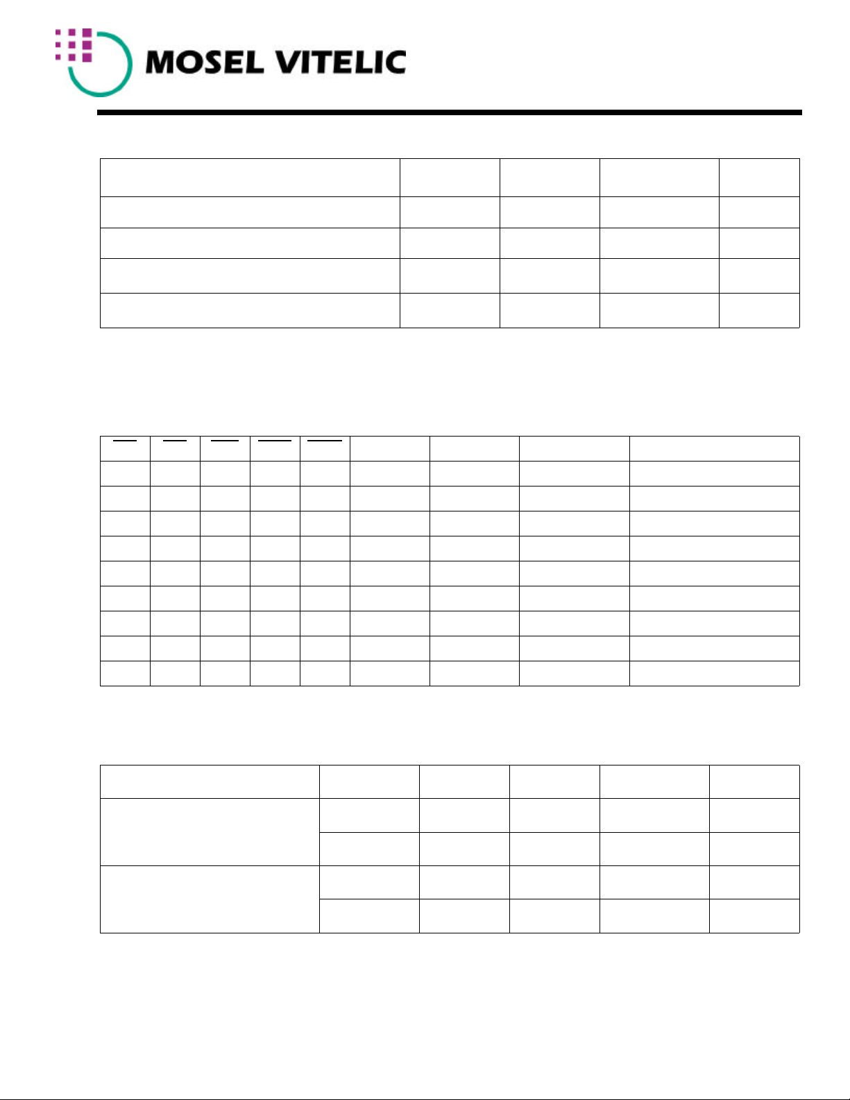
Absolute Maximum Ratings *
Parameter Symbol Minimum Maximum Unit
Voltage on Any Pin Relative to Gnd Vt -0.5 +4.0 V
Power Dissipation PT − 1.0 W
Storage Temperature (Plastic) Tstg -55 +150
Temperature Under Bias Tbias -40 +85
* Note: Stresses greater than those listed above Absolute Maximum Ratings may cause permanent damage to the device. This is a stress rating only and function operation of the device at these or any other conditions outside those indicated in the operational sections of this specification is not implied. Exposure to absolute maximum rating conditions for extended periods may affect reliability.
0
C
0
C
Truth Table
CE OE WE BLE BHE I/O1-I/O8 I/O9-I/O16 Power Mode
H X X X X High-Z High-Z Standby Standby
L L H L H Data Out High-Z Active Low Byte Read
L L H H L High-Z Data Out Active High Byte Read
L L H L L Data Out Data Out Active Word Read
L X L L L Data In Data In Active Word Write
L X L L H Data In High-Z Active Low Byte Write
L X L H L High-Z Data In Active High Byte Write
L H H X X High-Z High-Z Active Output Disable
L X X H H High-Z High-Z Active Output Disable
* Key: X = Don’t Care, L = Low, H = High
Recommended Operating Conditions (T
Parameter Symbol Min Typ Max Unit
Supply Voltage
Input Voltage
* VIL min = -2.0V for pulse width less than tRC/2.
** For Industrial Temperature
REV. 1.2 May 2001 V62C1162048L(L)
= 0oC to +70oC / -40oC to 85oC**)
A
V
CC
1.8 2.0 2.2 V
Gnd 0.0 0.0 0.0 V
V
IH
V
IL
1.6 - VCC + 0.2 V
-0.5* - 0.4 V
3
Page 4
DC Operating Characteristics (V
V62C1162048L(L)
=1.8 to 2.2V, Gnd = 0V, TA = 00C to +700C / -400C to 850C)
cc
Parameter Sym Test Conditions
Input Leakage Current
Output Leakage
Current
Operating Power
Supply Current
Average Operating
Current
Standby Power Supply
Current (TTL Level)
Standby Power Supply
Current (CMOS Level)
Vcc = Max,
IILII
IILOI
I
CC
I
CC1
= Gnd to V
V
in
cc
CE = VIH or Vcc= Max,
V
= Gnd to V
OUT
CE = VIL , VIN = V
I
= 0
OUT
I
= 0mA,
OUT
cc
or V
IH
,
IL
Min Cycle, 100% Duty
CE < 0.2V
I
CC2
I
SB
I
SB1
= 0mA,
I
OUT
Cycle Time=1µs, Duty=100%
CE = VIH - 0.5 - 0.5 - 0.5 - 0.5 mA
CE > Vcc - 0.2V
V
< 0.2V or
IN
V
> Vcc- 0.2V L
IN
-70 -100
Min Max Min Max Min Max Min Max
-85
-120
Unit
- 1 - 1 - 1 - 1 µA
- 1 - 1 - 1 - 1 µA
- 5 - 5 - 5 - 5
- 35 - 35 - 30 - 30 mA
- 3 - 3 - 3 - 3 mA
-
10
-
-
10
2
-
-
10
-
102µA
2
-
2
-
mA
µA
Output Low Voltage V
Output High Voltage V
Capacitance (f = 1MHz, T
IOL = 2 mA - 0.4 - 0.4 - 0.4 - 0.4 V
OL
IOH = -1 mA 1.6 - 1.6 - 1.6 - 1.6 - V
OH
= 250C)
A
Parameter* Symbol Test Condition Max Unit
Input Capacitance
I/O Capacitance
* This parameter is guaranteed by device characterization and is not production tested.
AC Test Conditions
Input Pulse Level 0.4V to 1.6V
Input Rise and Fall Time 5ns
Input and Output Timing
Reference Level 1.0V
Output Load Condition
70ns/85ns C
Load for 100ns/120ns C
= 30pf + 1TTL Load
L
= 100pf + 1TTL Load
L
C
in
C
I/O
V
Vin = 0V 7 pF
= V
in
C
Figure A. * Including Scope and Jig Capacitance
= 0V 8 pF
out
*
L
TTL
REV. 1.2 May 2001 V62C1162048L(L)
4
Page 5

V62C1162048L(L)
Read Cycle
(9)
(V
= 1.8 to 2.2V, Gnd = 0V, TA = 00C to +700C / -400C to +850C)
cc
Parameter Sym
Read Cycle Time
Address Access Time
Chip Enable Access Time
Output Enable Access Time
Output Hold from Address Change
Chip Enable to Output in Low-Z
Chip Disable to Output in High-Z
Output Enable to Output in Low-Z
Output Disable to Output in High-Z
BLE
, BHE Enable to Output in Low-Z
BLE, BHE Disable to Output in High-Z
-70 -85 -100 -120
Unit
Min Max Min Max Min Max Min Max
t
RC
tAA - 70 - 85 - 100 - 120 ns
t
ACE
t
OE
t
OH
t
LZ
t
HZ
t
OLZ
t
OHZ
t
BLZ
t
BHZ
70 - 85 - 100 - 120 - ns
- 70 - 85 - 100 - 120 ns
- 40 - 40 - 50 - 60 ns
10 - 10 - 10 - 10 - ns
10 - 10 - 10 - 10 - ns 4,5
- 30 - 35 - 40 - 45 ns 3,4,5
5 - 5 - 5 - 5 - ns
- 25 - 30 - 35 - 40 ns
5 - 5 - 5 - 5 - ns 4,5
- 25 - 30 - 35 - 40 ns 3,4,5
Note
BLE, BHE Access Time
Write Cycle
(11)
(V
= 1.8 to 2.2V, Gnd = 0V, TA = 00C to +700C / -400C to +850C)
cc
Parameter Symbol
Write Cycle Time
Chip Enable to Write End
Address Setup to Write End
Address Setup Time
Write Pulse Width
Write Recovery Time
Data Valid to Write End
Data Hold Time
Write Enable to Output in High-Z
Output Active from Write End
t
BA
- 40 - 40 - 50 - 60 ns
-70 -85 -100 -120
Unit
Min Max Min Max Min Max Min Max
t
WC
tCW 60 - 70 - 80 - 90 - ns
t
AW
t
AS
t
WP
t
WR
t
DW
t
DH
t
WHZ
t
OW
70 - 85 -
60 - 70 - 80 - 90 - ns
0 - 0 - 0 - 0 - ns
50 - 60 - 70 - 80 - ns
0 - 0 - 0 - 0 - ns
30 - 35 - 40 - 45 - ns
0 - 0 - 0 - 0 - ns
- 30 - 35 - 40 - 45 ns
5 - 5 - 5 - 5 - ns
100
- 120 - ns
Note
BLE, BHE Setup to Write End
REV. 1.2 May 2001 V62C1162048L(L)
t
BW
60 - 70 - 80 - 90 - ns
5
Page 6

V62C1162048L(L)
Timing Waveform of Read Cycle 1
(Address Controlled)
Address
t
OH
Data Out
Previous Data Valid
Timing Waveform of Read Cycle 2
Address
t
AA
t
ACE
CE
t
LZ(4,5)
t
BA
(BLE/BHE)
t
BLZ(4,5)
t
OE
OE
t
RC
t
AA
Data Valid
t
RC
t
HZ(3,4,5)
t
BHZ(3,4,5)
t
OHZ
Data Out
Notes (Read Cycle)
1. WE are high for read cycle.
2. All read cycle timing is referenced from the last valid address to the first transition address.
3.
t
and t
HZ
4. At any given temperature and voltage condition
device.
5. Transition is measured +
6. Device is continuously selected with CE
7. Address valid prior to coincident with CE
8. For common I/O applications, minimization or elimination of bus contention conditions is necessary during read and write
cycle.
9. For test conditions, see AC Test Condition, Figure A.
REV. 1.2 May 2001 V62C1162048L(L)
are defined as the time at which the outputs achieve the open circuit condition referenced to VOH or VOL levels.
OHZ
200mV from steady state voltage with load. This parameter is sampled and not 100% tested.
High-Z
t
OLZ
t
(max.) is less than tLZ (min.) both for a given device and from device to
HZ
= VIL.
transition Low.
t
OH
Data Valid
6
Page 7

V62C1162048L(L)
Timing Waveform of Write Cycle 1
Address
CE
BLE/BHE
WE
Data In
High-Z
Data Out
Timing Waveform of Write Cycle 2
Address
CE
t
AS (4)
BLE/BHE
t
AS (4)
(Address Controlled)
t
WC
t
AW
t
CW (3)
t
BW
t
WP (2)
t
OHZ (6)
High-Z (8)
(CE Controlled)
t
WC
t
AW
t
CW (3)
t
BW
t
WR (5)
t
DW
t
DH
t
OW
t
WR (5)
WE
Data In
High-Z
Data Out
Timing Waveform of Write Cycle 3
Address
CE
t
AS (4)
BLE/BHE
WE
Data In
Data Out
High-Z
High-Z
t
WP (2)
t
DW
t
t
LZ
WHZ (6)
t
DH
High-Z (8)High-Z
(BLE/BHE Controlled)
t
WC
t
AW
t
CW (3)
t
BW
t
WP (2)
t
DW
t
t
BLZ
WHZ (6)
High-Z (8)
t
WR (5)
t
DH
REV. 1.2 May 2001 V62C1162048L(L)
7
Page 8

V62C1162048L(L)
Notes (Write Cycle)
1. All write timing is referenced from the last valid address to the first transition address.
2. A write occurs during the overlap of a low CE
low: A write ends at the earliest transition among CE
of write to the end of write.
3.
t
is measured from the later of CE going low to end of write.
CW
t
is measured from the address valid to the beginning of write.
4.
AS
5.
t
is measured from the end of write to the address change.
WR
6. If OE
Inputs of opposite phase of the output must not be applied because bus contention can occur.
7. For common I/O applications, minimization or elimination of bus contention conditions is necessary during read and
, CE and WE are in the Read Mode during this period, the I/O pins are in the output Low-Z state.
write cycle.
8. If CE
9. D
10. When CE
goes low simultaneously with WE going low or after WE going low, the outputs remain high impedance state.
OUT is the read data of the new address.
is low: I/O pins are in the outputs state. The input signals in the opposite phase leading to the output should
not be applied.
11. For test conditions, see AC Test Condition, Figure A.
and WE. A write begins at the latest transition among CE and WE going
going high and WE going high. tWP is measured from the beginning
REV. 1.2 May 2001 V62C1162048L(L)
8
Page 9

V62C1162048L(L)
Data Retention Characteristics
Parameter Symbol Test Condition Min Max Unit
VCC for Data Retention
Data Retention Current
Chip Deselect to Data Retention Time
Operation Recovery Time
Data Retention Waveform
V
CC
CE
(2)
(L Version Only) (TA = 00C to +700C / -400C to +850C)
Vcc_typ
t
CDR
V
(L Version Only)
V
DR
I
CCDR
t
CDR
t
R
Data Retention Mode
V
IH
(1)
CE > VCC - 0.2V 1.0
- 1 µA
-
VIN > VCC - 0.2V or 0 - ns
VIN < 0.2V
> 1.0V
DR
V
DR
t
V
Vcc_typ
R
IH
t
RC
- ns
V
Notes (Write Cycle)
1. L-version includes this feature.
2. This Parameter is samples and not 100% tested.
3. For test conditions, see AC Test Condition, Figure A.
4. This parameter is tested with CL = 5pF as shown in Figure B. Transition is measured +
5. This parameter is guaranteed, but is not tested.
6. WE
7. CE
8. Address valid prior to or coincident with CE
is High for read cycle.
and OE are LOW for read cycle.
transition LOW.
9. All read cycle timings are referenced from the last valid address to the first transtion address.
10. CE
or WE must be HIGH during address transition.
11. All write cycle timings are referenced from the last valid address to the first transition address.
500mV from steady-state voltage.
REV. 1.2 May 2001 V62C1162048L(L)
9
Page 10

Ordering Information
Device Type* Speed Package
V62C1162048L-70T 70 ns 44-pin TSOP Type 2
V62C1162048L-85T 85 ns
V62C1162048L-100T 100 ns
V62C1162048L-120T 120 ns
V62C1162048LL-70T 70 ns
V62C1162048LL-85T 85 ns
V62C1162048LL-100T 100 ns
V62C1162048LL-120T 120 ns
V62C1162048L(L)-70B 70 ns 48-fpBGA
V62C1162048L(L)-85B 85 ns
V62C1162048L(L)-100B 100 ns
V62C1162048L(L)-120B 120 ns
V62C1162048L(L)
V62C1162048L(L)-70M 70 ns 48V62C1162048L(L)-85M 85 ns
V62C1162048L(L)-100M 100 ns
V62C1162048L(L)-120M 120 ns
* For Industrial temperature tested devices, an “I” designator will be added to the end of the device number.
µBGA
REV. 1.2 May 2001 V62C1162048L(L)
10
Page 11

MOSEL VITELIC
WORLDWIDE OFFICES
V62C1162048L(L)
U.S.A.
3910 NORTH FIRST STREET
SAN JOSE, CA 95134
PHONE: 408-433-6000
FAX: 408-433-0952
NORTHWESTERN
3910 NORTH FIRST STREET
SAN JOSE, CA 95134
PHONE: 408-433-6000
FAX: 408-433-0952
TAIWAN
7F, NO. 102
MIN-CHUAN E. ROAD, SEC. 3
TAIPEI
PHONE: 886-2-2545-1213
FAX: 886-2-2545-1209
NO 19 LI HSIN ROAD
SCIENCE BASED IND. PARK
HSIN CHU, TAIWAN, R.O.C.
PHONE: 886-3-579-5888
FAX: 886-3-566-5888
U.S. SALES OFFICES
SOUTHWESTERN
302 N. EL CAMINO REAL #200
SAN CLEMENTE, CA 92672
PHONE: 949-361-7873
FAX: 949-361-7807
SINGAPORE
10 ANSON ROAD #23-13
INTERNATIONAL PLAZA
SINGAPORE 079903
PHONE: 65-3231801
FAX: 65-3237013
JAPAN
ONZE 1852 BUILDING 6F
2-14-6 SHINTOMI, CHUO-KU
TOKYO 104-0041
PHONE: 03-3537-1400
FAX: 03-3537-1402
CENTRAL,
NORTHEASTERN &
SOUTHEASTERN
604 FIELDWOOD CIRCLE
RICHARDSON, TX 75081
PHONE: 214-826-6176
FAX: 214-828-9754
UK & IRELAND
SUITE 50, GROVEWOOD
BUSINESS CENTRE
STRATHCLYDE BUSINESS
PARK
BELLSHILL, LANARKSHIRE,
SCOTLAND, ML4 3NQ
PHONE: 44-1698-748515
FAX: 44-1698-748516
GERMANY
(CONTINENTAL
EUROPE & ISRAEL)
BENZSTRASSE 32
71083 HERRENBERG
GERMANY
PHONE: +49 7032 2796-0
FAX: +49 7032 2796 22
© Copyright 2001, MOSEL VITELIC Inc.
The information in this document is subject to change without
notice.
MOSEL VITELIC makes no commitment to update or keep current the information contained in this document. No part of this
document may be copied or reproduced in any form or by any
means without the prior written consent of MOSEL-VITELIC.
MOSEL VITELIC
3910 N. First Street, San Jose, CA 95134-1501 Ph: (408) 433-6000 Fax: (408) 433-0952 Tlx: 371-9461
5/01
Printed in U.S.A.
MOSEL VITELIC subjects its products to normal quality control
sampling techniques which are intended to provide an assurance
of high quality products suitable for usual commercial applications. MOSEL VITELIC does not do testing appropriate to provide
100% product quality assurance and does not assume any liability for consequential or incidental arising from any use of its products. If such products are to be used in applications in which
personal injury might occur from failure, purchaser must do its
own quality assurance testing appropriate to such applications.
 Loading...