

Datasheet V436632S24VXTG-75PC, V436632S24VXTG-75, V436632S24VXTG-10PC Datasheet (Mosel Vitelic)
Page 1
MOSEL VITELIC
V436632S24V
3.3VOLT32Mx64HIGHPERFORMANCE
PC133 UNBUFFERED SDRAM MODULE
PRELIMINARY
Features
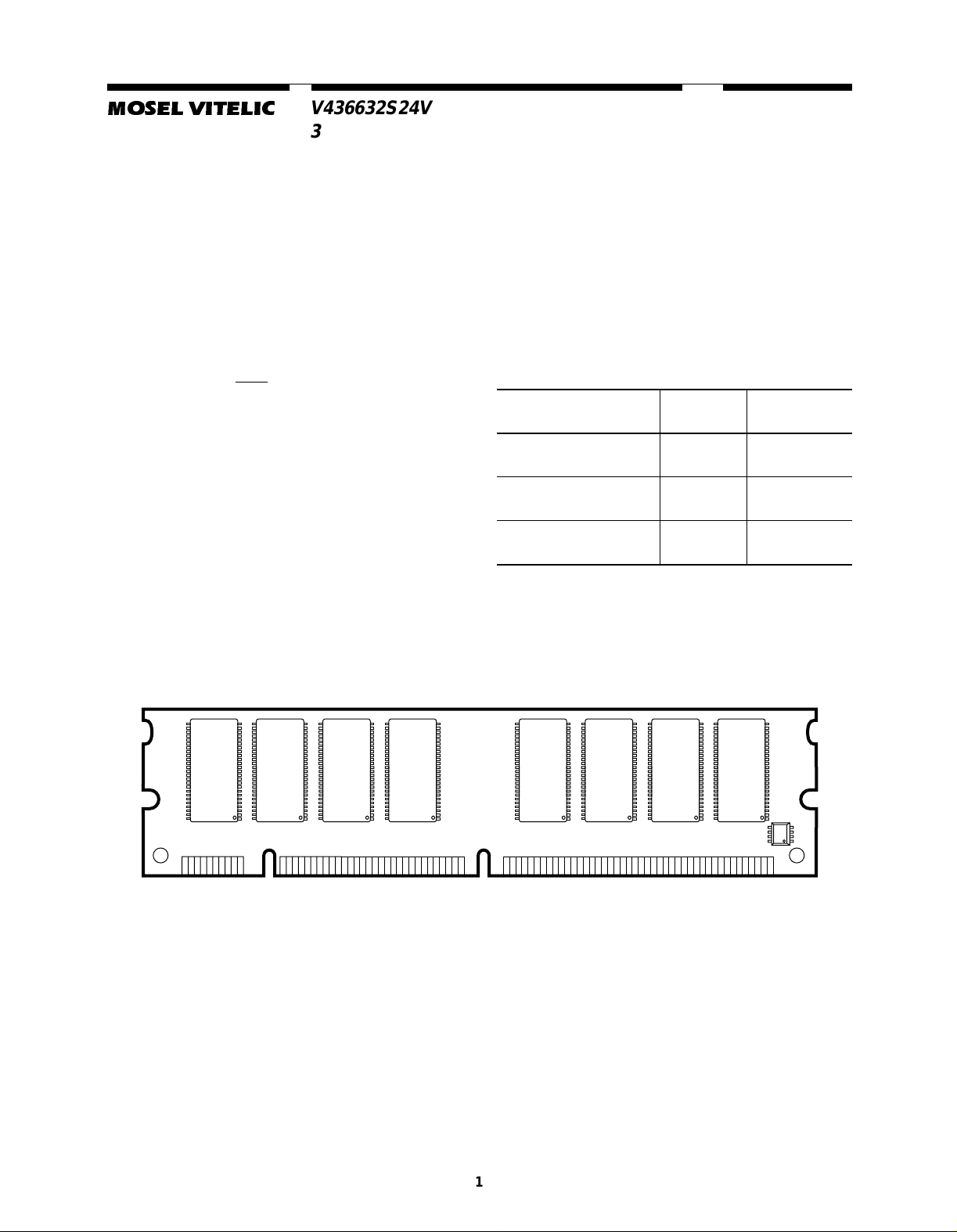
■ 168 Pin Unbuffered 33,554,432 x 64 bit
Oganization SDRAM Modules
■ Utilizes High Performance 32M x 8 SDRAM in
TSOPII-54 Packages
■ Fully PC Board Layout Compatible t o INTEL’S
Rev 1.0 Module Specification
■ Single +3.3V (± 0.3V) Power Sup ply
■ Programmable CAS
Wrap Sequence (Sequential & Interleave)
■ Auto Refresh (CBR) and Self Refresh
■ All Inputs, Outputs are LVTTL Compat ible
■ 8192 Refresh Cycles every 64 ms
■ Serial Presence Detect (SPD)
■
Latency, Burst Length, and
Description
The V436632S24V memory module is organized
33,554,432 x 64 bits in a 168 pin dual in line
memory modul e (DIMM). The 32M x 64 unbuffered
DIMM uses 8 Mosel-Vitelic 32M x 8 SDRAM. The
x64 m odules are ideal for use in high performance
computer systems where increased memory
density and fast access times are required.
Speed
Part Number
V436632S24VXTG-75PC -75PC, CL=2,3
V436632S24VXTG-75 -75, CL=3
V436632S24VXTG-10PC -10PC, CL=2,3
Grade Configuration
32Mx64
(133 MHz)
32Mx64
(133 MHz)
32Mx64
(100 MHz)
V436632S24V Rev. 1.0 January2002
1
Page 2
MOSEL VITELIC
V436632S24V
Pin Configurations ( Front Side/Back Side)
Pin Front Pin Front Pin Front Pin Back Pin Back Pin Back
10
11
12
13
14
15
16
17
18
19
20
21
22
23
24
25
26
27
28
1
2
3
4
5
6
7
8
9
VSS
I/O1
I/O2
I/O3
I/O4
VCC
I/O5
I/O6
I/O7
I/O8
I/O9
VSS
I/O10
I/O11
I/O12
I/O13
I/O14
VCC
I/O15
I/O16
CBO*
CB1*
VSS
NC
NC
VCC
WE
DQM0
29
30
31
32
33
34
35
36
37
38
39
40
41
42
43
44
45
46
47
48
49
50
51
52
53
54
55
56
DQM1
CS0
DU
VSS
A0
A2
A4
A6
A8
A10(AP)
BA1
VCC
VCC
CLK0
VSS
DU
CS2
DQM2
DQM3
DU
VCC
NC
NC
CB2*
CB3*
VSS
I/O17
I/O18
57
58
59
60
61
62
63
64
65
66
67
68
69
70
71
72
73
74
75
76
77
78
79
80
81
82
83
84
I/O19
I/O20
VCC
I/O21
NC
DU
CKE1
VSS
I/O22
I/O23
I/O24
VSS
I/O25
I/O26
I/O27
I/O28
VCC
I/O29
I/O30
I/O31
I/O32
VSS
CLK2
NC
WP
SDA
SCL
VCC
85
86
87
88
89
90
91
92
93
94
95
96
97
98
99
100
101
102
103
104
105
106
107
108
109
110
111
112
VSS
I/O33
I/O34
I/O35
I/O36
VCC
I/O37
I/O38
I/O39
I/O40
I/O41
VSS
I/O42
I/O43
I/O44
I/O45
I/O46
VCC
I/O47
I/O48
CB4*
CB5*
VSS
NC
NC
VCC
CAS
DQM4
113
114
115
116
117
118
119
120
121
122
123
124
125
126
127
128
129
130
131
132
133
134
135
136
137
138
139
140
DQM5
CS1
RAS
VSS
A1
A3
A5
A7
A9
BA0
A11
VCC
CLK1
A12
VSS
CKE0
CS3
DQM6
DQM7
DU
VCC
NC
NC
CB6*
CB7*
VSS
I/O49
I/O50
141
142
143
144
145
146
147
148
149
150
151
152
153
154
155
156
157
158
159
160
161
162
163
164
165
166
167
168
I/O51
I/O52
VCC
I/O53
NC
DU
NC
VSS
I/O54
I/O55
I/O56
VSS
I/O57
I/O58
I/O59
I/O60
VCC
I/O61
I/O62
I/O63
I/O64
VSS
CLK3
NC
SA0
SA1
SA2
VCC
Notes:
* T hese pins are not used in this module.
Pin Names
A0–A12 Address Inputs
I/O1–I/O64 Data Inputs/Outputs
RAS
CAS
WE
BA0, BA1 Bank Selects
, CKE1 Clock Enable
CKE0
0–CS3 Chip Select
CS
CLK0–CLK3 Clock Input
DQM0–DQM7 Data Mask
VCC Power (+3.3 Volts)
VSS Ground
SCL Clock for Presence Detect
Row Address Strobe
Column Address Strobe
Read/Write Input
SDA Serial Data OUT for Presence
Detect
SA0–A2 Serial Data IN for Presence
Detect
CB0–CB7 Check Bits(x72 Organization)
NC No Connection
DU Don’t Use
V436632S24V Rev. 1.0 January2002
2
Page 3
MOSEL VITELIC
Module Part Number Information
V436632S24V
MOSEL VITELIC
MANUFACTURED
Block Diagram
DQM0
I/O1–I/O8
DQM1
I/O9–I/O16
V 4 3 66 32 S 2 4 V X T G -XX
WE
CS0
SDRAM
10
10
3.3V
WIDTH
DEPTH
168 PIN Unbuffered
DIMM X8 COMPONENT
DQM
I/O1–I/O8
DQM
I/O1–I/O8
WE
WE
REFRESH
RATE 8K
CS
D0
CS
D1
LVTTL
4 BANKS
DQM4
I/O40–I/O33
DQM5
I/O48–I/O41
COMPONENT A=0.17um
REV LEVEL B=0.14um
10
10
LEAD FINISH
G=GOLD
COMPONENT
PACKAGE, T = TSOP
DQM
I/O1–I/O8
DQM
I/O1–I/O8
SPEED
75PC = PC133 CL3,2
75 = PC133 CL3
10PC = PC133 CL3,2
WE
CS
D4
WE
CS
D5
CS2
DQM2
I/O17–I/O24
DQM
I/O1–I/O8
10
DQM3
I/O25–I/O32
DQM
I/O1–I/O8
10
E2PROM SPD (256 WORD X 8 BITS)
SCL0
SA2
SA1
SA0
CLOCK WIRING
CLOCK INPUT LOAD
CLK0 5 SDRAM
CLK1 Termination
CLK2 4 SDRAMS +3.3pF Cap
CLK3 Termination
WE
WE
47K
SDA
WP
CS
D2
CS
D3
I/O49–I/O56
I/O57–I/O64
CKE0
RAS
CAS
WE
A(11:0)
BA0, BA1
V
CC
V
SS
DQM6
DQM7
10
10
WE
DQM
I/O1–I/O8
WE
DQM
I/O1–I/O8
CKE: SDRAM D0-D7
RAS: SDRAM D0-D7
CAS: SDRAM D0-D7
WE: SDRAM D0-D7
A(11:0): SDRAM D0-D7
BA0, BA1: SDRAM D0-D7
D0-D7
C0-C17
D0-D7
CS
D6
CS
D7
V436632S24V Rev. 1.0 January2002
3
Page 4
MOSEL VITELIC
V436632S24V
Serial Presence Detect Information
A serial presence det ec t storage device –
2
PROM – is assembled onto the module. Informa-
E
tion about the m odule configuration, spee d, etc. is
writtenintotheE
duction using a serial presence detect protocol (I
synchronous 2-wire bus)
2
PROM device during module pro-
SPD-Table
Byte
Number Function Described SPD Entry Value
0 Number of SPD bytes 128 80 80 80 1 Total bytes in Serial PD 256 08 08 08 2 Memory Type SDRAM 04 04 04 3 Number of Row Addresses (without BS bits) 13 0D 0D 0D 4 Number of ColumnAddresses (forx8SDRAM) 10 0A 0A 09 5 Number of DIMM Banks 1 01 01 01 6 Module Data Width 64 40 40 40 7 Module Data Width (continued) 0 00 00 00 8 Module Interface Levels LVTTL 01 01 01
9 SDRAM Cycle Time at CL=3 7.5 ns/10.0 ns 75 75 A0 10 SDRAM Access Time from Clock at CL=3 5.4 ns/6.0 ns 54 54 60 11 Dimm Config (Error Det/Corr.) none 00 00 00
-75PC -75 -10PC
Hex Value
2
C
12 Refresh Rate/Type Self-Refresh,7.8µs828282 13 SDRAM width, Primary x8 08 08 08 14 Error Checking SDRAM Data Width n/a / x8 00 00 00 15 MinimumClockDelayfromBacktoBackRan-
dom Column Address 16 Burst Length Supported 1, 2, 4, 8 0F 0F 0F 17 Number of SDRAM Banks 4 04 04 04 18 SupportedCAS 19 CS 20 WE 21 SDRAM DIMM Module Attributes Non Buffered/Non Reg. 00 00 00 22 SDRAM Device Attributes: General Vcc tol ± 10% 0E 0E 0E 23 Minimum ClockCycle TimeatCAS 24 Maximum Data Access Time from Clock for CL
25 Minimum Clock Cycle Time at CL = 1 Not Supported 00 00 00 26 Maximum Data Access Time from Clockat CL
27 Minimum Row Precharge Time 15 ns/20 ns 0F 14 14
Latencies CS Latency = 0 01 01 01
Latencies WL = 0 01 01 01
=2
=1
Latencies CL = 2, 3 06 06 06
Latency = 2 7.5 ns /10.0 ns 75 A0 A0
=1CLK 010101
t
ccd
5.4 ns/ 6.0 ns 54 60 60
Not Supported 00 00 00
28 Minimum Row Active to Row Active Delay t
29 Minimum RAS to CAS
V436632S24V Rev. 1.0 January2002
Delay t
RCD
RRD
14 ns/15 ns/16 ns 0E 0F 10
15 ns/20 ns 0F 14 14
4
Page 5

MOSEL VITELIC
SPD-Table
V436632S24V
Byte
Hex Value
Number Function Described SPD Entry Value
30 Minimum RAS Pulse Width t 31 Module Bank Density (Per Bank) 256 MByte 40 40 40 32 SDRAM Input Setup Time 1.5 ns/2.0 ns 15 15 20 33 SDRAMInputHold Time 0.8 ns/1.0 ns 08 08 10 34 SDRAM Data Input Setup Time 1.5 ns/2.0 ns 15 15 20 35 SDRAM Data Input Hold Time 0.8 ns/1.0 ns 08 08 10
36-61 Superset Information (May be used in Future) 00 00 00
62 SPDRevision Revision2/1.2 02 02 12 63 Checksum for Bytes 0 - 62 FD 42 B0 64 Manufacturer’s JEDEC ID Code Mosel Vitelic 40 40 40
65-71 Manufacturer’s JEDEC ID Code (cont.) 00 00 00
72 Manufacturing Location
73-90 ModulePartNumber(ASCII) V436632S24V 91-92 PCB Identification Code
93 Assembly Manufacturing Date (Year)
RAS
42 ns/45 ns 2A 2D 2D
-75PC -75 -10PC
94 Assembly Manufacturing Date (Week)
95-98 Assembly Serial Number
99-125 Reserved 00 00 00
126 Intel Specification for Frequency 64 64 64
127 Supported frequency
128+ Unused Storage Location 00 00 00
DC Characteristics
TA=0°Cto70°C; VSS=0V;VDD,V
Symbol Parameter
V
V
V
V
I
I
IH
IL
OH
OL
I(L)
O(L)
InputHighVoltage 2.0 VCC+0.3 V Input Low Voltage –0.5 0.8 V OutputHighVoltage (I OutputLowVoltage (I Input Leakage Current, any input
(0 V < V
Outputleakage current
(DQ is disabled, 0V < V
< 3.6 V, all other inputs = 0V)
IN
= –4.0 mA) 2.4 — V
OUT
=4.0mA) — 0.4 V
OUT
OUT<VCC
=3.3V± 0.3V
DDQ
)
Limit Values
–10 10 µA
–10 10 µA
UnitMin. Max.
V436632S24V Rev. 1.0 January2002
5
Page 6

MOSEL VITELIC
V436632S24V
Capacitance
TA=0°Cto70°C; VDD=3.3V± 0.3V, f = 1 MHz
Symbol Parameter Limit Values Unit
C
I1
C
I2
C
ICL
C
I3
C
I4
C
IO
C
SC
C
SD
Input Capacitance (A0 to A11, RAS,CAS,WE)85pF
Input Capacitance (CS0-CS3)30pF
Input Capacitance(CLK0-CLK3) 22 pF
Input Capacitance (CKE0, CKE1) 50 pF
Input Capacitance (DQM0-DQM7) 20 pF
Input/Output Capacitance (I/O1-I/064) 20 pF
Input Capacitance (SCL, SA0-2) 8 pF
Input/OutputCapacitance 18 pF
Absolute Maximum Ratings
Parameter Max. Units
VoltageonVDDSupplyRelativetoV VoltageonInputRelativetoV Operating Temperature 0to+70 °C Storage Temperature -55to125 °C Power Dissipation 6.5 W
SS
SS
-1 to 4.6 V
-1 to 4.6 V
V436632S24V Rev. 1.0 January2002
6
Page 7

MOSEL VITELIC
Standby and Refresh Currents
1
V436632S24V
TA=0°Cto70°C, VCC=3.3V± 0.3V
Symbol Parameter Test Conditions -75PC/75 -10PC Unit Note
ICC1 OperatingCurrent Burst length= 4, CL = 3
>=tRC(min),
t
RC
t
>=tCK(min), IO = 0 mA
CK
1840 1680 mA 1,2
2 Bank Interleave Operation
2P Precharged Standby Current in
I
CC
CKE< = VIL(max), tCK>=tCK(min) 16 16 mA
PowerDown Mode
2N Precharged Standby Current in
I
CC
Non-Power Down Mode
3P Active Standby Current in Power
I
CC
CKE> = VIH(min), tCK>=tCK(min), In-
360 280 mA CS =
put changed once in 3 cycles
CKE< = VIL(max), tCK>=tCK(min) 80 80 mA
Down Mode
3N Active Standby Current in Non-Pow-
I
CC
er Do wn Mode
4 Burst OperatingCurrent tRC= Infinite, CL = 3,
I
CC
CKE> = VIH(min), tCK>=tCK(min), Input changed one time
>=tCK(min), IO = 0 mA
t
CK
400 360 mA CS =
1360 960 mA 1, 2
2 Banks Activated
5 Auto Refresh Current tRC>= tRC(min) 1920 1760 mA 1,2
I
CC
6 Self Refresh Current CKE = <0,2V Standard 24 24 mA 1,2
I
CC
L-version 12 12
High
High
V436632S24V Rev. 1.0 January2002
7
Page 8

MOSEL VITELIC
V436632S24V
AC Characteristics
3,4
TA=0°to70°C; VSS=0V;VCC=3.3V± 0.3V , tT=1ns
# Symbol Parameter
Clock and Clock Enable
1tCKClock Cycle Time
CAS
Latency = 3
Latency = 2
CAS
2fCKSystem frequency
Latency = 3
CAS
CAS
Latency = 2
3t
4t
5t
6t
7t
8t
CKSP
9t
CKSR
10 t
Common Parameters
11 t
12 t
13 t
14 t
15 t
16 t
Refresh Cycle
17 t
SREX
18 t
Read Cycle
19 t
20 t
21 t
22 t
Write Cycle
23 t
24 t
25 t
Clock Ac ces s Time
AC
CAS
Latency = 3
Latency = 2
CAS
Clock High Pulse Width 2.5 – 2.5 – 3 – ns 6
CH
Clock Low Pulse Width 2.5 – 2.5 – 3 – ns 6
CL
Input Setup time 1.5 – 1.5 – 2 – ns 7
CS
InputHoldTime 0.8–0.8– 1 – ns7
CH
CKESetupTime(Powerdownmode) 2–2–2–ns8
CKESetupTime(SelfRefreshExit) 8–8–8–ns9
Transitiontime(riseandfall) 1–1–1–ns
T
RAS to CAS delay 15–20–20–ns
RCD
Cycle Time 70 120k 70 120k 70 120k ns
RC
ActiveCommandPeriod 42–45–45–ns
RAS
PrechargeTime 15–20–20–ns
RP
Bank to Bank Delay Time 14 – 15 – 20 – ns
RRD
CAS to CAS delay time (same bank) 1–1–1–CLK
CCD
Self Refresh Exit Time
RefreshPeriod(8192cycles) 64–64–64–ms8
REF
DataOutHoldTime 3–3–3–ns4
OH
DataOuttoLowImpedanceTime 0–0–0–ns
LZ
Data Out to High Impedance Time 3 7.5 3 7.5 3 8 ns 10
HZ
DQMDataOutDisableLatency 2–2–2–CLK
DQZ
DatainputtoPrecharge(writerecovery) 2–2–1–CLK
DPL
DataIntoActive/refresh 5–5–5–CLK11
DAL
DQMWriteMaskLatency 0–0–0–CLK
DQW
Limit Values
-75PC -75 -10PC
MIN MAX MIN MAX MIN MAX
7.5
7.5
10
–
133
–
133
–
–
5.4
6
–
7.5
10
10
10
10
–
133
–
100
–
–
5.4
6
–
10
–
–
–
–
100
100
6
6
–ns9
Unit Note
ns
ns
MHz
MHz
4,5
ns
ns
V436632S24V Rev. 1.0 January2002
8
Page 9

MOSEL VITELIC
V436632S24V
Notes:
1. The specified values are valid when addresses are changed no more than once during tCK(min.) and when No
Operation commands are registered on every r ising clock edge during t
bank.
(min). Values are shown per module
RC
2. The specified values are valid when data inputs (DQ’s) are stableduring t
RC
(min.).
3. All AC characteristics are shown for device level.
An initial pause of 100 µs is required after power-up,then a PrechargeAll Banks command must be given followed
by 8 Auto Refresh (CBR) cycles before the Mode Register Set Operation can begin.
4. AC timingtestshave V
time is measured between V
=0.4VandVIH= 2.4V with the timingreferenced to the 1.4Vcrossoverpoint.Thetransition
IL
and VIL. All AC measurements assume tT= 1 ns with t he AC output load circuit
IH
shown. Specific tac and toh parameters are measured with a 50 pF only, without any resistiveterminationand with
a input signal of 1V / ns edge rate between 0.8V and 2.0V.
+1.4V
50 Ohm
50 pF
50 pF
CLOCK
INPUT
OUTPUT
tSETUP tHOLD
tLZ
tAC
1.4V
tCL
tCH
tOH
t
tAC
T
2.4V
0.4V
1.4V
Z=50 Ohm
I/O
I/O
Measurement conditionsfor
tac and toh
tHZ
5. If clock rising time is longer than 1 ns, a time (t
/2 -0.5) ns has to be added to this parameter.
T
6. Rated at 1.5V
7. If t
is longer than 1 ns, a time (tT-1) ns has to be added to this parameter.
T
8. Any time that the refresh Period has been exceeded, a minimum of two Auto (CBR) Ref resh commands must be
given to “wake-up” the device.
9. Self Refresh Exit is a synchronous operation and begins on the 2nd positive clock edge after CKE returns high.
Self Refresh Exit is not complete until a time period equal to t
is satisfiedonce the Self Refresh Exit command
RC
is registered.
10. Referenced to the time which the output achieves the open circuit condition,not to output voltage levels.
11. t
V436632S24V Rev. 1.0 January2002
is equivalent to t
DAL
DPL+tRP
.
9
Page 10

MOSEL VITELIC
Package Diagram
L-DIM-168-30
SDRAM DIMM Module Pac kage
V436632S24V
All measurements in mm
133.37
17.80
127.35
11011 4041 84
3.0
63.68
85 94 95 124 125 168
6.35
3.125
Detail A
2.26
4.45
2.0
RADIUS
1.27 + 0.10
42.18
3.125
BA
6.35
2.0
3.175
Detail B
1.27
2.50
(2.54 max)
35.00
1.27 ± 0.100
4.0
D
1.0 ± 0.05
0.2 ± 0.15
Detail C
Tolerances: ± (0.13) unless otherwise specified.
V436632S24V Rev. 1.0 January2002
10
Page 11

MOSEL VITELIC
Label Information
V436632S24V
Module Density
MOSEL VITELIC
Part Number
Criteria of PC100 or PC133
(refer to MVI datasheet)
DIMM manufacture date code
UNBUFFERED DIMM
V436632S24VXXX-XX 256MB CLX
PC133U-XXX-542-A
XXXX-XXXXXXX
Assembly in Taiwan
PC133 54
CL= 3 or 2 (CLK)
= 3 or 2 (CLK)
t
RCD
= 3 or 2 (CLK)
t
RP
-XXXU
2
A
Gerber file Intel PC100 x8 Based
JEDEC SPD Revision 2
= 5.4 ns
t
AC
CAS Latency
2=CL2
3=CL3
V436632S24V Rev. 1.0 January2002
11
Page 12

MOSEL VITELIC
V436632S24V
WORLDWIDE OFFICES
U.S.A.
3910 NORTH FIRST STREET
SAN JOSE, CA 95134
PHONE: 408-433-6000
FAX: 408-433-0952
U.S. SALES OFFICES
WEST
3910 NORTH FIRST STREET
SAN JOSE, CA 95134
PHONE: 408-433-6000
FAX: 408-433-0952
TAIWAN
7F, NO. 102
MIN-CHUAN E. ROAD, SEC. 3
TAIPEI
PHONE: 886-2-2545-1213
FAX: 886-2-2545-1209
NO 19 LI HSIN ROAD
SCIENCE BASED IND. PARK
HSIN CHU, TAIWAN, R.O.C.
PHONE: 886-3-579-5888
FAX: 886-3-566-5888
CENTRAL / EAST
604 FIELDWOOD CIRCLE
RICHARDSON, TX 75081
PHONE: 214-352-3775
FAX: 214-904-9029
SINGAPORE
10 ANSON ROAD #23-13
INTERNATIONAL PLAZA
SINGAPORE 079903
PHONE: 65-3231801
FAX: 65-3237013
JAPAN
ONZE 1852 BUILDING 6F
2-14-6 SHINTOMI, CHUO-KU
TOKYO 104-0041
PHONE: 03-3537-1400
FAX: 03-3537-1402
UK & IRELAND
SUITE 50, GROVEWOOD
BUSINESS CENTRE
STRATHCLYDE BUSINESS
PARK
BELLSHILL, LANARKSHIRE,
SCOTLAND, ML4 3NQ
PHONE: 44-1698-748515
FAX: 44-1698-748516
GERMANY
(CONTINENTAL
EUROPE & ISRAEL)
BENZSTRASSE 32
71083 HERRENBERG
GERMANY
PHONE: +49 7032 2796-0
FAX: +49 7032 2796 22
© Copyright , MOSEL VITELIC Corp.
The information in this document is subject to change without
notice.
MOSEL VITELIC makes no commitment to update or keep current the information contained in t his document. N o part of this
document may be copied or reproduced in any form or by any
means without the prior written consent of MOSEL-VITELIC.
V436632S24V Rev. 1.0 January2002
Printedin U.S.A.
MOSEL VITELIC subjects its products to normal quality control
sampling techniques whichare intendedtoprovide an assurance
of high quality products suitable for usual commercial applications.MOSELVITELIC doesnot do testingappropriatetoprovide
100% product quality assurance and does not assume any liability for consequential or incidental arising from any use of its products. If such products are to be used in applications in which
personal injury might occur from failure, purchaser must do its
own quality assurance testing appropriate to such applications.
12
 Loading...