

Page 1

© 2000 V3 Semiconductor Corp. V380SDC_A0 Datasheet Rev 1.01 DS-SD01-0101
1
V380SDC A0 Datasheet
V380SDC High Performance SDRAM Controller
for 32-bit and 64-bit Embedded Processors
1.0 About the V380SDC
▼
Direct interface to these processors:
• AMD
®
AM29030/40™
• IBM
®
PowerPC 401™ Gx
• IDT
®
79RC32364™
• Intel
®
i960
®
Cx/Hx/Jx/Rx/Vx
• Motorola
®
M68040™ and 68K/ColdFire
®
• PowerPC™ 750/60x
▼
Up to 75 MHz local bus clock
▼
Up to 2 Kbytes of continuous burst access for
64-bit processors and 1 Kbyte for 32-bit
processors
▼
Zero-wait-state bursting
▼
Dynamic bus protocol switching
▼
User-customized processor bus interface
▼
Support for up to 2 Gbytes of (Enhanced)
SDRAM
▼
Compatible with PC66, PC100, PC133 SDRAM
▼
Supports a wide range of synchronous DRAMs,
from 16 Mbit to 256 Mbit
▼
Support for up to 4 single-bank or 2 dual-bank
industry standard 168-pin SDRAM DIMM(s) or
144-pin SO-DIMM(s)
▼
I
2
C EEPROM interface for Serial Presence
Detect (SPD) on DIMM
▼
Optional EEPROM initialization
▼
8-bit bus watch timer
▼
System heartbeat and watchdog timers
▼
Two 32-bit general purpose timers with pulsewidth modulation capability—useful for RTOS
▼
16-bytes of general purpose registers
▼
Designed to work with the EPC family of PCI
bridges from V3 Semiconductor
▼
3.3 V operation with 5 V tolerant inputs
▼
Industrial temperature range (
− 40°C to +85°C)
▼
Low-cost 100-pin PQFP package
DS-SD01-0101.fm Page 1 Monday, June 5, 2000 11:03 AM
Page 2
About the V380SDC
2
V380SDC_A0 Datasheet Rev 1.01 DS-SD01-0101 © 2000 V3 Semiconductor Corp.
The V380SDC High Performance SDRAM Controller provides all aspects of SDRAM control for high performance
embedded systems. The V380SDC enables system designers to replace many lower integration support components
with a single, high-integration device. This saves design time, board space, and manufacturing cost.
The V380SDC from V3 Semiconductor provides the necessary (Enhanced) SDRAM access protocol and bus timing
resources to work with the latest (E)SDRAM devices. The processor interface on the V380SDC implements the bus
protocol of many popular RISC CPUs (AM29030/40, PowerPC 401 Gx, IDT 79RC32364, i960 Cx/Hx/Jx/Rx/Vx,
M68040, 68K/ColdFire, PowerPC 750/60x). The V380SDC is also fully compatible with the EPC family of PCI
bridges available from V3 Semiconductor.
The
V380SDC
supports a total SDRAM memory subsystem size of up to 2 Gbytes. Standard memory devices from
16 Mbit to 256 Mbit are supported; 8-, 16-, 32-bit and 64-bit accesses are allowed. Four single-bank or two dualbank industry standard 168-pin PC SDRAM DIMM(s) or 144-pin SO-DIMM(s) with Serial Presence Detect (SPD)
are also supported.
The
V380SDC
provides an 8-bit bus watch timer to detect and recover from accesses to unpopulated memory
regions. Two on-chip, general purpose, 32-bit timers can be individually configured as a pulse width modulator or
they may be used in other modes such as retriggerable or one-shot.
The
V380SDC
is packaged in a low-cost 100-pin EIJA Plastic Quad Flat Pack (PQFP), and is available in 75 MHz
speed grade.
This document contains the product codes, pinout, package mechanical information, DC characteristics, and AC
characteristics for the V380SDC. Detailed functional information is contained in the User’s Manual.
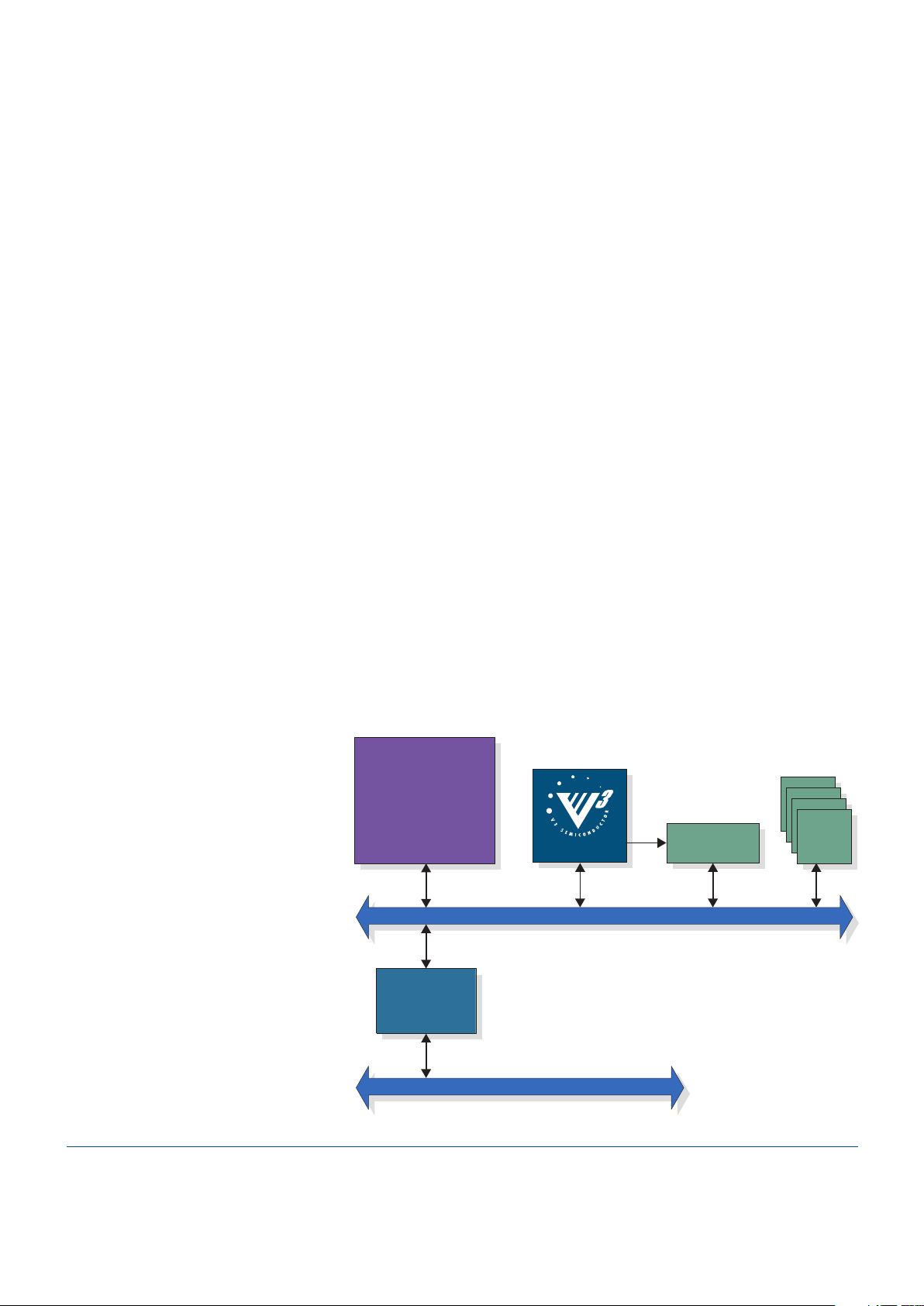
Figure 1: Example Application
Note:
V3 Semiconductor retains
the rights to change the
documentation, the
specifications, or device
functionality at any time
without notice. Contact V3
and verify that you have the
latest copy of all documents
before finalizing a design.
i960Cx/Hx/Jx/Rx/Vx,
PowerPC 401Gx,
IDT 79RC32364,
M68040/ColdFire/68K,
PowerPC 750, or
Am29030/40
Processor
V3
Local-to-PCI
Bridge
SDRAM
DIMM(s)
Flash
Local Bus
PCI Bus
V380SDC
DS-SD01-0101.fm Page 2 Monday, June 5, 2000 11:03 AM
Page 3
Product Codes
© 2000 V3 Semiconductor Corp. V380SDC_A0 Datasheet Rev 1.01 DS-SD01-0101
3
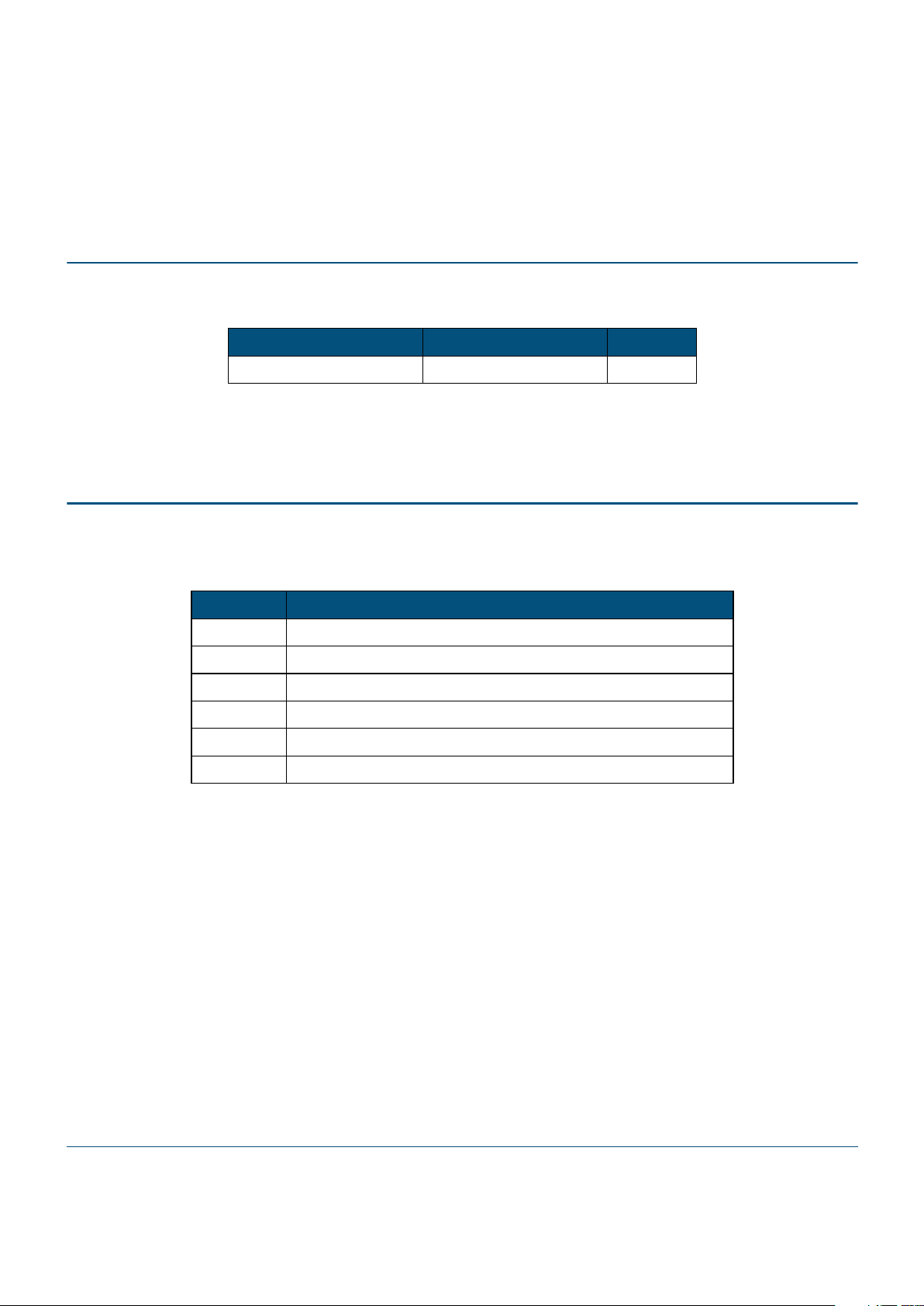
2.0 Product Codes
3.0 Pin Description
Table 2 lists the pin types found on the V380SDC; Table 3 describes the function of each pin.
Table 1: Product Code
Product Code
Package Frequency
V380SDC-75 REV A0 100-pin EIAJ PQFP 75 MHz
Table 2: Pin Types
Pin Type
Description
I/O
8
TTL I/O pin with 8 mA output drive.
I/O
D
TTL input with open drain output.
I TTL input only pin.
O
D
TTL open drain output.
O
8
TTL output pin with 8 mA output drive.
O
12
TTL output pin with 12 mA output drive.
DS-SD01-0101.fm Page 3 Monday, June 5, 2000 11:03 AM
Page 4
Pin Description
4
V380SDC_A0 Datasheet Rev 1.01 DS-SD01-0101 © 2000 V3 Semiconductor Corp.
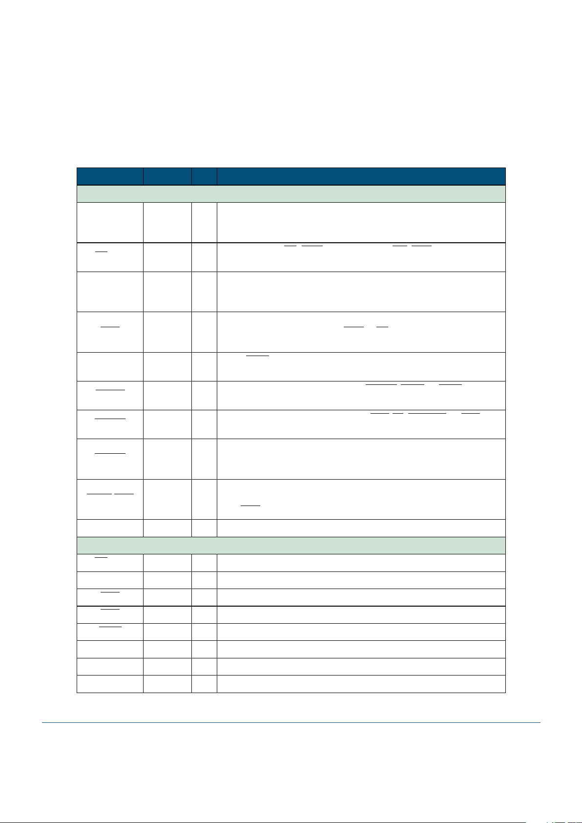
Table 3: Signal Descriptions
Signal
Type R
a
Description
Processor Bus Interface
A[31:2] I
Address Bus For demultiplexed processors, A[31:2] is used.
For multiplexed processors, only A[31:8] is used; A[2] is used as ALE
(Address Latch Enable) input.
BE[3:0] I
Byte Enables (BE
, BWE), Transfer Size (SIZ, TSIZ), or Address
(A[1:0]) are multiplexed on these pins depending on processor mode.
AD[7:0] I/O
8
Z
Address (Data) Bus For demultiplexed processors, AD[7:0] is used
as D[7:0]. For multiplexed processors, AD[7:0] is used as the
multiplexed address/data bus.
ADS
I
Address Strobe Asserted low to indicate the beginning of a bus
cycle: It can be interpreted as REQ or TS depending on processor
mode.
WNR I
Write/Read
It can be interpreted as RNW or RD depending on
processor mode.
BLAST
I
Burst Last It can be interpreted as BURST, TBST, or LAST
depending on processor mode.
READY I/O
8
Z
Data Ready It can be interpreted as RD
Y, TA, RDYRCV, or ACK
depending on processor mode.
ARTRY I
Address Retry for PPC750 processor. During reset, the state of the
pin along with the processor mode also determine the default value of
the SDC_REG_BASE register.
AACK/DEN I/O
8
Z
Address Acknowledge for PPC750 processor or Data Enable
output in other processor modes intended for buffer control.
This DEN
output is not to be connected to the processor.
TT[1:0] I
T ransfer Type
SDRAM Interface
CS[3:0] O
8
Z
SDRAM Chip Select
MA[14:0] O
12
Z
SDRAM Memory Address MA[14:13] are typically used for BA[1:0]
RAS
O
12
Z
SDRAM Row Address Strobe
CAS
O
12
Z
SDRAM Column Address Strobe
MWE
O
12
Z
SDRAM Memory Write Enable
DQM[7:0] O
8
Z
SDRAM Data Mask
IOC[3:0] I/O
8
Z
Multi-purpose I/O which can be configured for many functions
SDA I/O
D
Z
Serial EEPROM Data
DS-SD01-0101.fm Page 4 Monday, June 5, 2000 11:03 AM
Page 5

Pin Description
© 2000 V3 Semiconductor Corp. V380SDC_A0 Datasheet Rev 1.01 DS-SD01-0101
5
SCL O
D
Z
Serial EEPROM Clock
Clock and Reset
CLK I
Clock Input
RSTIN I
Reset Input Active low reset input used to initialize all internal
functions of the chip.
Power and Ground Signals
V
CC
—
POWER leads for external connection to a 3.3 V V
CC
board plane.
GND —
GROUND leads for external connection to a GND board plane.
a. R indicates state during reset.
Table 3: Signal Descriptions (cont’d)
Signal
Type R
a
Description
DS-SD01-0101.fm Page 5 Monday, June 5, 2000 11:03 AM
Page 6

Pin Description
Pinout
6
V380SDC_A0 Datasheet Rev 1.01 DS-SD01-0101 © 2000 V3 Semiconductor Corp.
3.1 Pinout
Table 4 lists the pins by pin number. Figure 2: Pinout for 100-pin EIAJ PQFP (top view) shows the pinout for the
100-pin EIAJ PQFP package and Figure 3: 100-pin EIAJ PQFP mechanical details shows the mechanical
dimensions of the package.
Table 4: Pin Assignments
PIN #
Signal PIN # Signal PIN # Signal PIN # Signal
1 RSTIN 26 A26 51 CS0 76 GND
2 A4 27 A27 52 CS2 77 MA1
3 A5 28 A28 53 MA14 78 MA0
4 A6 29 A29 54 MA13 79 RAS
5 A7 30 A30 55 MA12 80 CAS
6 A8 31 A31 56 DQM7 81 MWE
7 A9 32 AD0 57 DQM3 82 DQM4
8 A10 33 AD1 58 Vcc 83 GND
9 A11 34 AD2 59 GND 84 DQM0
10 A12 35 AD3 60 MA11 85 CS1
11 A13 36 AD4 61 MA10 86 CS3
12 A14 37 AD5 62 MA9 87 AACK/DEN
13 A15 38 AD6 63 MA8 88 SDA
14 A16 39 AD7 64 MA7 89 SCL
15 Vcc 40 Vcc 65 DQM6 90 Vcc
16 GND 41 GND 66 DQM2 91 GND
17 A17 42 CLK 67 GND 92 IOC0
18 A18 43 BE0 68 MA6 93 IOC1
19 A19 44 BE1 69 MA5 94 IOC2
20 A20 45 BE2 70 MA4 95 IOC3
21 A21 46 BE3 71 MA3 96 READY
22 A22 47 ADS 72 MA2 97 BLAST
23 A23 48 WNR 73 DQM5 98 A2
24 A24 49 TT0 74 DQM1 99 A3
25 A25 50 TT1 75 Vcc 100 ARTRY
DS-SD01-0101.fm Page 6 Monday, June 5, 2000 11:03 AM
Page 7

Pin Description
Pinout
© 2000 V3 Semiconductor Corp. V380SDC_A0 Datasheet Rev 1.01 DS-SD01-0101
7
Figure 2: Pinout for 100-pin EIAJ PQFP (top view)
RSTIN#
A4
A5
A6
A7
A8
A9
A10
A11
A12
A13
A14
A15
A16
Vcc
GND
A17
A18
A19
A20
A21
A22
A23
A24
A25
A26
A27
A28
A29
A30
A31
AD0
AD1
AD2
AD3
AD4
AD5
AD6
AD7
Vcc
GND
CLK
BE0#
BE1#
BE2#
BE3#
ADS#
WNR
TT0
TT1
CAS#
RAS#
MA0
MA1
GND
Vcc
DQM1
DQM5
MA2
MA3
MA4
MA5
MA6
GND
DQM2
DQM6
MA7
MA8
MA9
MA10
MA11
GND
Vcc
DQM3
DQM7
MA12
MA13
MA14
CS2#
CS0#
ARTRY#A3A2
BLAST#
READY#
IOC3
IOC2
IOC1
IOC0
GND
Vcc
SCL
SDA
AACK#/DEN#
CS3#
CS1#
DQM0
GND
DQM4
MWE#
80
100
51
31
81
50
1
30
V380SDC
DS-SD01-0101.fm Page 7 Monday, June 5, 2000 11:03 AM
Page 8

DC Specifications
Pinout
8
V380SDC_A0 Datasheet Rev 1.01 DS-SD01-0101 © 2000 V3 Semiconductor Corp.
Figure 3: 100-pin EIAJ PQFP mechanical details
4.0 DC Specifications
Table 5: Absolute Maximum Ratings
Symbol Parameter Value Units
V
CC
Supply voltage −0.3 to +3.6 V
V
IN
DC input voltage −0.3 to 6.0 V
T
STG
Storage temperature range −55 to +125 °C
DS-SD01-0101.fm Page 8 Monday, June 5, 2000 11:03 AM
Page 9

DC Specifications
Pinout
© 2000 V3 Semiconductor Corp. V380SDC_A0 Datasheet Rev 1.01 DS-SD01-0101 9
Table 6: Guaranteed Operating Conditions
Symbol Parameter Value Units
V
CC
Supply voltage 3.0 to 3.6 V
J
max
Maximum junction temperature 125 °C
Theta JaThermal resistance (Package) 75 °C/w
Theta JcThermal resistance (Junction-Case) 24 °C/w
T
A
Ambient temperature range −40 to +85 °C
Table 7: DC Operating Specifications (VCC = 3.3 V ± 0.3 V)
Symbol Parameter Condition Min Max Units
V
IH
Input high voltage 2.0 V
V
IL
Input low voltage 0.8 V
I
IH
Input high leakage current V
IN
= V
CC
−10 10 µA
I
IL
Input low leakage current V
IN
=GND −10 10 µA
V
OH
Output high voltage I
OUT
= -2, -8 mA 2.4 V
V
OL
Output low voltage I
OUT
= 2, 8 mA 0.4 V
I
OZL
Low level float input leakage V
OL
= GND −10 10 µA
I
OZH
High level float input leakage V
OH
= V
CC
−10 10 µA
ICC (max) Maximum supply current
L
CLK
= 75 MHz,
V
CC
= 3.3 V
60 mA
ICC (typ) Typical supply current
L
CLK
= 33 MHz,
V
CC
= 3.3 V
25 mA
ICC (stb) Stand-by current V
CC
= 3.3 V 2 mA
C
IO
Input and output capacitance 10 pF
DS-SD01-0101.fm Page 9 Monday, June 5, 2000 11:03 AM
Page 10

AC Specifications
Pinout
10 V380SDC_A0 Datasheet Rev 1.01 DS-SD01-0101 © 2000 V3 Semiconductor Corp.
5.0 AC Specifications
Figure 4: Clock and Synchronous Signals
Table 8: AC Test Conditions
Symbol Parameter Limits Units
V
CC
Supply voltage 3.3 volt operation 3.0 to 3.60 V
V
IN
Input low and high voltages 0.4 and 2.0 V
C
OUT
Capacitive load on output and I/O pins 50 pF
Table 9: Capacitive Derating for Output and I/O Pins
Output Drive Limit Supply voltage Derating
8 mA 3.3 volt +0.024 ns/pF for loads > 50pF
12 mA 3.3 volt +0.022 ns/pF for loads > 50pF
CLOCK
INPUT SETUP/HOLD
OUTPUT VALID
OUTPUT DRIVE
OUTPUT FLOAT
THTSU
TCL
TC
TCH
TCOZ
VALID
VALID
Tczo
TCOV
VALID
DS-SD01-0101.fm Page 10 Monday, June 5, 2000 11:03 AM
Page 11

AC Specifications
Pinout
© 2000 V3 Semiconductor Corp. V380SDC_A0 Datasheet Rev 1.01 DS-SD01-0101 11
Notes:
1 Valid when SYNC bit in the PB_IO_CFG register is set to ‘1’.
2 Valid when SYNC bit in the PB_IO_CFG register is set to ‘0’.
3 Used by the bus watch timer to monitor unclaimed access only.
4 Input through IOC1.
5 Except when in ColdFire MCF5102 mode.
6 Only in ColdFire MCF5102 mode.
7 For BE
changing with each datum in a burst write access only.
8 All IOC[3:0] input are synchronous except WAIT
.
Table 10: Timing Parameters for Vcc = 3.3 Volts ± 5%
75 MHz
# Symbol Description Notes Min Max Units
1TCCLK period 13.33 ns
2 T
CH
CLK high time 5.5 ns
3TCLCLK low time 5.5 ns
4a T
SU
Synchronous input setup
(except AACK, W AIT)
1, 8 3 ns
4b T
SU
Asynchronous input setup
(except AACK, W AIT, IOC[3:0])
2, 8 7 ns
4c T
SU
Input setup for AACK 3 4 ns
4d T
SU
Input setup for WAIT 413 ns
5 T
H
Synchronous input hold 5 1 ns
6a T
COV
CLK to output valid delay (except IOC[3:0]) 3 10 ns
6b T
COV
CLK to output valid delay (IOC[3:0] only) 3 12 ns
7T
COZ
CLK to high impedance delay 4 11 ns
8 T
AS
Address Setup to the trailing edge of ALE ns
9TAHAddress Hold from the trailing edge of ALE 2 ns
10 T
AH
Address Hold from the rising edge of CLK 6 5 ns
11 T
PDQ
Propogation Delay from BE to DQM 7 4 12 ns
Tc
2
------ -2–
DS-SD01-0101.fm Page 11 Monday, June 5, 2000 11:03 AM
Page 12

Getting Help from V3 Semiconductor
Serial EEPROM Port Timings
12 V380SDC_A0 Datasheet Rev 1.01 DS-SD01-0101 © 2000 V3 Semiconductor Corp.
5.1 Serial EEPROM Port Timings
The clock for the serial EEPROM interface is derived by dividing the processor bus clock. The waveforms generated
are shown in Figure 5.
Figure 5: Serial EEPROM Waveforms and Timings
6.0 Getting Help from V3 Semiconductor
If you need assistance with a technical question, please contact us. E-mail is the quickest and most efficient way to
get technical support from V3.
Corporate Office Sales Office
250 Consumers Road, Suite 901 2348G Walsh Avenue
Toronto, Ontario, Canada Santa Clara, California 95051
M2J 4V6 USA
Telephone: 1-877-283-7364 Telephone: 1-800-488-8410
(416) 497-8884 (408) 988-1050
Fax: (416) 497-1160 Fax: (408) 988-2601
E-mail: V3help@vcubed.com
Some technical support information is also posted on the V3 Web site. This is the source of the most up-to-date
documentation and is located at: http://www
.vcubed.com.
SCL
SDA
START CONDITION
STOP CONDITION
512 BUS
CLOCKS
256 BUS
CLOCKS
256 BUS
CLOCKS
DS-SD01-0101.fm Page 12 Monday, June 5, 2000 11:03 AM
Page 13

Revision History
Serial EEPROM Port Timings
© 2000 V3 Semiconductor Corp. V380SDC_A0 Datasheet Rev 1.01 DS-SD01-0101 13
7.0 Revision History
Table 11: Revision History
Revision
Number
Date Comments and Changes
0.8 08/99 First pre-silicon revision of preliminary datasheet.
0.9 12/99 Second revision of preliminary datasheet.
1.00 5/00 First release.
1.01 6/00
Add data to Table 7, “DC Operating Specifications (VCC = 3.3 V ± 0.3 V),” on
page 9.
DS-SD01-0101.fm Page 13 Monday, June 5, 2000 11:03 AM
 Loading...