

Page 1
Copyright © 1999, V3 Semiconductor Corp. V370PDC_A0 Data Sheet Rev 1.01 DS-PD01-0101
1
V370PDC
Rev. A0
High Performance PCI SDRAM Controller with
Integrated Peripheral Control Unit
V3 Semiconductor reser v es the right to change the specifications of this product without notice.
V370PDC is a trademark of V3 Se m iconductor Inc. All other trademarks are the proper ty of their respective owners.
V370PDC
SDRAM
and PROM
ISA
Conversion
Lo
g
ic
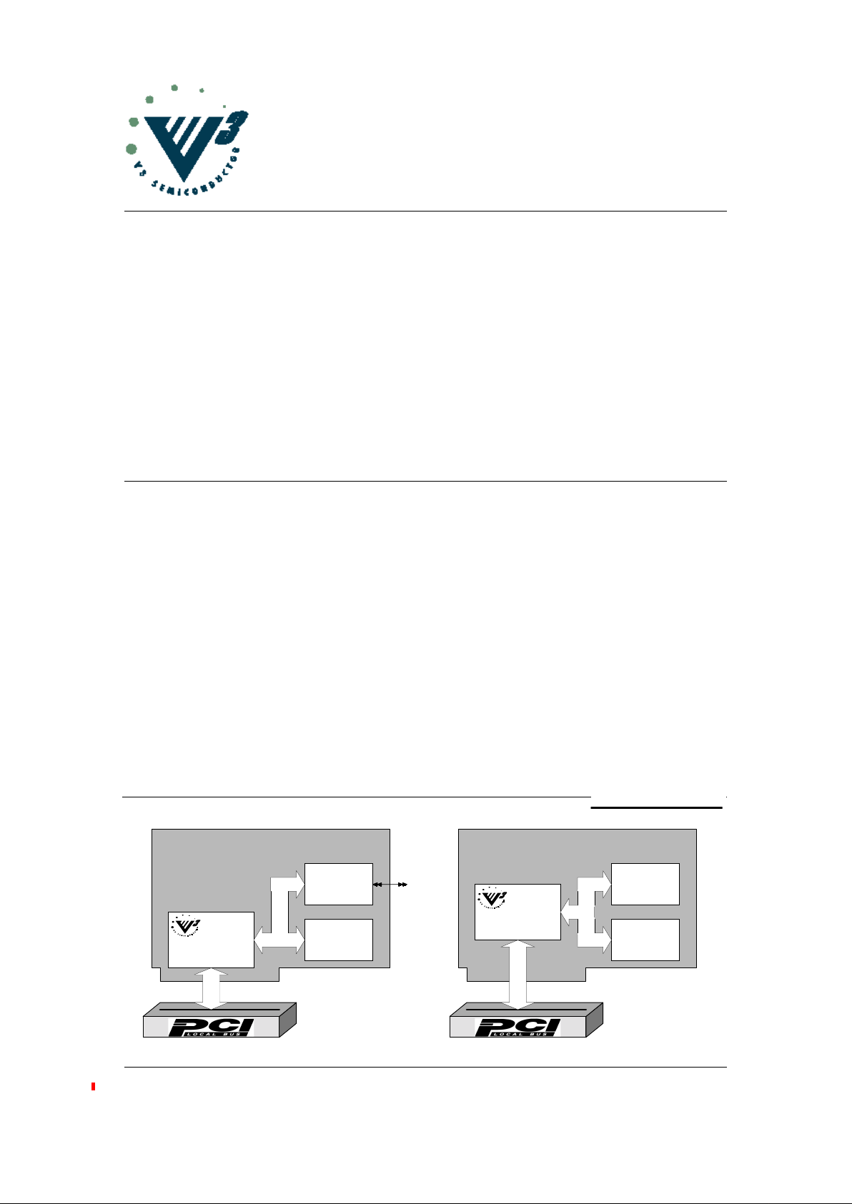
PCI-to-ISA Conversion
Application
V370PDC
SDRAM
SRAM/
FLASH
PCI Tar
g
et Onl
y
Application
• Fully compliant with PCI 2.2 specification target
interface
• Multiplexed or Non-multiplexe d 8-, 16-, or 32-bit
g
eneric peripheral bus interface
• Support up to 1 Gbyte of SDRAM
• Support up to 2 sin
g
le banks or 1 dual bank
industrial standard 168-p in PC SDRAM DIMM
• Support up to 1Kbyte of burst access from PCI
• Up to 5 pro
g
rammable chip select for peripheral
strobe
g
eneration
• Lar
g
e On-Chip FIFOs using V3’s unique
DYNAMIC BANDWIDTH ALLOCATION™
architecture
• Buffered PCI clock output
• Hot Swap Ready (PICMG™ Hot Swap
Specification)
• Implementation of PCI Bus Power M ana
g
ement
Interface Specification Version 1.0
• Initialization throu
g
h PCI or serial EEPROM
• Pro
g
rammable PCI and local interrupt
mana
g
ement
• Two 32-bit General Purpose Timers
• Up to 66 MHz local bus clock with asynchronous
PCI clock up to 33MHz
• 3.3V operation with 5V toleran t inputs
• Industrial Temperature Ran
g
e (-40C to +85C)
• Low cost 160-pin PQFP packa
g
e
The V370PDC PCI SDRAM C ontroll er simpl ifies t he
design of PCI based memory sub-systems. System
designers can replace many lower int egration supp ort
components with this single, hi gh-integ ration devi ce
saving design time, board area, and manufacturing
cost.
The V370PDC from V3 Semiconductor is a high
performance PCI SDRAM Controller with integrated
peripheral control unit operating at up to 66 MHz local
bus speed. It features multiple address translation
units from PCI which allow designers the freedom to
customize their local address space. Access latency of
slower peripherals are absorbed through the large OnChip FIFOs.
The peripheral bus provides low latency access to
SDRAM. The perip heral cont rol un it o n t he V370P DC
also performs address deco ding and chip-select
strobes generation for SRAM, PROM and other slow
peripherals. The peripheral bus can also be tri-stated
through a simple hand-shaking protocol to allow o ther
local bus masters control of the bus.
The SDRAM Controller connec ts the PCI bus thro ugh
on-chip FIFOs to SDRAM arrays of up to 1 Gbytes in
size. The fully programmable SDRAM controller also
supports the use of Enhanced SDRAM to achieve
even greater performance. Burst accesses of up to 1
Kbyte from PCI is supported.
The two general purpose 32-bit timers can be
individually configured as a pulse width modulator, or
used in other modes such as retriggerable or oneshot. Interrupts fo r a real time OS can be easily
generated by the system hear tbeat time r. A watchdog
timer is also provided for graceful recovery from
catastrophic program failures. Interrupt requests for all
on-chip peripheral s are managed b y the Interrupt
Control Unit. Additionally, off-chip interrupts can be
routed to the Interrupt Control Unit.
The V370PDC is packaged in a low-cost 160-pin EIJA
Plastic Quad Flat Pack (PQFP ), and is available in
66MHz speed grade.
TY PICAL AP PLI CATI ON
Page 2
V370PDC
2
V370PDC_A0 Data Sheet Rev 1.01 DS-PD01-0101 Copyright © 1999, V3 Semiconductor Inc.
This document contains the product codes, pinout, package mechanical information, DC
characteristics, and AC characteristics for the V370PDC. Detailed functional information is contained
in the User’s Manual.
V3 Semiconductor retains the rights to change documentation, sp ecifications, or devic e
functionality at any time without notice. Please verify that you have the latest copy of all
documents before finalizing a design.
1.0 Product Codes
2.0 Pin Description
Table 2 below lists the pin ty pes found on the V370PDC. Table 3 describes the function of ea ch pin on
the V370PDC.
Table 1: Product Codes
Product Code Package Frequency
V370PDC-66 REV A0 160-pin EIAJ PQFP 66MHz
Table 2: Pin Types
Pin T ype Description
PCI I PCI input only pin.
PCI O PCI output only pin.
PCI I/O PCI tri-state I/O pin.
PCI I/OD PCI input with open drain output.
I/O
8
TTL I/O pin with 8mA output drive.
I/OD TTL input with open drain output.
I TTL input only pin.
O
2
TTL output pin with 2mA output driv e.
O
8
TTL output pin with 8mA output driv e.
O
12
TTL output pin with 12mA output drive.
Page 3

V370PDC
Copyright © 1999, V3 Semiconductor Corp. V370PDC_A0 Data Sheet Rev 1.01 DS-PD01-0101
3
Table 3: Signal Descriptions
PCI Bus Interface
Signal Type R
a
Description
AD[31:0] PCI I/O Z Address and data, multiplexed on the same pins.
C/BE[3:0]
PCI I Bus Command and Byte Enables, multiplexed on the same pins.
PAR PCI I/O Z Parity represents even parity across AD[31:0] and C/BE[3:0].
FRAME PCI I
Cycle Frame indicates the beginning and burst length of an
access.
IRDY PCI I
Initiator Ready indi cates the init iating agen t’s (bus master’s) ability
to complete the current data phase of the transaction.
TRDY PCI O Z
Target Ready indicates the target agent’s (selected device’s) ability to complete the current data phase of the transaction.
STOP PCI O Z
Stop indicates the current target is requesting the master to stop
the current transaction (retry or disconnect).
DEVSEL PCI O Z
Device Select, when actively driven by a target, indicates the driving device has decoded its addr ess as the target of the current
access.
IDSEL PCI I
Initialization Device Select is used as a chip select during configuration read and write transactions. It must be driven high in order
to access the chip’s internal configuration space.
PERR PCI I/O Z
Parity Error is used to report data parity errors during all PCI
transactions except a Special Cycle.
SERR PCI I/OD Z
System Error is used to report address parity errors, data parity
errors on the Special Cycle command, or any other system error
where the result will be catastrophic.
PCLK PCI I PCLK provides timing for all transactions on the PCI bus.
SDRAM and Peripheral Bus Interfac e
Signal Type R Description
CLKIN I Local clock input
CLKOUT O
12
X Buffered PCI clock output
DCS[3:0] O
8
Z SDRAM Chip Select
MA[14:0] O
12
Z
SDRAM Memory Address (also, A[16:2] for peripheral access).
MA[14:13] are typically used for BA[1:0]
RAS O
12
Z SDRAM Row Address Strobe
Page 4
V370PDC
4
V370PDC_A0 Data Sheet Rev 1.01 DS-PD01-0101 Copyright © 1999, V3 Semiconductor Inc.
CAS O
12
Z SDRAM Column Address Strobe
MWE O
12
Z SDRAM Memory Write Enable
MAD[31:0] I/O
8
Z SDRAM and peripheral bus data
DQM[3:0] O
8
Z
SDRAM Data Mask (these act as MBE[3:0], A[1:0] for peripheral
access)
MARB_IN I
Peripheral bus arbitration input: Treated as bus request input
when V370PDC is the prima ry bus master. When V3 70PDC is the
secondary bus master, this input acts as bus grant.
MARB_OUT O
8
0
Peripheral bus arbitration output: Treated as bus grant output
when V370PDC is the prima ry bus master. When V3 70PDC is the
secondary bus master, this output acts bus request.
ALE O
8
Z
Address Latch Enable: used to latch the address on MAD[31:0]
during the address phase of a peripheral bus access.
ADS O
8
Z Asserted low to indicate the beginning of a bus cycle.
BLAST O
8
Z Burst last.
READY I Data ready.
WNR O
8
ZWrite/Read.
SDA I/OD Z Serial EEPROM Data
SCL O
2
Z Serial EEPROM Clock
IOC[11:0] I/O
8
Z Multi-purpose I/O that can be configured for many functions
INT[3:0] I/O
8
Z
General purpose inte rr upt inputs/outputs: ma y be used for eit her
PCI or local processor interrupts
Mode and Reset
Signal Type R Description
RSTIN
I
Reset Input: Active low reset input used to initialize all internal
functions of the chip.
RSTOUT
O
8
0
Reset Output: Driven active when the input reset is driven active.
Driven inactive when the RSTOUT bit in the system register is set.
The RSTOUT signal is synchronous to the rising edge of CLKIN.
CH
I
PCI Precharge Bias: This signal is driven low to activate the onchip precharg e bias for use in PICMG Hot Swap applications.
Non-Hot Swap applications should pull this signal high.
Table 3: Signal Descriptions (cont’d)
Page 5
V370PDC
Copyright © 1999, V3 Semiconductor Corp. V370PDC_A0 Data Sheet Rev 1.01 DS-PD01-0101
5
2.1 Pinout
Table 4 lists the pins by pin number. Figure 1 shows the pinout for the 160-pin EIAJ PQFP package
and Figure 2 shows the mechanical dimensions of the package
MODE I
MODE Input: selects mastership of V370PDC
:
0 = Secondary master
1 = Primary master
Power and Ground Signals
Signal Type R Description
V
CC
- POWER leads for external connection to a 3.3V VCC board plane.
GND - GROUND leads for external connection to a GND board plane.
NC - No connect.
a. R indicates state during reset.
Table 3: Signal Descriptions (cont’d)
Page 6

V370PDC
6
V370PDC_A0 Data Sheet Rev 1.01 DS-PD01-0101 Copyright © 1999, V3 Semiconductor Inc.
Table 4: Pin Assignments
PIN # Signal PIN # Signal PIN # Signal PIN # Signal
1RSTIN41 Vcc 81 Vcc 121 Vcc
2 PCLK42AD1482MAD9122MA5
3 GND 43 AD13 83 MA13 123 MAD27
4 Vcc 44 AD12 84 MAD10 124 MA4
5 NC 45AD1185MA12125MAD28
6CH46 AD10 86 MAD11 126 MA3
7 AD31 47 AD9 87 MA11 127 MAD29
8 AD30 48 AD8 88 MAD12 128 MAD30
9AD2949C_BE089 MA10 129 MAD31
10 AD28 50 MODE 90 GND 130 GND
11 AD27 51 GND 91 MAD13 131 MA2
12 AD26 52 AD7 92 IOC11 132 MA1
13 AD25 53 AD6 93 MAD14 133 MA0
14 AD24 54 AD5 94 IOC10 134 IOC3
15 GND 55 AD4 95 MAD15 135 IOC2
16 C_BE3 56 AD3 96 IOC9 136 READY
17 IDSEL 57 AD2 97 MAD16 137 MARB_OUT
18 AD23 58 AD1 98 IOC8 138 MARB_IN
19 AD22 59 AD0 99 MAD17 139 ADS
20 Vcc 60 Vcc 100 Vcc 140 Vcc
21 AD21 61 GND 101 GND 141 GND
22 AD20 62 MAD0 102 MA9 142 CLKIN
23 AD19 63 DCS0 103 MAD18 143 IOC1
24 AD18 64 MAD1 104 MA8 144 IOC0
25 AD17 65 DCS1 105 MAD19 145 DQM3
26 AD16 66 MAD2 106 MA7 146 DQM2
27 GND 67 DCS2 107 MAD20 147 DQM1
28 C_BE2 68 MAD3 108 MA6 148 DQM0
29 FRAME 69 DCS3 109 MAD21 149 BLAST
30 IRDY 70 MAD4 110 GND 150 WNR
31 TRDY
71 GND 11 1 MAD22 151 GND
32 DEVSEL
72 MAD5 112 IOC7 152 CLKOUT
33 STOP
73 MWE 113 MAD23 153 RSTOUT
34 PERR 74 MAD6 114 IOC6 154 ALE
35 SERR
75 CAS 115 MAD24 155 SDA
36 PAR 76 MAD7 116 IOC5 156 SCL
37 Vcc 77 RAS 117 MAD25 157 INT0
38 C_BE1 78 MAD8 1 18 IOC4 158 INT1
39 AD15 79 MA14 119 MAD26 159 INT2
40 GND 80 GND 120 GND 160 INT3
Page 7

V370PDC
Copyright © 1999, V3 Semiconductor Corp. V370PDC_A0 Data Sheet Rev 1.01 DS-PD01-0101
7
Figure 1: Pinout for 160-pin EIAJ PQFP (top view)
Page 8

V370PDC
8
V370PDC_A0 Data Sheet Rev 1.01 DS-PD01-0101 Copyright © 1999, V3 Semiconductor Inc.
Figure 2: 160-pin EIAJ PQFP mechanical details
Page 9

V370PDC
Copyright © 1999, V3 Semiconductor Corp. V370PDC_A0 Data Sheet Rev 1.01 DS-PD01-0101
9
3.0 DC Specifications
The DC specifications for the PCI bus signals match exactly those given in the PCI Specification, Rev.
2.2 Section 4.2.1.1. For more information on the PCI DC specifications, see the PCI Specific ation.
3.1 PCI Bus DC Specifications
Table 5: Absolute Maximum Rati ngs
Symbol Parameter Value Units
V
CC
Supply voltage -0.3 to +3.6 V
V
IN
DC input voltage -0.3 to 6.0 V
T
STG
Storage temperature range -55 to +125 °C
Table 6: Guaranteed Operating Conditions
Symbol Parameter Value Units
V
CC
Supply voltage 3.0 to 3.6 V
J
max
Maximum junction temperature 125 °C
Theta JaThermal resistance (Package) 41 to 46 °C/w
Theta JcThermal resistance (Junction-Case) 21 °C/w
T
A
Ambient temperature range -40 to +85 °C
Table 7: PCI Bus Signals DC Opera ti ng Spec if ica ti ons
Symbol Parameter Condition Min Max Units Notes
V
IH
Input high volt age 0.5V
CC
VCC + 0.5 V
V
IL
Input low voltage -0.5 0.3V
CC
V
I
IH
Input high leakage current 0.7V
CC
µ
A1
I
IL
Input low leakage current 0 < V
IN
< V
CC
+10
µ
A1
V
OH
Output high voltage I
OUT
= -500µA0.9V
CC
V
V
OL
Output low voltage I
OUT
= 1500µA0.1V
CC
V2
C
IN
Input pin cap acitance 10 pF 3
C
CLK
PCLK pin capacitance 5 12 pF
Page 10

V370PDC
10
V370PDC_A0 Data Sheet Rev 1.01 DS-PD01-0101 Copyright © 1999, V3 Semiconductor Inc.
Notes:
1. Input leakage currents include high impedance output leakage for all bi-directional buffers with tri-state outputs.
2. Signals without pull-up resistors have greater than 3mA low output current. Signals requiring pull resistors
have greater than 6mA output current. The latter include FRAME
, TRDY, IRDY, STOP, SERR, PERR.
3. Absolute maximum pin capacitance for a PCI unit is 10pF (except for CLK).
4. Lower capacitance on this input-only pin allows for non-resistive coupling to AD[xx].
3.2 Local Bus DC Specificati ons
C
IDSEL
IDSEL pin capacitan c e 8 pF 4
L
PIN
Pin inductanc e 20 nH
Table 8: Local Bus Signals DC Operating Specifications (VCC = 3.3V+ 0.3V)
Symbol Parameter Condition Min Max Units
V
IH
Input high voltage 2.0 V
V
IL
Input low voltage 0.8 V
I
IH
Input high leakage current V
IN
= V
CC
-10 10
µ
A
I
IL
Input low leakage current VIN=GND -10 10
µ
A
V
OH
Output high vo ltage I
OUT
= -2, -8, -12mA 2.4 V
V
OL
Output low voltage I
OUT
= 2, 8, 12mA 0.4 V
I
OZL
Low level float input leakage V
OL
= GND -10 10
µ
A
I
OZH
High level float input leakage V
OH
= V
CC
-10 10
µ
A
I
CC
(max) Maximum supply current PCLK=33MHz,
CLKIN=66MHz,
Vcc=3.6v,
all buses operating
70 mA
ICC (typ) Typical supply current 40 mA
C
IO
Input and output capacitance 10 pF
Table 7: PCI Bus Signals DC Opera ti ng Spec if ica ti ons
Symbol Parameter Condition Min Max Units Notes
Page 11

V370PDC
Copyright © 1999, V3 Semiconductor Corp. V370PDC_A0 Data Sheet Rev 1.01 DS-PD01-0101
11
3.3 AC Specifications
The AC specifications for the PCI bus signals match exactly those given in the PCI Specification, Rev.
2.1, Section 4.2.1.2. For more information on the PCI AC specifications, including the V/I curves for 5V
signalling, see section 4.2.1.2 of Rev 2.1 PCI Specification.
3.4 PCI Bus Timings
Table 9: PCI Bus Signals AC Opera ti ng Spec if ica ti ons
Symbol Parameter Condition Min Max Units Notes
I
OH(AC)
Switching
Current high
0V< V
OUT
≤ 0.3
V
CC
-12V
CC
mA
0.3VCC<V
OUT
<0.9V -17.1(VCC-V
OUT
)mA
0.7VCC<V
OUT<VCC
Equation C
(Test point) V
OUT =
0.7V
CC
-32V
CC
I
OL(AC)
Switching
Current low
VCC > V
OUT
>0.6
V
CC
16V
CC
mA
0.6VCC > V
OUT
>0.1
V
CC
26.7V
CC
mA
(Test point) V
OUT
=
0.18
V
CC
38V
CC
mA
I
CL
Low clamp
current
-3V<VIN<-1V -25+(VIN+1)/0.015 mA
t
R
Unloaded
output rise
time
0.2VCC to 0.6V
CC
14V/ns
t
F
Unloaded
output fall
time
0.6V to 0.2V 1 4 V/ns
Page 12

V370PDC
12
V370PDC_A0 Data Sheet Rev 1.01 DS-PD01-0101 Copyright © 1999, V3 Semiconductor Inc.
3.5 Local Bus Timings
Figure 3: Clock and Synchronous Signals
:
Table 10: Local Bus AC Test Conditions
Symbol Parameter Limits Units
V
CC
Supply voltage 3.3 volt op er ati on 3.0 to 3.60 V
V
IN
Input low and high voltages 0.4 and 2.0 V
C
OUT
Capacitive loa d on output and I/O pins 50 pF
Table 11: Capacitive Derating for Output and I/O Pins
Output Drive Limit Supply voltage Derating
8mA 3.3 volt 0.01 9 ns /pF for loads > 50pF
12mA 3.3 volt 0.017 ns/pF for loads > 50pF
Page 13

V370PDC
Copyright © 1999, V3 Semiconductor Corp. V370PDC_A0 Data Sheet Rev 1.01 DS-PD01-0101
13
Notes:
1. Applies only to READY
pin when i960_RDY bit in LB_BUS_CFG register is set to ’1’.
Table 12: Local Bus Timing Parameters for Vcc =3.3 Volts +/- 5%
66MHz
# Symbol Description Notes Min Max Units
1T
C
CLKIN period 15 ns
2TCHCLKIN high time 5.5 ns
3TCLCLKIN low time 5.5 ns
4TSUSynchronous input setup 3 ns
4a T
SU
Asynchronous input setup (READY)17 ns
5THSynchronous input hold 1 ns
6T
COV
CLKIN to output valid delay 3 11 ns
7T
CZO
CLKIN to output driving delay 3 11 ns
8T
COZ
CLKIN to high impedance delay 4 12 ns
9T
ALE
ALE Pulse Width TCH+0.5 TCH+1 ns
10 T
CLH
CLKIN rising to ALE rising 2 10 ns
11 T
AH
CLKIN falling to ALE falling 2 10 ns
Table 13: PCI Bus Timing Parameters for Vcc = 3.3 Volts +/- 10%
# Symbol Description Notes Min Max Units
1T
C
PCLK period 30 ns
2T
SU
Synchronous input setup to PCLK 1 7 ns
3T
H
Synchronous input hold from PCLK 0 ns
4T
COV
PCLK to output valid delay 2 3 11 ns
5T
CZO
PCLK to output driving delay 4 11 ns
6T
COZ
PCLK to high impedance delay 5 18 ns
7T
RST
Reset period when PRST used as input 16·T
C
Page 14

V370PDC
14
V370PDC_A0 Data Sheet Rev 1.01 DS-PD01-0101 Copyright © 1999, V3 Semiconductor Inc.
3.6 Serial EEPROM Port TImings
The clock for the serial EEPROM interface is derived by dividing the PCI bus clock. T he waveforms
generated ar e shown in Figure 4.
Figure 4: Serial EEPROM Waveforms and Timings
4.0 Revision History
USA:
2348G Walsh Avenue
Santa Clara, CA 95051
Phone: (408)988-1050 Fax: (408)988-2601
Toll Free: (800)488-8410 (Canada and U.S. only)
World Wide Web: http://www.vcubed.com
Table 14: Revision History
Revision
Number
Date Comments and Changes
0.8 01/99 First pre-silicon revision of preliminary data sheet.
0.9 03/99
Update Figure 2: Mechanical Drawing;
Update T able 8: Local Bus Signals DC Operating Specifications;
Update Table 10: Local Bus AC Test Conditions;
Update Table 12: Local Bus Signals AC Operating Specifications.
1.0 03/99 Initial Rel ease.
1.1 06/00 Updated TBA para meters
SCL
SDA
START CONDITION
STOP CONDITION
512 PCI BUS
CLOCKS
256 PCI BUS
CLOCKS
256 PCI BUS
CLOCKS
 Loading...