

Page 1
Datasheet
Copyright © 1999 V3 Semiconductor Inc. V320USC B1 Datasheet Rev 1.02 DS-UC01-0102
1
V3 Semiconductor Corp.
2348G W alsh Avenue
Santa Clara, CA 95051
Phone (408) 988-1050, Fax (408) 988-2601
Toll Free (800) 488-8410 (US and Canada)
http://www.vcubed.com
• Glueless interface between popular MIPS™ and
SuperH™ processors and the standard 32-bit PCI bus
• Fully compliant with PCI 2.2 specification
• Configurable for primary master, bus master, or target
operation
• SDRAM controller with support for Enhanced SDRAM
• Up to 1 Kbyte burst access to (E)SDRAM from PCI,
32 bytes from local processor (MIPS mode)
• 640 bytes of on-chip FIFO storage with
Dynamic
Bandwidth Allocation™ architecture
• On-the-fly byte order (endian) conversion
• I
2
O Ready™ ATU and messaging unit
• Programmable chip select / peripheral device
strobe generation
• Hot Swap Ready (PICMG™ Hot Swap Specification 2.1)
• Implementation of PCI Bus Pow er Management Interf ace
Specification V ersion 1.0
• 3.3V operation with 5V tolerant inputs
• 208-pin PQFP package
• Up to 75 MHz local bus clock with separate
asynchronous PCI clock up to 50 MHz
• Two 32-bit timers
• Initialization through local processor, PCI or serial
EEPROM
Typical Application
V320USC Universal System Controller
PCI System Controller for 32-Bit MIPS™ and SuperH™ System Interface
DS-UC01-0102.fm Page 1 Wednesday, June 30, 1999 7:30 PM
Page 2

2
V320USC B1 Datasheet Rev 1.02 DS-UC01-0102 Copyright © 1999 V3 Semiconductor Inc.
V320USC Datasheet
Introduction
1.0 Introduction
The V320USC Universal System Controller simplifies the design of systems based on MIPS and SuperH microprocessors
by replacing many lower integration support components with a single, high-integration device. This saves design time,
board area, and manufacturing cost.
The I
2
O Ready V320USC from V3 Semiconductor is a high performance PCI bridge with integrated SDRAM controller for
MIPS processors operating at up to 75 MHz bus speed. It features address translation capabilities and large on-chip
buffers. A separate peripheral bus provides low latency access to SDRAM. The peripheral controller on the V320USC also
performs address decoding and chip-select strobes generation for SRAM, PROM and other slow peripherals.
The integrated SDRAM Controller connects the processor as well as the PCI bus through on-chip FIFOs to SDRAM arrays
of up to 1 Gbytes in size. The fully programmable SDRAM controller also supports the use of Enhanced SDRAM to achieve
even greater performance. Burst accesses of up to 1 Kbytes from PCI and 32 bytes from the MIPS
processor are
supported.
The two general purpose 32-bit timers can be individually configured as a pulse width modulator, or used in other modes
such as retriggerable or one-shot. The bus watch timer (MIPS mode) prevents system hangs during accesses to
undecoded regions. Interrupts for a real time OS can be easily generated by the system heartbeat timer. A watchdog timer
is also provided for graceful recovery from catastrophic program failures. Interrupt requests for all on-chip peripherals are
managed by the Interrupt Control Unit. Additionally, off-chip interrupts can be routed to the Interrupt Control Unit.
The V320USC is packaged in a low-cost 208-pin EIJA Plastic Quad Flat Pack (PQFP), and is available in 75 MHz speed
grade (MIPS mode), 66 MHz (SH mode).
This document contains the product codes, pinout, package mechanical information, DC characteristics, and AC
characteristics for the V320USC. Detailed functional information is contained in the User’s Manual.
1.1 Listing of Figures
Figure 1: Pinout for 208-pin EIAJ PQFP in MIPS Mode (top view) . . . . . . . . . . . . . . . . . . . . . . . . . . 13
Figure 2: Pinout for 208-pin EIAJ PQFP in SH3/4 Mode (top view) . . . . . . . . . . . . . . . . . . . . . . . . . . 14
Figure 3: 208-pin EIAJ PQFP mechanical details . . . . . . . . . . . . . . . . . . . . . . . . . . . . . . . . . . . . . . . 15
Figure 4: Clock and Synchronous Signals . . . . . . . . . . . . . . . . . . . . . . . . . . . . . . . . . . . . . . . . . . . . . 19
Figure 5: ALE Timing . . . . . . . . . . . . . . . . . . . . . . . . . . . . . . . . . . . . . . . . . . . . . . . . . . . . . . . . . . . . . 19
Figure 6: Serial EEPROM Waveforms and Timings . . . . . . . . . . . . . . . . . . . . . . . . . . . . . . . . . . . . . 21
1.2 Listing of Tables
Table 1: Product Code . . . . . . . . . . . . . . . . . . . . . . . . . . . . . . . . . . . . . . . . . . . . . . . . . . . . . . . . . . . . . 3
Table 2: Pin Types . . . . . . . . . . . . . . . . . . . . . . . . . . . . . . . . . . . . . . . . . . . . . . . . . . . . . . . . . . . . . . . . 3
Table 3: Signal Description—PCI Bus Interface . . . . . . . . . . . . . . . . . . . . . . . . . . . . . . . . . . . . . . . . . 4
Table 4: Signal Description—Local Bus Interface, MIPS™ Mode . . . . . . . . . . . . . . . . . . . . . . . . . . . . 5
Table 5: Signal Description—Local Bus Interface, SH3/4 Mode . . . . . . . . . . . . . . . . . . . . . . . . . . . . . 5
Table 6: Signal Description—DRAM and Peripheral Bus Interface . . . . . . . . . . . . . . . . . . . . . . . . . . . 6
Table 7: Signal Description—Mode and Reset . . . . . . . . . . . . . . . . . . . . . . . . . . . . . . . . . . . . . . . . . . 7
Table 8: Signal Description—Power and Ground Signals . . . . . . . . . . . . . . . . . . . . . . . . . . . . . . . . . . 8
Table 9: Signal Description—Power and Ground Signals . . . . . . . . . . . . . . . . . . . . . . . . . . . . . . . . . . 8
Table 10: Pin Assignments for MIPS™ Mode . . . . . . . . . . . . . . . . . . . . . . . . . . . . . . . . . . . . . . . . . . . 8
DS-UC01-0102.fm Page 2 Wednesday, June 30, 1999 7:30 PM
Page 3
V320USC Datasheet
Product Code
Copyright © 1999 V3 Semiconductor Inc. V320USC B1 Datasheet Rev 1.02 DS-UC01-0102
3
Table 11: Pin Assignments for SH3/4 Mode . . . . . . . . . . . . . . . . . . . . . . . . . . . . . . . . . . . . . . . . . . . 10
Table 12: Absolute Maximum Ratings . . . . . . . . . . . . . . . . . . . . . . . . . . . . . . . . . . . . . . . . . . . . . . . . 15
Table 13: Guaranteed Operating Conditions . . . . . . . . . . . . . . . . . . . . . . . . . . . . . . . . . . . . . . . . . . . 16
Table 14: DC Operating Conditions . . . . . . . . . . . . . . . . . . . . . . . . . . . . . . . . . . . . . . . . . . . . . . . . . . 16
Table 15: PCI Bus Signals DC Operating Specifications . . . . . . . . . . . . . . . . . . . . . . . . . . . . . . . . . . 16
Table 16: Local Bus/M Bus Signals DC Operating Specifications (VCC = 3.3V+ 0.3V) . . . . . . . . . . 17
Table 17: PCI Bus Signals AC Operating Specifications . . . . . . . . . . . . . . . . . . . . . . . . . . . . . . . . . . 17
Table 18: Local and M Bus AC Test Conditions . . . . . . . . . . . . . . . . . . . . . . . . . . . . . . . . . . . . . . . . 18
Table 19: M Bus AC Test Conditions . . . . . . . . . . . . . . . . . . . . . . . . . . . . . . . . . . . . . . . . . . . . . . . . . 18
Table 20: Capacitive Derating for Output and I/O Pins . . . . . . . . . . . . . . . . . . . . . . . . . . . . . . . . . . . 19
Table 21: Local Bus/M-Bus Timing Parameters for Vcc =3.3 Volts +/- 5% . . . . . . . . . . . . . . . . . . . . 19
Table 22: PCI Bus Timing Parameters for Vcc = 3.3 Volts +/- 10% . . . . . . . . . . . . . . . . . . . . . . . . . . 20
Table 23: Revision History . . . . . . . . . . . . . . . . . . . . . . . . . . . . . . . . . . . . . . . . . . . . . . . . . . . . . . . . . 21
V3 Semiconductor retains the rights to change documentation, specifications, or
device functionality at any time without notice. Please verify that you have the latest copy
of all documents before finalizing a design.
2.0 Product Code
3.0 Pin Description
Table 2 lists the pin types found on the V320USC.
Table 1: Product Code
Product Code
Processors Package Frequency
V320USC-75 REV B1
MIPS (32-bit bus), SH3,
SH4 (32-bit bus)
208-pin EIAJ PQFP
75MHz
(66 MHz SH)
Table 2: Pin Types
Pin Type
Description
PCI I PCI input only pin.
PCI O PCI output only pin.
PCI I/O PCI tri-state I/O pin.
PCI I/OD PCI input with open drain output.
DS-UC01-0102.fm Page 3 Wednesday, June 30, 1999 7:30 PM
Page 4
4
V320USC B1 Datasheet Rev 1.02 DS-UC01-0102 Copyright © 1999 V3 Semiconductor Inc.
V320USC Datasheet
Pin Description
3.1 Signal Description
The following tables describe the function of each pin on the V320USC.
I/O
2
,
I/O
8
,
I/O
12
TTL I/O pins with 2/8/12 mA drive
I TTL input only pin.
O
2
,
O
8
,
O
12
TTL output pins with 2/8/12 mA drive
Table 3: Signal Description—PCI Bus Interface
Signal
Type R
a
Description
AD[31:0] PCI I/O Z Address and data, multiplexed on the same pins.
C/BE[3:0]
PCI I/O Z Bus Command and Byte Enables, multiplexed on the same pins.
PAR PCI I/O Z Parity represents even parity across AD[31:0] and C/BE[3:0].
FRAME PCI I/O Z
Cycle Frame indicates the beginning and burst length of an
access.
IRDY PCI I/O Z
Initiator Ready indicates the initiating agent’s (bus master’s) ability
to complete the current data phase of the transaction.
TRDY PCI I/O Z
Target Ready indicates the target agent’s (selected device’s)
ability to complete the current data phase of the transaction.
STOP PCI I/O Z
Stop indicates the current target is requesting the master to stop
the current transaction (retry or disconnect).
DEVSEL PCI I/O Z
Device Select, when actively driven by a target, indicates the
driving device has decoded its address as the target of the current
access. As an input to the initiator, DEVSEL indicates whether
any device on the bus has been selected.
IDSEL PCI I
Initialization Device Select is used as a chip select during
configuration read and write transactions. It must be driven high in
order to access the chip’s internal configuration space.
PERR
PCI I/O Z
Parity Error is used to report data parity errors during all PCI
transactions except a Special Cycle.
Table 2: Pin Types
Pin Type
Description
DS-UC01-0102.fm Page 4 Wednesday, June 30, 1999 7:30 PM
Page 5
V320USC Datasheet
Pin Description
Copyright © 1999 V3 Semiconductor Inc. V320USC B1 Datasheet Rev 1.02 DS-UC01-0102
5
SERR
PCI I/OD Z
System Error is used to report address parity errors, data parity
errors on the Special Cycle command, or any other system error
where the result will be catastrophic.
REQ PCI O Z
Request indicates to the arbiter that this agent requests use of the
bus.
GNT
PCI I
Grant indicates to the agent that access to the bus has been
granted.
PCLK PCI I PCLK provides timing for all transactions on the PCI bus.
a. R indicates state during reset.
Table 4: Signal Description—Local Bus Interface, MIPS™ Mode
Signal
Type R Description
SYSAD[31:0] I/O Z System Address / Data (multiplexed)
SYSCMD[8:0] I/O Z
System Command / data identifier. When MODE0 = ‘0’,
SYSCMD[8:5] should be pulled high.
VALIDIN O
8
Z
Valid command or data from external agent. This signal should
have an external pull-up resistor.
V
ALIDOUT I Valid command or data from MIPS™
RELEASE I Release the system interface to slave state
WRRDY O
8
Z Write Ready: this signal should have an external pull-up resistor.
LCLK I Local clock
Table 5: Signal Description—Local Bus Interface, SH3/4 Mode
Signal Type R Description
A[31:26]/
CS[5:0]
I/O
8
I
Z
Upper System Address
A[25:0] I/O
8
Z Lower System Address
D[31:0] I/O
8
Z Data Bus
RD/WR
I/O
8
Z Read/not Write. This is also referred to as MWE
for SDRAM
Table 3: Signal Description—PCI Bus Interface
Signal
Type R
a
Description
DS-UC01-0102.fm Page 5 Wednesday, June 30, 1999 7:30 PM
Page 6
6
V320USC B1 Datasheet Rev 1.02 DS-UC01-0102 Copyright © 1999 V3 Semiconductor Inc.
V320USC Datasheet
Pin Description
BS
I Bus Cycle Start
WAIT/RDY O
8
Z Bus Wait
RBE_EN
a
I
Enable Read Byte Enables: When active (‘0’), PCI byte lane
enables are derived from RBE
[3:0] for a local-to-PCI read access.
RBE
[3:0]
b
I
Read Byte Enables: provides the byte enable pattern for local-toPCI read access when RBE_EN
is active. Byte enables for writes
are derived from the DQM
[3:0] signals.
BREQ
O
8
Z
Bus Request Output: indicates that the V320USC wants to
perform a bus cycle on the local bus
BA
CK I
Bus Acknowledge: asserted to allow the V320USC to take
ownership of the local bus.
BREQ_IN
c
I
Bus Request Input: assertion of this input will cause the V320USC
to give up ownership of the local bus at the end of the current
burst/single cycle so that a higher priority master can take
ownership. Typically connected to IRQ_OUT
.
LCLK I
Local clock. This would be connected to either CKIO on the
processor or a clock driver which provides a clock with the same
phase relationship as CKIO. See V3 Reference Designs for
further details.
a.Not available in revision B0 silicon
b.Not available in revision B0 silicon
c.Not available in revision B0 silicon
Table 6: Signal Description—DRAM and Peripheral Bus Interface
Signal Type R Description
MA[14:0] O
12
Z
SDRAM Memory Address (also, A[16:2] for peripheral access).
MA[14:13] are typically used for BA[1:0]
DCS
[3:0] O
8
Z
SDRAM Chip Select. This should be connected to the CS inputs
of SDRAM chips or DIMM devices.
DQM[3:0] I/O
8
Z
SDRAM Data Mask (these act as MBE[3:0], A[1:0] for peripheral
access)
RAS
O
12
Z SDRAM Row Address Strobe
CAS
O
12
Z SDRAM Column Address Strobe
MWE
O
12
Z SDRAM Memory Write Enable
Table 5: Signal Description—Local Bus Interface, SH3/4 Mode
Signal
Type R Description
DS-UC01-0102.fm Page 6 Wednesday, June 30, 1999 7:30 PM
Page 7
V320USC Datasheet
Pin Description
Copyright © 1999 V3 Semiconductor Inc. V320USC B1 Datasheet Rev 1.02 DS-UC01-0102
7
MAD[31:0] I/O
8
Z
SDRAM and peripheral bus data. MAD[31:0] is known as D[31:0]
when in SH3/4 mode.
SDA I/OD
2
Z Serial EEPROM Data
SCL O
2
Z Serial EEPROM Clock
IOC[11:0] I/O
8
Z Multi-purpose I/O that can be configured for many functions
INT
[3:0] PCI I/OD Z
General purpose interrupt inputs/outputs: may be used for either
PCI or local processor interrupts
Table 7: Signal Description—Mode and Reset
Signal
Type R Description
RSTIN I
Reset Input: Active low reset input used to initialize all internal
functions of the chip.
RSTOUT O
8
0
Reset Output: Driven activ e when the input reset is driv en activ e.
Driven inactive when the RST OUT bit in the system register is set.
The RST
OUT signal is synchronous to the rising edge of LCLK.
CH I
PCI Precharge Bias: This signal is driven low to activate the onchip precharge bias for use in PICMG Hot Swap applications.
Non-Hot Swap applications should pull this signal high.
MODE2:1
MODE0
I/O
8
I
Z
MODE Input: selects the CPU mode
:
‘H’ - Tie High with a weak pull up of 4.7–10K Ω
‘L’ - Tie Low with a weak pull down of 4.7–10K Ω
Table 6: Signal Description—DRAM and Peripheral Bus Interface
Signal
Type R Description
MODE
2 1 0 Description
Pin 55 Pin 54 Pin 202
SYSCMD7 SYSCMD8 ‘H’ MIPS with 9 bit SYSCMD
‘H’ ‘H’ ‘L’ MIPS with 5 bit SYSCMD
‘H’ ‘L’ ‘L’ SH3
‘L’ ‘L’ ‘L’ SH4
others reserved
DS-UC01-0102.fm Page 7 Wednesday, June 30, 1999 7:30 PM
Page 8

8
V320USC B1 Datasheet Rev 1.02 DS-UC01-0102 Copyright © 1999 V3 Semiconductor Inc.
V320USC Datasheet
Pin Description
3.2 Pinout
T able 10 lists the pins by pin number. Figure 1 and Figure 2 show the pinouts for the 208-pin EIAJ PQFP package. Figure
3: 208-pin EIAJ PQFP mechanical details shows the mechanical dimensions of the package.
Table 8: Signal Description—Power and Ground Signals
Signal
Type R Description
V
CC
- POWER leads for external connection to a 3.3V V
CC
board plane.
GND - GROUND leads for external connection to a GND board plane.
NC - No connect.
’H’ - Tie High with a weak pull up of 4.7K-10K
Table 9: Signal Description—Power and Ground Signals
Signal
Type R Description
V
CC
- POWER leads for external connection to a 3.3V V
CC
board plane.
GND - GROUND leads for external connection to a GND board plane.
NC - No connect.
’H’ - Tie High with a weak pull up of 4.7K-10K
Table 10: Pin Assignments for MIPS™ Mode
PIN #
Signal PIN # Signal PIN # Signal PIN # Signal
1V
CC
53 Vcc
105 Vcc 157 Vcc
2 AD29 54 SYSCMD8 106 SYSAD0 158 CAS
3 AD28 55 SYSCMD7 107 MAD31 159 IOC11
4 AD27 56 SYSCMD6 108 SYSAD31 160 RAS
5 AD26 57 SYSCMD5 109 MAD30 161 IOC10
6 AD25 58 SYSCMD4 110 SYSAD30 162 MA13
7 AD24 59 SYSCMD3 111 MAD29 163 IOC9
8 C/BE3 60 SYSCMD2 112 SYSAD29 164 MA12
DS-UC01-0102.fm Page 8 Wednesday, June 30, 1999 7:30 PM
Page 9

V320USC Datasheet
Pin Description
Copyright © 1999 V3 Semiconductor Inc. V320USC B1 Datasheet Rev 1.02 DS-UC01-0102
9
9 GND 61 SYSCMD1 113 MAD28 165 MA11
10 IDSEL 62 SYSCMD0 114 GND 166 GND
11 AD23 63 RELEASE 115 SYSAD28 167 INT3
12 AD22 64 VALIDOUT 116 MAD27 168 MA10
13 AD21 65 GND 117 SYSAD27 169 MA9
14 AD20 66 VALIDIN 118 MAD26 170 IOC8
15 AD19 67 WRRDY 119 SYSAD26 171 MA8
16 AD18 68 MAD15 120 MAD25 172 IOC7
17 AD17 69 SYSAD15 121 SYSAD25 173 MA6
18 GND 70 MAD14 122 MAD24 174 IOC6
19 Vcc 71 SYSAD14 123 Vcc 175 GND
20 AD16 72 MAD13 124 GND 176 Vcc
21 C/BE2 73 SYSAD13 125 SYSAD24 177 MA7
22 FRAME 74 MAD12 126 MAD23 178 IOC5
23 IRDY 75 GND 127 SYSAD23 179 MA5
24 TRDY 76 Vcc 128 MAD22 180 IOC4
25 DEVSEL 77 SYSAD12 129 SYSAD22 181 MA4
26 STOP 78 MAD11 130 MAD21 182 IOC3
27 GND 79 SYSAD11 131 SYSAD21 183 MA2
28 PERR 80 MAD10 132 MAD20 184 ’H’
29 SERR 81 SYSAD10 133 SYSAD20 185 GND
30 PAR 82 MAD9 134 CH 186 IOC2
31 C/BE1 83 SYSAD9 135 LCLK 187 MA3
32 AD15 84 MAD8 136 GND 188 DQM1
33 AD14 85 GND 137 Vcc 189 MA1
34 AD13 86 SYSAD8 138 MAD19 190 DQM0
Table 10: Pin Assignments for MIPS™ Mode (cont’d)
PIN #
Signal PIN # Signal PIN # Signal PIN # Signal
DS-UC01-0102.fm Page 9 Wednesday, June 30, 1999 7:30 PM
Page 10

10
V320USC B1 Datasheet Rev 1.02 DS-UC01-0102 Copyright © 1999 V3 Semiconductor Inc.
V320USC Datasheet
Pin Description
35 GND
87 MAD7 139 SYSAD19 191 MA0
36 Vcc 88 SYSAD7 140 MAD18 192 IOC1
37 AD12 89 MAD6 141 SYSAD18 193 GND
38 AD11 90 SYSAD6 142 MAD17 194 Vcc
39 AD10 91 MAD5 143 SYSAD17 195 INT2
40 AD9 92 SYSAD5 144 MAD16 196 SCL
41 AD8 93 MAD4 145 MA14 197 SDA
42 C/BE0 94 GND 146 GND 198 INT1
43 AD7 95 Vcc 147 SYSAD16 199 INT0
44 GND 96 SYSAD4 148 IOC0 200 RSTOUT
45 AD6 97 MAD3 149 DQM3 201 RSTIN
46 AD5 98 SYSAD3 150 DQM2 202 MODE0
47 AD4 99 MAD2 151 DCS3 203 PCLK
48 AD3 100 SYSAD2 152 DCS2 204 GNT
49 AD2 101 MAD1 153 DCS1 205 REQ
50 AD1 102 SYSAD1 154 DCS0 206 AD31
51 AD0 103 MAD0 155 MWE 207 AD30
52 GND 104 GND 156 GND 208 GND
Table 11: Pin Assignments for SH3/4 Mode
PIN #
Signal PIN # Signal PIN # Signal PIN # Signal
1 Vcc
53 Vcc 105 Vcc 157 Vcc
2 AD29 54 MODE1 106 A0 158 CAS
3 AD28 55 MODE2 107 D31 159 IOC11
4 AD27 56 'H' 108 A31/CS5 160 RAS
5 AD26 57 BREQ_IN 109 D30 161 IOC10
Table 10: Pin Assignments for MIPS™ Mode (cont’d)
PIN #
Signal PIN # Signal PIN # Signal PIN # Signal
DS-UC01-0102.fm Page 10 Wednesday, June 30, 1999 7:30 PM
Page 11

V320USC Datasheet
Pin Description
Copyright © 1999 V3 Semiconductor Inc. V320USC B1 Datasheet Rev 1.02 DS-UC01-0102
11
6 AD25 58 RBE_EN 110 A30/CS4 162 A15
7 AD24 59 RBE3 111 D29 163 IOC9
8 C/BE3 60 RBE2 112 A29/CS3 164 A14
9 GND 61 RBE1 113 D28 165 A13
10 IDSEL 62 RBE0 114 GND 166 GND
11 AD23 63 BACK 115 A28/CS2 167 INT3
12 AD22 64 BS 116 D27 168 A12
13 AD21 65 GND 117 A27/CS1 169 A11
14 AD20 66 WAIT/RDY 118 D26 170 IOC8
15 AD19 67 BREQ 119 A26/CS0 171 A10
16 AD18 68 D15 120 D25 172 IOC7
17 AD17 69 NC 121 A25 173 A8
18 GND 70 D14 122 D24 174 IOC6
19 Vcc 71 NC 123 Vcc 175 GND
20 AD16 72 D13 124 GND 176 Vcc
21 C/BE2 73 NC 125 A24 177 A9
22 FRAME 74 D12 126 D23 178 IOC5
23 IRDY 75 GND 127 A23 179 A7
24 TRDY 76 Vcc 128 D22 180 IOC4
25 DEVSEL 77 NC 129 A22 181 A6
26 STOP 78 D11 130 D21 182 IOC3
27 GND 79 NC 131 A21 183 A4
28 PERR 80 D10 132 D20 184 ’H’
29 SERR 81 NC 133 A20 185 GND
30 PAR 82 D9 134 CH 186 IOC2
31 C/BE1 83 NC 135 LCLK 187 A5
Table 11: Pin Assignments for SH3/4 Mode (cont’d)
PIN #
Signal PIN # Signal PIN # Signal PIN # Signal
DS-UC01-0102.fm Page 11 Wednesday, June 30, 1999 7:30 PM
Page 12

12
V320USC B1 Datasheet Rev 1.02 DS-UC01-0102 Copyright © 1999 V3 Semiconductor Inc.
V320USC Datasheet
Pin Description
32 AD15
84 D8 136 GND 188 DQMLU/WE1
33 AD14 85 GND 137 Vcc 189 A3
34 AD13 86 NC 138 D19 190 DQMLL/WE0
35 GND 87 D7 139 A19 191 A2
36 Vcc 88 NC 140 D18 192 IOC1
37 AD12 89 D6 141 A18 193 GND
38 AD11 90 NC 142 D17 194 Vcc
39 AD10 91 D5 143 A17 195 INT2
40 AD9 92 NC 144 D16 196 SCL
41 AD8 93 D4 145 A16 197 SDA
42 C/BE0 94 GND 146 GND 198 INT1
43 AD7 95 Vcc 147 NC 199 INT0
44 GND 96 NC 148 IOC0 200 RSTOUT
45 AD6 97 D3 149
DQMUU/
WE3
201 RSTIN
46 AD5 98 NC 150 DQMUL/WE2 202 MODE0
47 AD4 99 D2 151 DCS3 203 PCLK
48 AD3 100 NC 152 DCS2 204 GNT
49 AD2 101 D1 153 DCS1 205 REQ
50 AD1 102 A1 154 DCS0 206 AD31
51 AD0 103 D0 155 RD/WR 207 AD30
52 GND 104 GND 156 GND 208 GND
Table 11: Pin Assignments for SH3/4 Mode (cont’d)
PIN #
Signal PIN # Signal PIN # Signal PIN # Signal
DS-UC01-0102.fm Page 12 Wednesday, June 30, 1999 7:30 PM
Page 13

V320USC Datasheet
Pin Description
Copyright © 1999 V3 Semiconductor Inc. V320USC B1 Datasheet Rev 1.02 DS-UC01-0102
13
Figure 1: Pinout for 208-pin EIAJ PQFP in MIPS Mode (top view)
Vcc
CAS#
IOC11
RAS#
IOC10
MA13
IOC9
MA12
MA11
GND
INT3#
MA10
MA9
IOC8
MA8
IOC7
MA6
IOC6
GND
Vcc
MA7
IOC5
MA5
IOC4
MA4
IOC3
MA2
'H'
GND
IOC2
MA3
DQM1#
MA1
DQM0#
MA0
IOC1
GND
Vcc
INT2#
SCL
SDA
INT1#
INT0#
RSTOUT#
RSTIN#
MODE
PCLK
GNT#
REQ#
AD31
AD30
GND
Vcc
AD29
AD28
AD27
AD26
AD25
AD24
C_BE3#
GND
IDSEL
AD23
AD22
AD21
AD20
AD19
AD18
AD17
GND
Vcc
AD16
C_BE2#
FRAME#
IRDY#
TRDY#
DEVSEL#
STOP#
GND
PERR#
SERR#
PAR
C_BE1#
AD15
AD14
AD13
GND
Vcc
AD12
AD11
AD10
AD9
AD8
C_BE0#
AD7
GND
AD6
AD5
AD4
AD3
AD2
AD1
AD0
GND
GND
MAD0
SYSAD1
MAD1
SYSAD2
MAD2
SYSAD3
MAD3
SYSAD4
Vcc
GND
MAD4
SYSAD5
MAD5
SYSAD6
MAD6
SYSAD7
MAD7
SYSAD8
GND
MAD8
SYSAD9
MAD9
SYSAD10
MAD10
SYSAD11
MAD11
SYSAD12
Vcc
GND
MAD12
SYSAD13
MAD13
SYSAD14
MAD14
SYSAD15
MAD15
WRRDY#
VALIDIN#
GND
VALIDOUT#
RELEASE#
SYSCMD0
SYSCMD1
SYSCMD2
SYSCMD3
SYSCMD4
SYSCMD5
SYSCMD6
SYSCMD7
SYSCMD8
Vcc
GND
MWE#
SDRAM_CS0#
SDRAM_CS1#
SDRAM_CS2#
SDRAM_CS3#
DQM2#
DQM3#
IOC0
SYSAD16
GND
MA14
MAD16
SYSAD17
MAD17
SYSAD18
MAD18
SYSAD19
MAD19
Vcc
GND
LCLK
CH#
SYSAD20
MAD20
SYSAD21
MAD21
SYSAD22
MAD22
SYSAD23
MAD23
SYSAD24
GND
Vcc
MAD24
SYSAD25
MAD25
SYSAD26
MAD26
SYSAD27
MAD27
SYSAD28
GND
MAD28
SYSAD29
MAD29
SYSAD30
MAD30
SYSAD31
MAD31
SYSAD0
Vcc
104
53
156
1
105
52
157
208
V320USC
MIPS Mode
DS-UC01-0102.fm Page 13 Wednesday, June 30, 1999 7:30 PM
Page 14

14 V320USC B1 Datasheet Rev 1.02 DS-UC01-0102 Copyright © 1999 V3 Semiconductor Inc.
V320USC Datasheet
Pin Description
Figure 2: Pinout for 208-pin EIAJ PQFP in SH3/4 Mode (top view)
Vcc
CAS#
IOC11
RAS#
IOC10
A15
IOC9
A14
A13
GND
INT3#
A12
A11
IOC8
A10
IOC7
A8
IOC6
GND
Vcc
A9
IOC5
A7
IOC4
A6
IOC3
A4
'H'
GND
IOC2
A5
DQMLU#/WE1#
A3
DQMLL#/WE0#
A2
IOC1
GND
Vcc
INT2#
SCL
SDA
INT1#
INT0#
RSTOUT#
RSTIN#
MODE0
PCLK
GNT#
REQ#
AD31
AD30
GND
Vcc
AD29
AD28
AD27
AD26
AD25
AD24
C_BE3#
GND
IDSEL
AD23
AD22
AD21
AD20
AD19
AD18
AD17
GND
Vcc
AD16
C_BE2#
FRAME#
IRDY#
TRDY#
DEVSEL#
STOP#
GND
PERR#
SERR#
PAR
C_BE1#
AD15
AD14
AD13
GND
Vcc
AD12
AD11
AD10
AD9
AD8
C_BE0#
AD7
GND
AD6
AD5
AD4
AD3
AD2
AD1
AD0
GND
GND
D0
A1
D1
NC
D2
NC
D3
NC
Vcc
GND
D4
NC
D5
NC
D6
NC
D7
NC
GND
D8
NC
D9
NC
D10
NC
D11
NC
Vcc
GND
D12
NC
D13
NC
D14
NC
D15
BREQ#
WAIT#/RDY#
GND
BS#
BACK#
RBE0#
RBE1#
RBE2#
RBE3#
RBE_EN#
BREQ_IN#
H
MODE2
MODE1
Vcc
GND
RD/WR#
DCS0#
DCS1#
DCS2#
DCS3#
DQMUL#/WE2#
DQMUU#/WE3#
IOC0NCGND
A16
D16
A17
D17
A18
D18
A19
D19
Vcc
GND
LCLK
CH#
A20
D20
A21
D21
A22
D22
A23
D23
A24
GND
Vcc
D24
A25
D25
A26/CS0#
D26
A27/CS1#
D27
A28/CS2#
GND
D28
A29/CS3#
D29
A30/CS4#
D30
CS5#
D31A0Vcc
104
53
156
1
105
52
157
208
V320USC
SH3/4 Mode
DS-UC01-0102.fm Page 14 Wednesday, June 30, 1999 7:30 PM
Page 15

V320USC Datasheet
DC Specifications
Copyright © 1999 V3 Semiconductor Inc. V320USC B1 Datasheet Rev 1.02 DS-UC01-0102 15
Figure 3: 208-pin EIAJ PQFP mechanical details
4.0 DC Specifications
The DC specifications for the PCI bus signals match exactly those given in the PCI Specification, Rev. 2.2 Section 4.2.1.1.
For more information on the PCI DC specifications, see the PCI Specification.
Table 12: Absolute Maximum Ratings
Symbol Parameter Value Units
V
CC
Supply voltage -0.3 to +3.6 V
V
IN
DC input voltage -0.3 to 6.0 V
T
STG
Storage temperature range -55 to +125 ˚C
DS-UC01-0102.fm Page 15 Wednesday, June 30, 1999 7:30 PM
Page 16

16 V320USC B1 Datasheet Rev 1.02 DS-UC01-0102 Copyright © 1999 V3 Semiconductor Inc.
V320USC Datasheet
DC Specifications
4.1 PCI Bus DC Specifications
Notes:
1. Input leakage currents include high impedance output leakage for all bi-directional buffers with tri-state outputs.
2. Signals without pull-up resistors have greater than 3mA low output current. Signals requiring pull resistors have greater than 6mA
output current. The latter include FRAME
, TRDY, IRDY, STOP, SERR, PERR.
3. Absolute maximum pin capacitance for a PCI unit is 10pF (except for CLK).
4. Lower capacitance on this input-only pin allows for non-resistive coupling to AD[xx].
Table 13: Guaranteed Operating Conditions
Symbol Parameter Value Units
V
CC
Supply voltage 3.0 to 3.6 V
Theta Ja Thermal resistance 40 to 45 ˚C/w
T
A
Ambient temperature range -40 to +85 ˚C
Table 14: DC Operating Conditions
Symbol Parameter Max Units Condition
ICC(max) Maximum supply current 110 mA
PCLK=33MHz, LCLK=66MHz,
Vcc=3.6V, all buses operating
ICC(typ) Typical supply current 80 mA
Table 15: PCI Bus Signals DC Operating Specifications
Symbol Parameter Condition Min Max Units Notes
V
IH
Input high voltage 0.5V
CC
VCC + 0.5 V
V
IL
Input low voltage -0.5 0.3V
CC
V
I
IH
Input high leakage current 0.7V
CC
µA1
I
IL
Input low leakage current 0 < V
IN
< V
CC
+10 µA1
V
OH
Output high voltage I
OUT
= -500µA 0.9V
CC
V
V
OL
Output low voltage I
OUT
= 1500µA 0.1V
CC
V2
C
IN
Input pin capacitance 10 pF 3
C
CLK
PCLK pin capacitance 5 12 pF
C
IDSEL
IDSEL pin capacitance 8 pF 4
L
PIN
Pin inductance 20 nH
DS-UC01-0102.fm Page 16 Wednesday, June 30, 1999 7:30 PM
Page 17

V320USC Datasheet
AC Specifications
Copyright © 1999 V3 Semiconductor Inc. V320USC B1 Datasheet Rev 1.02 DS-UC01-0102 17
4.2 Local Bus DC Specifications
5.0 AC Specifications
The AC specifications for the PCI bus signals match exactly those given in the PCI Specification, Rev. 2.1, Section 4.2.1.2.
For more information on the PCI AC specifications, including the V/I curves for 5V signalling, see section 4.2.1.2 of the PCI
Specification, Rev 2.1.
5.1 PCI Bus Timings
Table 16: Local Bus/M Bus Signals DC Operating Specifications
(V
CC
= 3.3V+ 0.3V)
Symbol Parameter Condition Min Max Units
V
IH
Input high voltage 2.0 V
V
IL
Input low voltage 0.8 V
I
IH
Input high leakage current V
IN
= V
CC
-10 10 µA
I
IL
Input low leakage current VIN=GND -10 10 µA
V
OH
Output high voltage I
OUT
= -2, -8, -12mA 2.4 V
V
OL
Output low voltage I
OUT
= 2, 8, 12mA 0.4 V
I
OZL
Low level float input leakage V
OL
= GND -10 10 µA
I
OZH
High level float input leakage V
OH
= V
CC
-10 10 µA
C
IO
Input and output capacitance TBA pF
Table 17: PCI Bus Signals AC Operating Specifications
Symbol Parameter Condition Min Max Units Notes
I
OH(AC)
Switching
Current high
0V< V
OUT
≤ 0.3V
CC
-12V
CC
mA
0.3V
CC<VOUT
<0.9V -17.1(VCC-V
OUT
)mA
0.7VCC<V
OUT<VCC
Equation C
(Test point) V
OUT =
0.7V
CC
-32V
CC
DS-UC01-0102.fm Page 17 Wednesday, June 30, 1999 7:30 PM
Page 18

18 V320USC B1 Datasheet Rev 1.02 DS-UC01-0102 Copyright © 1999 V3 Semiconductor Inc.
V320USC Datasheet
AC Specifications
5.2 Local and M Bus Timings
I
OL(AC)
Switching
Current low
VCC > V
OUT
>0.6V
CC
16V
CC
mA
0.6VCC > V
OUT
>0.1V
CC
26.7V
CC
mA
(Test point) V
OUT
=0.18V
CC
38V
CC
mA
I
CL
Low clamp
current
-3V<VIN<-1V -25+(VIN+1)/0.015 mA
t
R
Unloaded
output rise
time
0.2VCC to 0.6V
CC
1 4 V/ns
t
F
Unloaded
output fall
time
0.6V to 0.2V 1 4 V/ns
Table 18: Local and M Bus AC Test Conditions
Symbol Parameter Limits Units
V
CC
Supply voltage 3.3 volt operation 3.0 to 3.60 V
V
IN
Input low and high voltages 0.4 and 2.0 V
C
OUT
Capacitive load on output and I/O pins 50 pF
Table 19: M Bus AC Test Conditions
Symbol Parameter Limits Units
V
CC
Supply voltage 3.3 volt operation 3.0 to 3.60 V
V
IN
Input low and high voltages 0.4 and 2.0 V
C
OUT
Capacitive load on output and I/O pins 50 pF
Table 17: PCI Bus Signals AC Operating Specifications
Symbol Parameter Condition Min Max Units Notes
DS-UC01-0102.fm Page 18 Wednesday, June 30, 1999 7:30 PM
Page 19
V320USC Datasheet
Timing Parameters
Copyright © 1999 V3 Semiconductor Inc. V320USC B1 Datasheet Rev 1.02 DS-UC01-0102 19
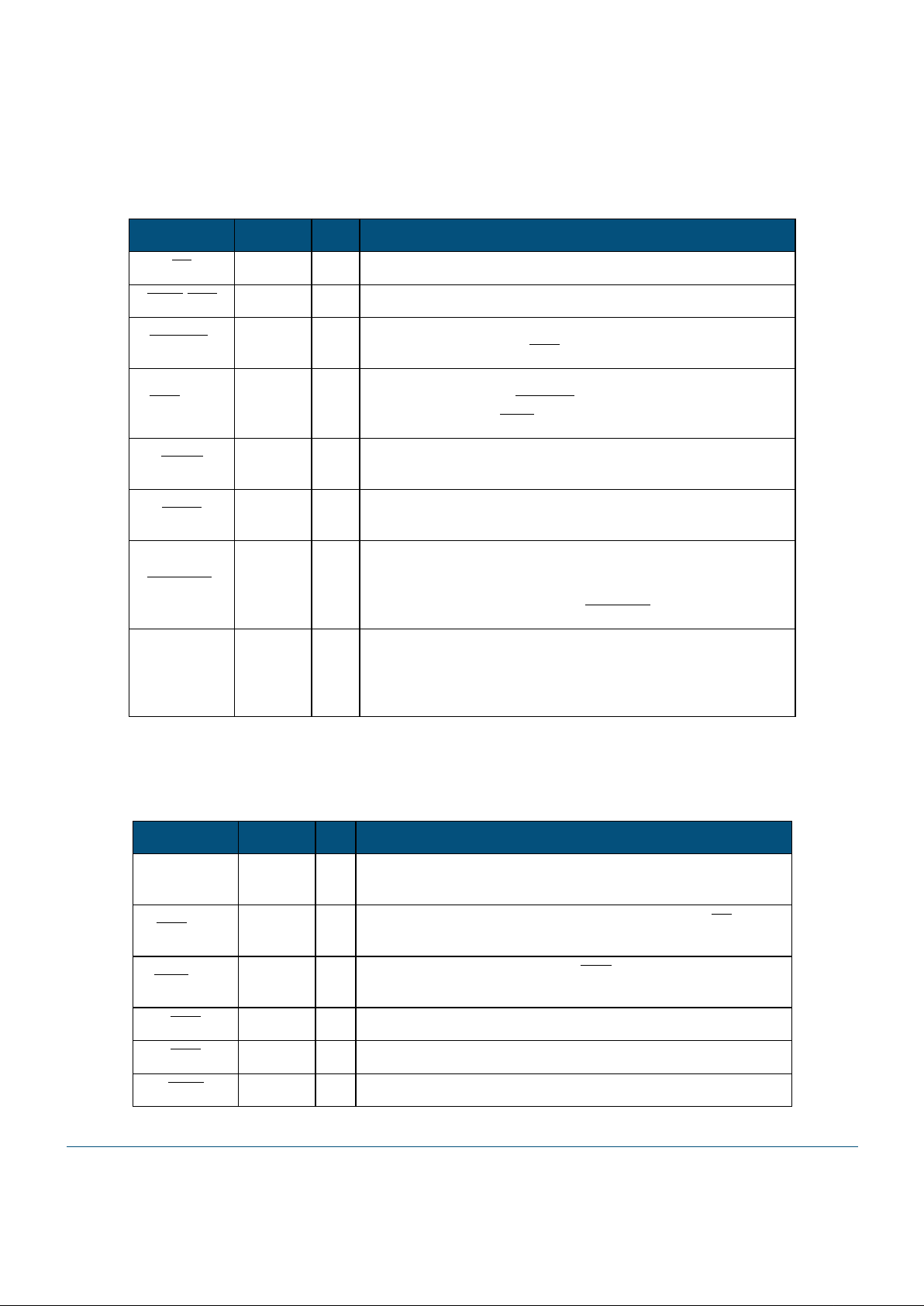
6.0 Timing Parameters
Figure 4: Clock and Synchronous Signals
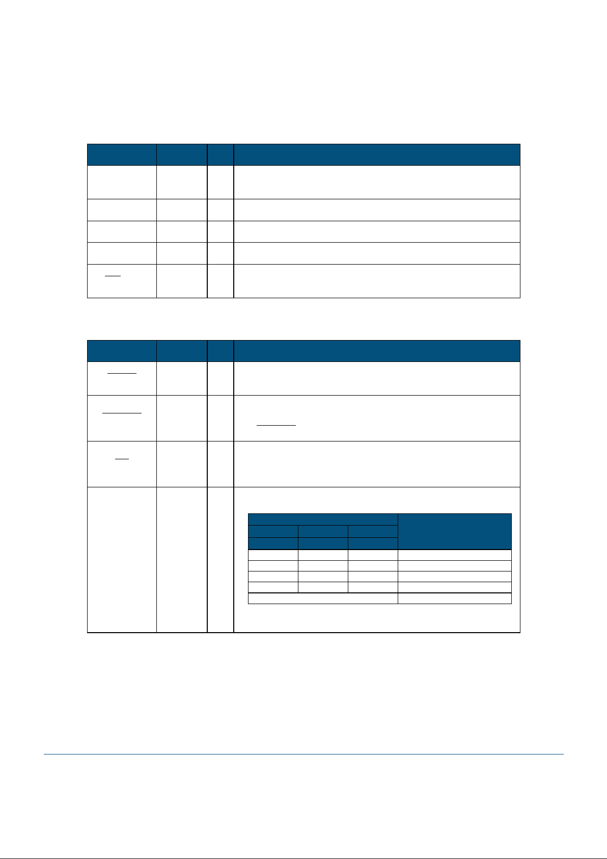
Figure 5: ALE Timing
:
Table 20: Capacitive Derating for Output and I/O Pins
Output Drive Limit Supply V oltage Derating
8mA 3.3 volt 0.019 ns/pF for loads > 50 pF
12mA 3.3 volt 0.017 ns/pF for loads > 50 pF
Table 21: Local Bus/M-Bus Timing Parameters for Vcc =3.3 Volts +/- 5%
75MHz
# Symbol Description Notes Min Max Units
1TCLCLK period 13.33 ns
2TCHLCLK high time 4.5 ns
LOCAL CLOCK
INPUT SETUP/HOLD
OUTPUT VALID
OUTPUT DRIVE
OUTPUT FLOAT
T
H
T
SU
T
CL
T
C
T
CH
T
COZ
VALID
VALID
Tczo
T
COV
VALID
ALE
MAD
T
ALE
T
ASU
T
AH
ADDRESS
DS-UC01-0102.fm Page 19 Wednesday, June 30, 1999 7:30 PM
Page 20

20 V320USC B1 Datasheet Rev 1.02 DS-UC01-0102 Copyright © 1999 V3 Semiconductor Inc.
V320USC Datasheet
Timing Parameters
Notes:
1. Non-pipelined signals include MRDY
when the SYNC_RDY bit in the LB_BUS_CFG register is ‘0’, and BGNT when the BREQ_SYNC
register is ‘1’.
3TCLLCLK low time 4.5 ns
4T
SU
Synchronous input setup 2.5 ns
4a T
SU
Synchronous input setup for nonpipelined signals
19ns
5THSynchronous input hold 1.5 ns
6T
COV
LCLK to output valid delay 9 ns
7T
CZO
LCLK to output driving delay 9 ns
8T
COZ
LCLK to high impedance delay 12 ns
9T
ALE
ALE pulse width TCH-1 TCH+2 ns
10 T
ASU
Address to ALE setup time T
CH
ns
11 T
AH
Address hold time from ALE TCL-4 ns
Table 22: PCI Bus Timing Parameters for Vcc = 3.3 Volts +/- 10%
# Symbol Description Notes Min Max Units
1TCPCLK period 20 ns
2TSUSynchronous input setup to PCLK 1 7 ns
2a T
SU
Synchronous input setup to PCLK (GNT)10ns
3THSynchronous input hold from PCLK 0 ns
4T
COV
PCLK to output valid delay 2 2 11 ns
4a T
COV
PCLK to output valid delay (REQ) 2 12 ns
5T
CZO
PCLK to output driving delay 2 11 ns
6T
COZ
PCLK to high impedance delay 3 14 ns
7T
RST
Reset period 16·T
C
Table 21: Local Bus/M-Bus Timing Parameters for Vcc =3.3 Volts +/- 5%
75MHz
# Symbol Description Notes Min Max Units
DS-UC01-0102.fm Page 20 Wednesday, June 30, 1999 7:30 PM
Page 21

V320USC Datasheet
Revision History
Copyright © 1999 V3 Semiconductor Inc. V320USC B1 Datasheet Rev 1.02 DS-UC01-0102 21
6.1 Serial EEPROM Port TImings
The clock for the serial EEPROM interface is derived by dividing the PCI bus clock. The waveforms generated are shown in
Figure 6.
Figure 6: Serial EEPROM Waveforms and Timings
7.0 Revision History
© V3 Semiconductor Inc., 1999
V320USC is a trademark of V3 Semiconductor Inc.
All other trademarks are the property of their respective owners.
V3 Semiconductor reserves the right to make changes to its products or specifications at any time, without notice, in order to improv e design
or performance and to supply the best possible product. V3 does not assume any responsibility for use of any circuitry described other than
the circuitry embodied in a V3 product. The Company makes no representations that circuitry described herein is free from patent
infringement or other rights of third parties which may result from its use. No license is granted by implication or otherwise under any patent,
patent rights, or other rights of V3 Semiconductor.
Table 23: Revision History
Revision
Number
Date Comments and Changes
0.8 Dec 98 First pre-silicon revision of preliminary data sheet.
0.9 Jan 99 First pre-silicon release with Super-H™ processor information.
1.00 Mar 99
Remove “Preliminary” watermark; Update Table 2: Pin Types;
Update Table 3: Signal Descriptions;
Update Table 9: Local Bus Signals DC Operating Specifications.
1.01 Apr 99 Update diagrams; update tables, register data; add M bus data.
1.02 June 99 Update diagrams, update tables, and update register data for B1 step.
SCL
SDA
START CONDITION
STOP CONDITION
512 PCI BUS
CLOCKS
256 PCI BUS
CLOCKS
256 PCI BUS
CLOCKS
DS-UC01-0102.fm Page 21 Wednesday, June 30, 1999 7:30 PM
 Loading...