

Page 1
April 1998
Revised October 1998
V320 8-Bit Registered Bus Transceiver
© 1998 Fairchild Semiconductor Corporation DS500149.prf www.fairchildsemi.com
V320
8-Bit Registered Bus Transcei ver
General Description
The V320 is an 8-bit universal bus transceiver designed for
high speed interfa cing with th e VME 320 ba ckplane. It has
output character isti cs op timi ze d for d rivi ng la rge c apa ci tive
loads and features modified input levels (V
IH/VIL
) for
increased noise immunity and reduced input skew. The
V320 functionalit y consists of bus transceiver circuits with
3-STATE, D-type flip-flops, an d control circuitry arranged
for multiplexed t ransmiss ion of d ata direct ly from the inp ut
bus or from the internal r egisters . Data on the A or B bus
will be clocked into the registers as the appropriate clock
pin goes to a high logic lev el. OE
and direction pins a re
provided to control the transceiver function. In the transceiver mode, dat a p re sen t a t the high impedan ce p or t m ay
be store d in ei the r th e A or B re gis t er or in bo t h . Th e s ele c t
controls can multiplex stored and real time (transparent
mode) data. The direction control dete rmines which bus
will receive data when the enable control OE
is active
LOW. In the isolation mode (OE
HIGH) A data may be
stored in the B regis ter and /or B data may be st ored in t he
A register.
Features
■ Independent registers for A and B buses
■ Multiplexed real-time and stored data
■ Guaranteed output skew
■ Guaranteed MOS (Multiple Output Switching) Specifica-
tions
■ Output switching specified for both 50 pF and 250 pF,
and 500 pF loads
■ Guaranteed simultaneous switching noise level (V
OLP
/
V
OLV
) and dynamic threshold performance (V
IHD/VILD
)
■ Glitch free power up/down high impedance for live insertion
■ BiCMOS technology for high drive and lo w power dissipation
■ −40°C to 85°C commercial temperature and V
CC
specifi-
cations
■ Modified specifications across V
CC
and temperature
(V
CC
= 5.0V ±1%, T = 25°C ± 20°C) present more realis-
tic system conditions
■ Available in TSSOP (MTC)
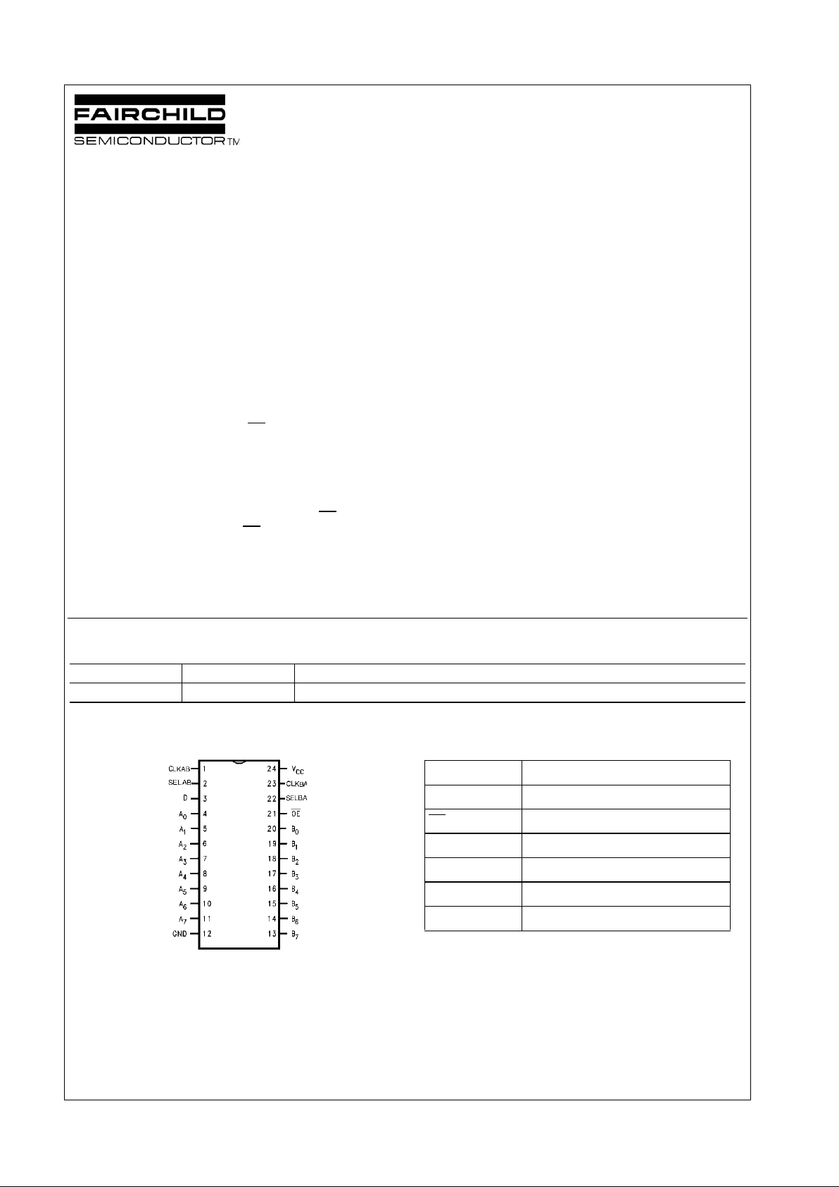
Ordering Code:
Device also available in Tape and Reel. Specify by appe nding suffix letter “X” to the ordering code.
Connection Diagram Pin Descriptions
Order Number Package Number Package Description
V320MTC MTC24 24-Lead Thin Shrink Small Outline Package, JEDEC MO-153, 4.4mm Wide
Pin Names Description
D Direction A-to-B (High) B-to A (Low)
OE
Output Enable (Active LOW)
CLKAB/SELAB A-to-B Clock/Select
CLKBA/SELBA B-to-A Clock/Select
A0–7 A Inputs/Outputs (TTL)
B0–7 B Inputs/Outputs (TTL)
Page 2
www.fairchildsemi.com 2
V320
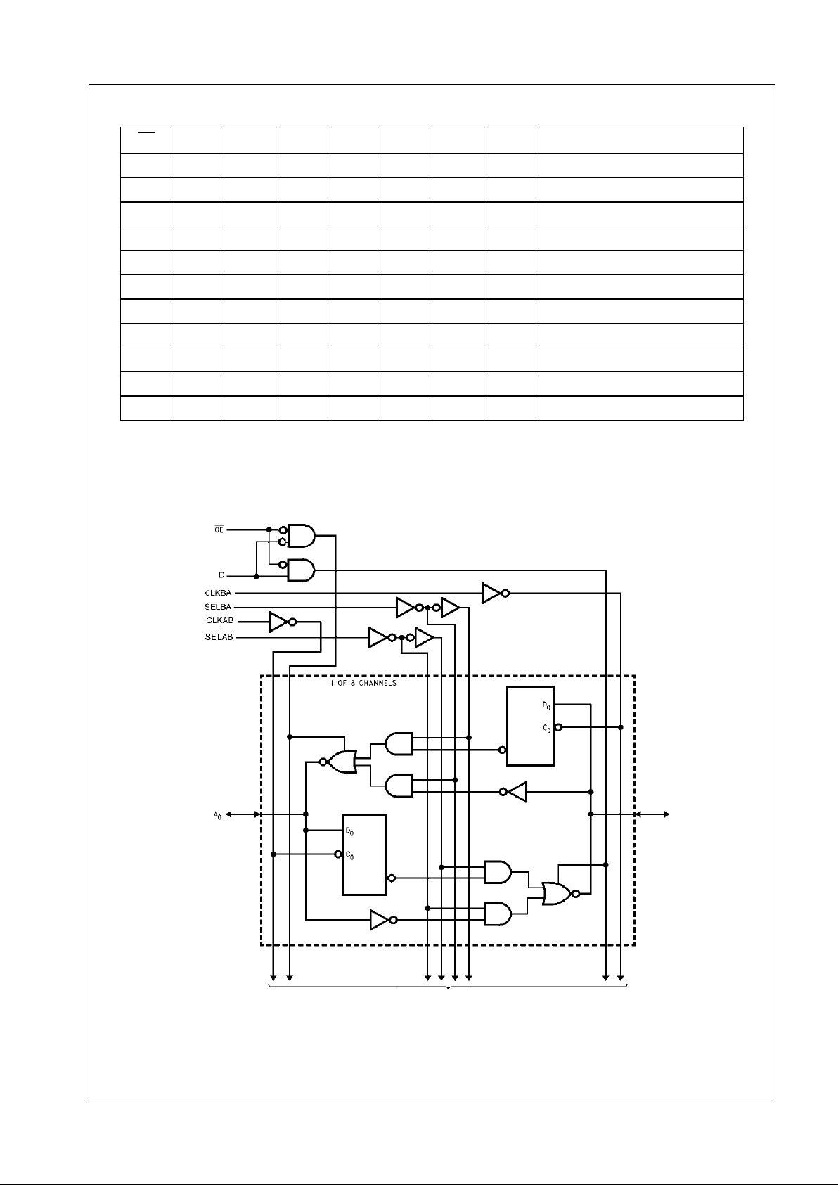
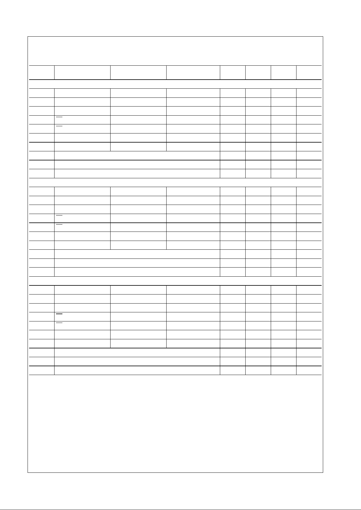
Functional Table
L = Low
H = High
LH = Low to High transition
X = Don’t Care
Logic Diagram
Please note that this diagram is pr ov ided only for the unders t anding of logic opera t ions and should not be us ed to estimate propa gation delays.
OE D SELAB SELBA CLKAB CLKBA
A
0–A7B0–B7
Function
H X X X H or L H or L Isolation
H X X X LH X Input Input CLK A Data into A
HXXXXLH CLK B Data into A Reg.
LHLXXX A to B – Transparent
L H L X LH X CLK A Data into A Reg.
L H H X H or L X Input Output A Reg. to B (Storage)
L H H X LH X CLK A Data into A Reg. and B output
L L X L X X B to A – Transparent
L L X L X LH CLK B Data into B Reg.
L L X H X H or L Output Input B Reg. to A (Storage)
L L X H X LH CLK B Data into B Reg.and A output
Page 3
3 www.fairchildsemi.com
V320
Absolute Maximum Ratings(Note 1) Recommended Operating
Conditions
Note 1: Absolute maxim um ratings are values be yond which the device
may be damaged or have its useful life impaired. Functional operation
under these conditions is not impli ed.
Note 2: Either voltage limit or current limit is sufficient to protect inputs.
DC Electrical Characteristics (4.5V < VCC ≤ 5.5V)
Over Recommended Operating Free-Air Temperature Range (Unless Otherwise Noted)
Note 3: Extended Characteristics (4.95 > VCC > 5.05, T = 25°C ± 20°C)
DC Input Voltage (VI) −0.5V to +7.0V
DC Output Voltage (V
O
)
Outputs 3-STATE −0.5V to +7.0V
Outputs Active (Note 2) −0.5V to V
CC
+0.5V
DC Output Sink Current into
A-port/B-port I
OL
64 mA
DC Output Source Current from
A-port/B-port I
OH
−32 mA
DC Input Diode Current (I
IK
)
V
I
< 0
V
−30 mA to +5.0 mA
ESD Rating typical > 2000V
Storage temperature (T
STG
) −65° C to +15°C
Max I
OL
(Current Applied to a
LOW Output) 2 X I
OL
Spec.
Supply Voltage V
CC
Operating V
CC
4.5V to 5.5V
Minimum Input Edge Rate
Data Input 50 mV/ns
Enable 20 mV/ns
Clock 100 mV/ns
Operating Temperature (T
A
) −40°C to +85°C
Symbol Parameter
V
CC
(V)
Min Typ Max Units Conditions
VIHB-Port/A-Port HIGH Level Input Voltage 4.5–5.5 2.0 V Recognized HIGH Signal
4.95–5.05 1.8
(Note 3)
VILB-Port/A-Port LOW Level Input Vo ltage 4.5–5.5 0.8 V Recognized LOW Signal
4.95–5.05 1.2
(Note 3)
VOHB-Port/A-Port HIGH Level Output Voltage 4.5 2.5 V −3 mA
4.5 2.0 −32 mA
I
OH
B-Port/A-Port High Level Output Current Drive 4.5 −32 mA VOH = 2.0V
VOLB-Port/A-Port LOW Level Output Voltage 4.5 0.55 V 64 mA
I
OL
B-Port/A-Port Low Level Output Current Drive
(Sink)
4.5 64 mA VOL = 0.55V
I
OS
B-Port/A-Port Short Circuit Current 5.5 −100 −275 mA V
OUT
= 0.0V
I
OFF
A-Port and
Control Pins
Power-OFF Leakage Current 0.0 100uA uA V
OUT
= 5.5V, All Others
GND
I
CCH
B-Port/A-Port Quiescent Power Supply Current 5.5 250 uA All Outputs HIGH
I
CCI
B-Port/A-Port B-Port/A-Port 5.5 30 mA All Outputs LOW
I
CCZ
B-Port/A-Port 3-STATE Power Supply Current 5.5 50 uA All Outputs 3-STATE
Page 4
www.fairchildsemi.com 4
V320
Capacitance and Dynamic Switching Characteristics
Over Recommended Operating Free-Air Temperature Range (Unless Otherwise Noted)
AC Operating Requirements
Over recommended ranges of supply voltage and operating free-air temperature
Note 4: CL = 50 pF
Symbol Parameter Min Typ Max U nit s Conditions
TA = 25°C
C
IN
Input Capacitance (Control Pin) 5 pF VCC = 5.0V VI = VCC or 0
C
I/O
Output Capacitance (A and B ports) 11 pF VCC = 5.0V VI = VCC or 0
Output Switching Noise (Ground Bounce)
V
OLP
Quiet Output Dynamic Peak V
OL
0.8 V VCC = 5.0V, T= 25°C
V
OLV
Quiet Output Dynamic Valley V
OL
−1.2 V CL = 50 pF
V
OHV
Quiet Output Dynamic Valley V
OH
2.5 V
Input Noise Immu nity (Dynamic Threshold)
V
IHD
High Level Threshold Movement 2.2 V VCC = 5.0V, T= 25°C
V
ILD
Low Level Threshold Movement 0.5 V CL = 50 pF
Symbol Min Typ Max Units
f
CLOCK
Max Clock Frequency 200 (Note 4) MHz
t
WIDTH
Pulse Duration HIGH or LOW 3.0 ns
t
SU
Setup Time Bus to CLKAB/CLKBA 1.5 ns
t
HOLD
Hold Time Bus to CLKAB/CLKBA 1.0 ns
Page 5

5 www.fairchildsemi.com
V320
AC Electrical Characteristics
(−40°C to 85°C, V
CC
= 4.5V to 5.5V) 1 Output Switching
Note 5: 3-STATE delays are domina ted by the RC Network (50 0 Ω/ 250 pF, or 500 Ω/ 500 pF) on the o utput and thus have bee n excluded from this
datasheet.
Symbol
From
(Input)
Mode
To
(Output)
Min Typ Max Units
Output Load: CL = 50 pF, RL= 500Ω, 1 Output Switching
t
PLH
, t
PHL
CLKAB/CLKBA Register Bus A or B 1.7 5.6 ns
t
PLH
, t
PHL
Bus A or B Transparent Bus A or B 1.5 4.8 ns
t
PLH
, t
PHL
SELAB/SELBA Select Bus Bus A or B 1.5 5.9 ns
t
PLZ
, t
PHZ
OE Output Disable Bus A or B 1.5 6.0 ns
t
PZH
, t
PZL
OE Output Enable Bus A or B 1.5 6.3 ns
t
PLZ
, t
PHZ
Direction (D) Dir. Disable Bus A or B 1.5 6.0 ns
t
PZH
, t
PZL
Direction (D) Dir. Enable Bus A or B 1.5 6.3 ns
t
RISE
Transition Time, Outputs (1V to 2V) 0.3 1.2 ns
t
FALL
Transition Time, Outputs (1V to 2V) 0.3 1.4 ns
Output Load: CL = 250 pF, RL = 500Ω, 1 Output Switching
t
PLH
, t
PHL
CLKAB/CLKBA Register Bus A or B 2.0 7.5 ns
t
PLH
, t
PHL
Bus A or B Transparent Bus A or B 2.0 7.0 ns
t
PLH
, t
PHL
SELAB/SELBA Select Bus Bus A or B 2.0 7.5 ns
t
PLZ
, t
PHZ
OE Output Disable Bus A or B (Note 5) (Note 5) ns
t
PZH
, t
PZL
OE Output Enable Bus A or B 2.0 8.0 ns
t
PLZ
, t
PHZ
Direction (D) Dir. Disable Bus A or B (Note 5) (Note 5) ns
t
PZH
, t
PZL
Direction (D) Dir. Enable Bus A or B 2.0 8.3 ns
t
RISE
Transition Time, Outputs (1V to 2V) 1.7 3.9 ns
t
FALL
Transition Time, Outputs (1V to 2V) 0.8 3.1 ns
Output Load: CL = 500 pF, RL = 500Ω, Output Switching
t
PLHtPHL
CLKAB/CLKBA Register Bus A or B 3.0 12.2 ns
t
PLHtPHL
Bus A or B Transparent Bus A or B 3.0 11.6 ns
t
PLHtPHL
SELAB/SELBA Select Bus Bus A or B 3.0 12.4 ns
t
PLZ
, t
PHZ
OE Output Disable Bus A or B (Note 5) (Note 5) ns
t
PZH
, t
PZL
OE Output Enable Bus A or B 3.0 12.6 ns
t
PLZ
, t
PHZ
Direction (D) Dir. Disable Bus A or B (Note 5) (Note 5) ns
t
PZH
, t
PZL
Direction (D) Dir. Enable Bus A or B 6.3 13.2 ns
t
RISE
Transition Time, Outputs (1V to 2V) 3.5 7.2 ns
t
FALL
Transition Time, Outputs (1V to 2V) 1.4 5.1 ns
Page 6

www.fairchildsemi.com 6
V320
AC Electrical Characteristics
(−40°C to 85°C, V
CC
= 4.5V to 5.5V) 8 Output Switching
Note 6: Skew i s defined as th e absolute value of the differe nc e between the actual propagation delays f or any two out puts of the same device. The sp ec if i-
cation applies t o outputs switchin g in t he same direction also.
Note 7: Device to Device Ske w is define d as the absolute v alue of the diffe rence be tween the actua l propagat ion delay s for any tw o outputs from any two
devices.
Note 8: 3-STATE delays are dominated by the RC Network (500 Ω/ 25 0 pF, o r 500 Ω/ 500 pF) on th e output and thus hav e been excluded from th is
datash eet.
Symbol
From
(Input)
Mode
To
(Output)
Min Typ Max Units
Output Load: CL = 50 pF, RL = 500Ω, 8 Outputs Switching
t
PLH
, t
PHL
CLKAB/CLKBA Register Bus A or B 1.5 6.6 ns
t
PLH
, t
PHL
Bus A or B Transparent Bus A or B 1.5 6.3 ns
t
PLH
, t
PHL
SELAB/SELBA Select Bus Bus A or B 1.5 6.6 ns
t
PLZ
, t
PHZ
OE Output Disable Bus A or B 1.5 6.6 ns
t
PZH
, t
PZL
OE Output Enable Bus A or B 1.5 6.6 ns
t
PLZ
, t
PHZ
Direction (D) Dir. Disable Bus A or B 1.5 6.6 ns
t
PZH
, t
PZL
Direction (D) Dir. Enable Bus A or B 1.5 7.6 ns
t
OSHL
Output to Output Skew (Note 6) 1.3 ns
t
OSHL
Output to Output Skew (Note 6) 1.1 ns
t
RISE
Transition Time, Outputs (1V to 2V) 0.5 1.5 ns
t
FALL
Transition Time, Outputs (1V to 2V) 0.4 1.9 ns
Output Load: CL = 250 pF, RL = 500Ω, 8 Outputs Switching
t
PLH
, t
PHL
CLKAB/CLKBA Register Bus A or B 2.5 11.2 ns
t
PLH
, t
PHL
Bus A or B Transparent Bus A or B 2.5 9.5 ns
t
PLH
, t
PHL
SELAB/SELBA Select Bus Bus A or B 2.5 11.2 ns
t
PLZ
, t
PHZ
OE Output Disable Bus A or B (Note 8) (Note 8) ns
t
PZH
, t
PZL
OE Output Enable Bus A or B 2.5 11.5 ns
t
PLZ
, t
PHZ
Direction (D) Dir. Disable Bus A or B (Note 8) (Note 8) ns
t
PZH
, t
PZL
Direction (D) Dir. Enable Bus A or B 2.5 13.5 ns
t
OSHL
Output to Output Skew (Note 8) 2.5 ns
t
OSLH
Output to Output Skew (Note 8) 2.0 ns
t
RISE
Transition Time, Outputs (1V to 2V) 2.0 5.5 ns
t
FALL
Transition Time, Outputs (1V to 2V) 1.4 4.4 ns
Output Load: CL = 500 pF, RL = 500Ω, 8 Outputs Switching
t
PLH
, t
PHL
CLKAB/CLKBA Register Bus A or B 3.5 17 .0 ns
t
PLH
, t
PHL
Bus A or B Transparent Bus A or B 3.5 15.9 ns
t
PLH
, t
PHL
SELAB/SELBA Select Bus Bus A or B 3.5 17.0 ns
t
PLZ
, t
PHZ
OE Output Disable Bus A or B (Note 8) (Note 8) ns
t
PZH
, t
PZL
OE Output Enable Bus A or B 3.5 18.5 ns
t
PLZ
, t
PHZ
Direction (D) Dir. Disable Bus A or B (Note 8) (Note 8) ns
t
PZH
, t
PZL
Direction (D) Dir. Enable Bus A or B 3.5 22.3 ns
t
OSHL
Output to Output Skew (Note 6) 3.9 ns
t
OSLH
Output to Output Skew (Note 6) 3.1 ns
t
RISE
Transition Time, Outputs (1V to 2V) 4.4 7.8 ns
t
FALL
Transition Time, Outputs (1V to 2V) 2.5 6.6 ns
Page 7
7 www.fairchildsemi.com
V320
Extended AC Electrical Characteristics
(5°C to 45°C, V
CC
= 4.95V to 5.05V), 1 Output Switching
Note 9: 3-STATE delays are domina ted by the RC Network (50 0 Ω/ 250 pF, or 500 Ω/ 500 pF) on the o utput and thus have bee n excluded from this
datasheet.
Note 10: Device t o Device Skew is defined as the absolute value of the difference between the actual propag at ion delays for any two out puts from a ny two
devices.
Symbol
From
(Input)
Mode
To
(Output)
Min Typ Max Units
Output Load: CL = 50 pF, RL = 500Ω, 1 Output Switching
t
PLH
, t
PHL
CLKAB/CLKBA Register Bus A or B 1.5 5.2 ns
t
PLH
, t
PHL
Bus A or B Transparent Bus A or B 1.5 4.3 ns
t
PLH
, t
PHL
SELAB/SELBA Select Bus Bus A or B 2.0 4.8 ns
t
PLZ
, t
PHZ
OE Output Disable Bus A or B 1.5 6.0 ns
t
PZH
, t
PZL
OE Output Enable Bus A or B 2.2 5.0 ns
t
PLZ
, t
PHZ
Direction (D) Dir. Disable Bus A or B 1.5 6.0 ns
t
PZH
, t
PZL
Direction (D) Dir. Enable Bus A or B 2.2 5.2 ns
t
PV
Device to Device Skew (Note 10) 2.0 ns
t
RISE
Transition Time, Outputs (1V to 2V) 3.0 1.2 ns
t
FALL
Transition Time, Outputs (1V to 2V) 0.4 1.2 ns
Output Load: CL = 250 pF, RL = 500Ω, 1 Output Switching
t
PLH
, t
PHL
CLKAB/CLKBA Register Bus A or B 2.5 7.4 ns
t
PLH
, t
PHL
Bus A or B Transparent Bus A or B 2.5 6.7 ns
t
PLH
, t
PHL
SELAB/SELBA Select Bus Bus A or B 3.0 7.2 ns
t
PLZ
, t
PHZ
OE Output Disable Bus A or B (Note 9) (Note 9) ns
t
PZH
, t
PZL
OE Output Enable Bus A or B 3.2 7.2 ns
t
PLZ
, t
PHZ
Direction (D) Dir. Disable Bus A or B (Note 9) (Note 9) ns
t
PZH
, t
PZL
Direction (D) Dir. Enable Bus A or B 3.2 8.1 ns
t
PV
Device to Device Skew (Note 10) 2.5 ns
t
RISE
Transition Time, Outputs (1V to 2V) 2.1 3.5 ns
t
FALL
Transition Time, Outputs (1V to 2V) 1.0 2.5 ns
Output Load: CL = 500 pF, RL = 500Ω, 1 Output Switching
t
PLH
, t
PHL
CLKAB/CLKBA Register Bus A or B 3.5 10.6 ns
t
PLH
, t
PHL
Bus A or B Transparent Bus A or B 3.5 10.0 ns
t
PLH
, t
PHL
SELAB/SELBA Select Bus Bus A or B 4.0 10.6 ns
t
PLZ
, t
PHZ
OE Output Disable Bus A or B (Note 9) (Note 9) ns
t
PZH
, t
PZL
OE Output Enable Bus A or B 4.2 10.5 ns
t
PLZ
, t
PHZ
Direction (D) Dir. Disable Bus A or B (Note 9) (Note 9) ns
t
PZH
, t
PZL
Direction (D) Dir. Enable Bus A or B 4.2 11.3 ns
t
PV
Device to Device Skew 5.0 ns
t
RISE
Transition Time, Outputs (1V to 2V) 3.8 6.4 ns
t
FALL
Transition Time, Outputs (1V to 2V) 1.7 3.8 ns
Page 8

www.fairchildsemi.com 8
V320
Extended AC Electrical Characteristics
(5°C to 45°C, V
CC
= 4.95V to 5.05V), 8 Outputs Switching
Note 11: 3-STATE delays are dominated by the RC Netw ork (500 Ω/ 250 p F, or 500 Ω/ 500 pF) on the output and thus have been e xcluded from th is
datash eet.
Note 12: Skew is def ined as the absolute v alue of the difference between the actual propagation delays for any two outputs of the sam e device. The specifi-
cation applies t o outputs switchin g in t he same direction also.
Note 13: Device to Device Skew is defi ned as the ab s olute value of t he difference b et w een the actual propagation delays for any two outputs from any two
devices.
Symbol
From
(Input)
Mode
To
(Output)
Min Typ Max Units
Output Load: CL = 50 pF, RL = 500Ω, 8 Outputs Switching
t
PLH
, t
PHL
CLKAB/CLKBA Register Bus A or B 2.5 6.2 ns
t
PLH
, t
PHL
Bus A or B Transparent Bus A or B 2.5 5.4 ns
t
PLH
, t
PHL
SELAB/SELBA Select Bus Bus A or B 2.5 5.7 ns
t
PLZ
, t
PHZ
OE Output Disable Bus A or B 1.5 6.0 ns
t
PZH
, t
PZL
OE Output Enable Bus A or B 2.5 5.7 ns
t
PLZ
, t
PHZ
Direction (D) Dir. Disable Bus A or B 1.5 6.0 ns
t
PZH
, t
PZL
Direction (D) Dir. Enable Bus A or B 2.5 7.2 ns
t
OSHL
Output to Output Skew (Note 12) 1.1 ns
t
OSLH
Output to Output Skew (Note 12) 0.9 ns
t
PV
Device to Device Skew (Note 13) 2.5 ns
t
RISE
Transition Time, Outputs (1V to 2V) 0.5 1.3 ns
t
FALL
Transition Time, Outputs (1V to 2V) 0.6 1.4 ns
Output Load: CL = 250 pF, RL = 500Ω, 8 Outputs Switching
t
PLH
, t
PHL
CLKAB/CLKBA Register Bus A or B 3.5 10 .5 ns
t
PLH
, t
PHL
Bus A or B Transparent Bus A or B 3.5 10.5 ns
t
PLH
, t
PHL
SELAB/SELBA Select Bus Bus A or B 3.5 10.5 ns
t
PLZ
, t
PHZ
OE Output Disable Bus A or B (Note 11) (Note 11) ns
t
PZH
, t
PZL
OE Output Enable Bus A or B 3.5 10.5 ns
t
PLZ
, t
PHZ
Direction (D) Dir. Disable Bus A or B (Note 11) (No te 11) ns
t
PZH
, t
PZL
Direction (D) Dir. Enable Bus A or B 3.5 14.8 ns
t
OSHL
Output to Output Skew (Note 12) 2.3 ns
t
OSLH
Output to Output Skew (Note 12) 1.9 ns
t
PV
Device to Device Skew(Note 13) 4.0 ns
t
RISE
Transition Time, Outputs (1V to 2V) 2.7 4.7 ns
t
FALL
Transition Time, Outputs (1V to 2V) 1.8 3.7 ns
Output Load: CL = 500 pF, RL = 500Ω, 8 Outputs Switching
t
PLH
, t
PHL
CLKAB/CLKBA Register Bus A or B 5.0 15 .3 ns
t
PLH
, t
PHL
Bus A or B Transparent Bus A or B 5.0 13.6 ns
t
PLH
, t
PHL
SELAB/SELBA Select Bus Bus A or B 5.0 15.3 ns
t
PLZ
, t
PHZ
OE Output Disable Bus A or B (Note 11) (Note 11) ns
t
PZH
, t
PZL
OE Output Enable Bus A or B 5.0 15.1 ns
t
PLZ
, t
PHZ
Direction (D) Dir. Disable Bus A or B (Note 11) (No te 11) ns
t
PZH
, t
PZL
Direction (D) Dir. Enable Bus A or B 5.0 19.4 ns
t
OSHL
Output to Output Skew (Note 12) 3.5 ns
t
OSLH
Output to Output Skew (Note 12) 2.9 ns
t
PV
Device to Device Skew 5.0 ns
t
RISE
Transition Time, Outputs (1V to 2V) 4.6 7.0 ns
t
FALL
Transition Time, Outputs (1V to 2V) 2.9 4.9 ns
Page 9

9 www.fairchildsemi.com
V320
AC Loading and Waveforms
*Includes jig and p robe capacitance
FIGURE 1. Standard AC Test Load
FIGURE 2. Test Input Signal Levels
Input Pulse Requirements
Test Input Signal Requirements
FIGURE 3. Propagation Delay Waveforms for Inverting
and Non-Inverting Functions
FIGURE 4. Propagation Delay,
Pulse Width Waveforms
FIGURE 5. 3-STATE Output HIGH
and LOW Enable and Disable Times
FIGURE 6. Setup Time, Hold Time
and Recovery Time Waveforms
Amplitude Rep. Rate t
W
t
r
t
f
3.0V 1 MHz 500 ns 2.5 ns 2.5 ns
Page 10

Fairchild does not assume any responsibility for use of any circuitry described, no circuit patent licenses are implied and Fairchild reserves the right at any time without notice to change said circuitry and specifications.
V320 8-Bit Registered Bus Transceiver
LIFE SUPPORT POLICY
FAIRCHILD’S PRODUCTS ARE NOT AUTHORIZED FOR USE AS CRITICAL COMPONENTS IN LIFE SUPPORT
DEVICES OR SYSTEMS WITHOUT THE EXPRESS WRITTEN APPROVAL OF THE PRESIDENT OF FAIRCHILD
SEMICONDUCTOR CORPORATION. As used herein:
1. Life support de vices o r syste ms a re device s or syste ms
which, (a) are intended for surgical implant into the
body, or (b) support or sustain life, and (c) whose failure
to perform when properly used in accordance with
instructions for use provided in the labeling, can be reasonably expected to result in a significant injury to the
user.
2. A critical compon ent in any com ponen t of a life su pport
device or system whose failure to perform can be reasonably expect ed to ca use the fa ilure of the li fe su pp ort
device or system, or to affect its safety or effectiveness.
www.fairchildsemi.com
Physical Dimensions inches (millimeters) unless otherwise noted
24-Lead Thin Shrink Small Outline Package, JEDEC MO-153, 4.4mm Wide
Package Number MTC24
 Loading...