

Datasheet V9MLN41206WT, V9MLN41206WH, V9MLN41206WA, V5.5MLN41206WT, V5.5MLN41206WH Datasheet (LITTELFUSE)
...Page 1
3
SURFACE MOUNT
VARISTORS
Surface Mount Varistors
151
www.littelfuse.com
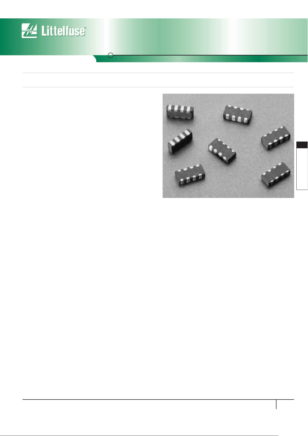
Multiline Transient Voltage Surge Suppressor
MLN SurgeArray™Suppressor
The MLN SurgeArray™Suppressor is designed to help protect components from transient voltages that exist at the circuit board level. This
device provides four independent suppressors in a single “1206” leadless
chip in order to reduce part count and placement time as well as save
space on printed circuit boards.
SurgeArray™devices are intended to suppress ESD, EFT and other
transients in order to protect integrated circuits or other sensitive
components operating at any voltage up to 18VDC. SurgeArray devices
are rated to the IEC 61000-4-2 human body model ESD to help products
attain EMC compliance. The array offers excellent isolation and low
crosstalk between sections.
The inherent capacitance of the SurgeArray Suppressor permits it to
function as a filter/suppressor, thereby replacing separate zener/
capacitor combinations.
The MLN array is manufactured using the Littelfuse Multilayer technology
process and is similar to the Littelfuse ML and MLE Series of discrete
leadless chips.
The MLN can also be provided in a Dual version. Contact Littelfuse
for information.
Features
• Four Individual Devices in One 1206 Chip
• ESD Rated to IEC 61000-4-2 (Level 4)
• AC Characterized for Impedance and Capacitance
• Low Adjacent Channel Crosstalk, -55dB at 10MHz (Typ)
• Low Leakage (6nA at 5.5V, 30nA at 15V)
• Operating Voltage up to 18V
M(DC)
• -55
o
C to 125oC Operating Temperature Range
• Low-Profile, PCMCIA Compatible
Applications
• Data, Diagnostic I/O Ports
• Analog Signal/Sensor Lines
• Portable/Hand-Held Products
• Mobile Communications/Cellular Phones
• Computer/DSP Products
• Industrial Instruments Including Medical
Page 2
Multiline Transient Voltage Surge Suppressor
MLN SurgeArray™Suppressor
Surface Mount Varistors
152
www.littelfuse.com
Absolute Maximum Ratings
For ratings of individual members of a series, see device ratings and specifications table.
Continuous:
Steady State Applied Voltage: DC Voltage Range (V
M(DC)
). . . . . . . . . . . . . . . . . . . . . . . . . . . . . . . . . . . . . . . . . . . . . . . . . . . 18 V
Operating Ambient Temperature Range (TA) . . . . . . . . . . . . . . . . . . . . . . . . . . . . . . . . . . . . . . . . . . . . . . . . . . . . . . . . . . . . . -55 to 125
O
C
Storage Temperature Range (T
STG
) . . . . . . . . . . . . . . . . . . . . . . . . . . . . . . . . . . . . . . . . . . . . . . . . . . . . . . . . . . . . . . . . . . . -55 to 150
O
C
Device Ratings and Specifications Any Single Section
Temperature Derating
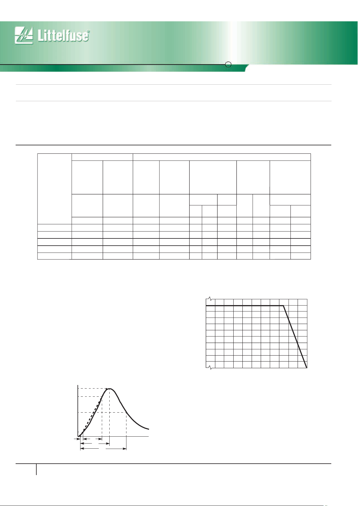
For applications exceeding 125oC ambient temperature, the peak surge
current and energy ratings must be reduced as shown in Figure 1.
MLN ARRAY UNITS
PA RT
NUMBER
MAX RATINGS (125
o
C) PERFORMANCE SPECIFICATIONS (25oC)
MAXIMUM
CONTINUOUS
WORKING
VO LTAGE
MAXIMUM
NON-
REPETITIVE
SURGE
CURRENT
(8/20µs)
MAXIMUM
CLAMPING
VO LTAGE
(AT NOTED
CURRENT
8/20µs)
MAXIMUM
NON-
REPETITIVE
SURGE
ENERGY
(10/1000µs)
TYPICAL
ESD SUPPRESSION
VOLTAGE (NOTE 1)
NOMINAL
VO LTAGE AT
1mA DC
CURRENT
CAPACITANCE
AT
1MHz (1V p-p)
V
M(DC)
I
TM
V
C
W
TM
(V) (A) (V) (J) (V) (V) (pF)
V5.5MLN41206
V9MLN41206
V14MLN41206
V18MLN41206
V18MLN41206L
430 520
250 300
140 175
100 125
NOTES:
1. Tested to IEC61000-4-2 Human Body Model (HBM) discharge test circuit. See explanation of Terms on page 7.
2. Direct discharge to device terminals (IEC preffered test method). See figure 2.
3. Corona discharge through air (represents actual ESD event)
4. Capacitance may be customized, contact Sales.
(See Fig. 3)
Peak
(NOTE 2)
8kV CONTACT
(NOTE 3)
15kV AIR
Clamp
(V)
Peak
(V)
(V)
VN(DC)
MIN
V
N(DC)
MAX
(NOTE 4)
C
TYP MAX
(pF)
45 75
5.5
9
14
18
18
30
30
30
30
20
7.1
11.0
15.9
22.0
25.0
9.3
16.0
20.3
28.0
35.0
60
95
110
165
200
35
50
55
60
95
45
75
85
100
130
0.1
0.1
0.1
0.1
0.05
15.5 at 2A
23 at 2A
30 at 2A
40 at 2A
50 at 1A
100
90
80
70
60
50
40
30
20
10
0
-55 50 60 70 80 90 100 110 120 130 140 150
PERCENT OF RATED VALUE
AMBIENT TEMPERATURE (oC)
FIGURE 1. PEAK CURRENT AND ENERGY DERATING CURVE
t
t
1
t
2
100
90
50
10
O
1 TIME
PERCENT OF PEAK VALUE
O1 = VIRTUAL ORIGIN OF WAVE
t
1
= VIRTUAL FRONT TIME = 1.25 x t
(IMPULSE DURATION)
t = TIME FROM 10% TO 90% OF PEAK
t
2
= VIRTUAL TIME TO HALF VALUE
EXAMPLE:
FOR AN 8/20µs CURRENT
WAVEFORM:
8µs = t
1
= VIRTUAL FRONT
20µs = t
2
= VIRTUAL TIME TO
HALF VALUE
TIME
FIGURE 2. PEAK PULSE CURRENT TEST WAVEFORM FOR CLAMPING VOLTAGE
Page 3
Typical Performance Curves Any Single Section
40
30
20
10
0
1 10 100 1000
NUMBER OF DISCHARGES
V
NOM
10,000
FIGURE 4. PRODUCT DISTRIBUTION OF CAPACITANCE (1MHz)
70
60
50
40
30
20
10
0
SAMPLES
CAPACITANCE (pF)
7060504030 35 45 55 65
Typical Performance Curves Any Single Section
FIGURE 5. V-I CHARACTERISTICS
FIGURE 6. PULSE RATING FOR LONG DURATION SURGES (ANY SINGLE SECTION)
90
80
70
60
50
40
30
20
10
0
VARISTOR VOLTAGE (V)
1.0E
-07
CURRENT (A)
1.0E
-06
1.0E
-05
1.0E
-04
1.0E
-03
1.0E
-02
1.0E
-01
1.0E
+00
1.0E
+01
1.0E
+02
MAXIMUM STANDBY CURRENT (LEAKAGE)
MAXIMUM CLAMP VOLTAGE
TYPICAL
1
2
10
100
10
3
10
4
10
5
10
6
∞
100
10
1
0.1
10 100 1000 10000
SQUARE WAVE PULSE DURATION ( µs)
SURGE CURRENT (A)
NUMBER OF SURGES
MLN SurgeArray™Suppressor
Surface Mount Varistors
Multiline Transient Voltage Surge Suppressor
153
www.littelfuse.com
3
SURFACE MOUNT
VARISTORS
Page 4

Multiline Transient Voltage Surge Suppressor
MLN SurgeArray™Suppressor
Surface Mount Varistors
154
www.littelfuse.com
Typical Performance Curves Any Single Section (Continued)
FIGURE 7. STANDBY CURRENT AT NORMALIZED VARISTOR VOLTAGE AND TEMPERATURE (ANY SINGLE SECTION)
FIGURE 8. CAPACITANCE vs FREQUENCY
FIGURE 9. EQUIVALENT SERIES RESISTANCE
100
10
0.1µA1µA10µA 100µA1mA
CURRENT (A)
NORMALIZED VARISTOR VOLTAGE (%)
-40oC
25
o
C
85
o
C
125
o
C
70
65
60
55
50
45
40
1GHz
100MHz
10MHz
1MHz
FREQUENCY
CAPACITANCE (pF)
1000
1MHz
FREQUENCY
OHMS
100
10
1
0.1
10MHz 100MHz 1GHz 10GHz
Page 5

Soldering Recommendations
The principal techniques used for the soldering of components in surface
mount technology are Infrared (IR) Reflow, Vapour Phase Reflow, and
Wave Soldering. Typical profiles are shown in Figures 12, 13 and 14.
When wave soldering, the MLN suppressor is attached to the circuit
board by means of an adhesive. The assembly is then placed on a conveyor and run through the soldering process to contact the wave. With IR
and Vapour Phase Reflow, the device is placed in a solder paste on the
substrate. As the solder paste is heated, it reflows and solders the unit to
the board.
The recommended solder for the MLN suppressor is a 62/36/2
(Sn/Pb/Ag), 60/40 (Sn/Pb), or 63/37 (Sn/Pb). Littelfuse also
recommends an RMA solder flux.
Wave soldering is the most strenuous of the processes. To avoid the
possibility of generating stresses due to thermal shock, a preheat stage
in the soldering process is recommended, and the peak temperature of
the solder process should be rigidly controlled.
Typical Performance Curves Any Single Section (Continued)
FIGURE 10. IMPEDANCE vs FREQUENCY
FIGURE 11. ADJACENT CHANNEL CROSSTALK
10000
1000
100
10
1
0.1
1MHz
10MHz
100MHz
1GHz
10GHz
FREQUENCY
IMPEDANCE (Z)
0
-20
-40
-60
-80
-100
-120
1kHz 100kHz10kHz 1MHz 10MHz 100MHz 1GHz
FREQUENCY
CROSSTALK (dB)
VIN = 1V
RMS
Z = 50Ω
When using a reflow process, care should be taken to ensure that the
MLN chip is not subjected to a thermal gradient steeper than 4 degrees
per second; the ideal gradient being 2 degrees per second. During the
soldering process, preheating to within 100 degrees of the solders peak
temperature is essential to minimize thermal shock. Examples of the soldering conditions for the MLN array of suppressors are given in the
tables below.
Once the soldering process has been completed, it is still necessary to
ensure that any further thermal shocks are avoided. One possible cause of
thermal shock is hot printed circuit boards being removed from the solder
process and subjected to cleaning solvents at room temperature. The
boards must be allowed to gradually cool to less than 50oC before cleaning.
MLN SurgeArray™Suppressor
Surface Mount Varistors
Multiline Transient Voltage Surge Suppressor
155
www.littelfuse.com
3
SURFACE MOUNT
VARISTORS
Page 6

Multiline Transient Voltage Surge Suppressor
MLN SurgeArray™Suppressor
Surface Mount Varistors
156
www.littelfuse.com
FIGURE 12. IR REFLOW SOLDER PROFILE
TEMPERATURE (
o
C)
TIME (MINUTES)
250
200
150
100
50
0
0 0.5 1.0 1.5 2.0 2.5 3.0 3.5 4.0
MAXIMUM
PREHEAT DWELL
PREHEAT ZONE
TEMPERATURE 222
o
C
RAMP RATE
<2
o
C/s
40-80
SECONDS
ABOVE 183
o
C
FIGURE 14. VAPOR PHASE SOLDER PROFILE
TEMPERATURE (
o
C)
TIME (MINUTES)
250
200
150
100
50
0
0 0.5 1.0 1.5 2.0 2.5 3.0 3.5
RAMP RATE
PREHEAT ZONE
>50
o
C/s
MAXIMUM
TEMPERATURE 222
o
C
40-80
SECONDS
ABOVE 183
o
C
FIGURE 13. WAVE SOLDER PROFILE
TEMPERATURE (
o
C)
TIME (MINUTES)
300
250
200
150
100
50
0
0 0.5 1.0 1.5 2.0 2.5 3.0 3.5 4.0 4.5
MAXIMUM WAVE 260oC
SECOND PREHEAT
FIRST PREHEAT
Recommended Pad Outline
E
D
A
B
C
DIMENSION ABCDE
Millimeters 0.89 1.65 2.54 0.46 0.79
Inches 0.035 0.065 0.100 0.018 0.030
P
L
T
S
X
BL
BW
W
LWTBWBL PXS
Inch 0.126 ±0.008 0.063 ±0.008 0.053 Max 0.016 ±0.004 0.007 +0.01/- 0.002 0.030 Ref 0.045 ±0.004 0.015 ±0.004
Millimeter 3.2 ±0.2 1.6 ±0.2 1.35 Max 0.41 ±0.1 0.18 +0.25/-0.05 0.76 Ref 1.14 ±0.1 0.38 ±0.1
Mechanical Dimensions
TABLE 1. PAD LAYOUT DIMENSIONS
Page 7

Ordering Information
VXXMLN TYPES
V 18 1206
PACKING OPTIONS
A: 2500 Piece Bulk Pack
H: 7in (178mm) Diameter Reel (Note)
T: 13in (330mm) Diameter Reel (Note)
NOTE: See Standard Shipping Quantities table.
DEVICE SIZE:
i.e., 120 mil x 60 mil
DEVICE FAMILY
TVSS Device
MAXIMUM DC
WORKING VOLTAGE
ML N
SERIES DESIGNATOR
N: Array
W T
END TERMINATION OPTION
W: Ag/Pd/P
t
MULTILAYER DESIGNATOR
4
NUMBER OF SECTIONS
Tape and Reel Specifications
• Conforms to EIA - 481, Revision A
• Can be Supplied to IEC Publication 286 - 3
SYMBOL DESCRIPTION MILLIMETERS
A
0
Width of Cavity Dependent on Chip Size to Minimize Rotation.
B
0
Length of Cavity Dependent on Chip Size to Minimize Rotation.
K
0
Depth of Cavity Dependent on Chip Size to Minimize Rotation.
W Width of Tape 8 ±0.2
F Distance Between Drive Hole Centers and Cavity Centers 3.5 ±0.5
E Distance Between Drive Hole Centers and Tape Edge 1.75 ±0.1
P
1
Distance Between Cavity Center 4 ±0.1
P
2
Axial Distance Between Drive Hole Centers and Cavity Centers 2 ±0.1
P
0
Axial Distance Between Drive Hole Centers 4 ±0.1
D
0
Drive Hole Diameter 1.55 ±0.05
D
1
Diameter of Cavity Piercing 1.05 ±0.05
t
1
Embossed Tape Thickness 0.3 Max
t
2
Top Tape Thickness 0.1 Max
NOTE: Dimensions in millimeters.
Standard Shipping Quantities
K
0
t
1
t
2
D
0
P
0
D
1
P
1
A
0
P
2
B
0
F
E
W
PLASTIC CARRIER TAPE
EMBOSSMENT
TOP TAPE
8mm
NOMINAL
PRODUCT
IDENTIFYING
LABEL
178mm
OR 330mm
DIA. REEL
DEVICE SIZE “13” INCH REEL (“T” OPTION) “7” INCH REEL (“H” OPTION) BULK PACK (“A” OPTION)
1206 10,000 2,500 2,500
MLN SurgeArray™Suppressor
Surface Mount Varistors
Multiline Transient Voltage Surge Suppressor
157
www.littelfuse.com
3
SURFACE MOUNT
VARISTORS
 Loading...