

Page 1

DISCRETE SEMICONDUCTORS
DATA SH EET
UZZ9001
Sensor Conditioning Electronic
Product specification
Supersedes data of 2000 May 19
2000 Nov 27
Page 2

Philips Semiconductors Product specification
Sensor Conditioning Electronic UZZ9001
FEATURES
• One chip angle sensor output signal conditioning
• 180° angle range with KMZ41
• Accuracy better than 1° together with KMZ41
• Temperature range from −40 to +150 °C
• SPI protocol
• SO24 package.
GENERAL DESCRIPTION
The UZZ9001 is an integrated circuit that combines two
sinusoidal signals (sine and cosine) into one single linear
output signal. These signals might come from the
magnetoresistive sensor KMZ41. This results in a
measurement system for angles up to 180°. The
integrated circuit UZZ9001 can also be used for all other
applications in whichan angle has to be calculated from a
sine and cosine signal. A typical application would be any
kind of resolver application.
The two input signals are converted into the digital domain
with two separate AD converters. A CORDIC algorithm
performs the inverse tangent transformation. The output
stage implements the Motorola Serial Peripheral Interface
(SPI) protocol.
PINNING
SYMBOL PIN DESCRIPTION
+V
+V
V
V
O2
O1
DD2
SS
1 sensor 2 positive differential input
2 sensor 1 positive differential input
3 digital supply voltage
4 digital ground
GND 5 analog ground
RST 6 reset of the digital part; note 1
TEST1 7 for production test; note 1
TEST2 8 note 2
DATA_CLK 9 trim-mode data-clock; note 1
SMODE 10 serial mode programmer; note 1
TEST3 11 note 2
data 12 SPI data output
CLK 13 SPI data clock in
CS 14 SPI chip select
OFFS2 15 offset trimming input sensor 2
OFFS1 16 offset trimming input sensor 1
V
DDA
17 analog supply voltage
GND 18 analog ground
TEST4 19 for production test; note 1
TEST5 20 for production test; note 1
V
T
−V
−V
DD1
out
O2
O1
21 digital supply voltage
22 test output
23 sensor 2 negative differential input
24 sensor 1 negative differential input
Notes
1. Connected to ground.
2. Pin to be left unconnected.
QUICK REFERENCE DATA
SYMBOL PARAMETER CONDITIONS MIN. TYP. MAX. UNIT
V
DDA
V
DD1
V
DD2
I
CCtot
supply voltage note 1 4.5 5 5.5 V
supply voltage note 1 4.5 5 5.5 V
supply voltage note 1 4.5 5 5.5 V
total supply current no output load − 515mA
Res resolution − 13 − bit
A accuracy with ideal input signal ±0.35 −−deg
I
data-out
peak output current −−10 mA
Note
1. V
DDA
, V
DD1
and V
must be connected to the same supply voltage.
DD2
2000 Nov 27 2
Page 3

Philips Semiconductors Product specification
Sensor Conditioning Electronic UZZ9001
LIMITING VALUES
In accordance with the Absolute Maximum Rating System (IEC 60134).
SYMBOL PARAMETER CONDITIONS MIN. MAX. UNIT
V
DDA
V
DD1
V
DD2
V
pin
T
stg
T
amb
THERMAL CHARACTERISTICS
SYMBOL PARAMETER VALUE UNIT
R
th j-a
supply voltage −0.3 +6 V
supply voltage −0.3 +6 V
supply voltage −0.3 +6 V
voltage at all pins −0.3 V
DD
V
storage temperature −55 +150 °C
operating temperature 125 to 150 °C; max 200 hours −40 +150 °C
thermal resistance from junction to ambient 80 K/W
ESD SENSITIVITY
SYMBOL PARAMETER CONDITIONS VALUE UNIT
ESD ESD sensitivity human body model 2 kV
machine model ±150 V
2000 Nov 27 3
Page 4

Philips Semiconductors Product specification
Sensor Conditioning Electronic UZZ9001
ELECTRICAL CHARACTERISTICS
T
= −40 to +150 °C; VDD= 4.5 to 5.5 V; typical characteristics for T
amb
specified.
SYMBOL PARAMETER CONDITIONS MIN. TYP. MAX. UNIT
V
DDA
V
DD1
V
DD2
I
DD
(+V
)-(−VO) differential input voltage referred to V
O
f
ext
f
int
I
o
supply voltage 4.5 5 5.5 V
supply voltage 4.5 5 5.5 V
supply voltage 4.5 5 5.5 V
supply current without load − 515mA
DD
common mode range referred to V
lost magnet threshold referred to V
DD
DD
external clock frequency for trim interface 0.1 − 1 MHz
internal clock frequency 2.3 4 5.7 MHz
data output constant current −−1mA
peak current −−10 mA
V
reset
switching voltage between falling and
threshold
rising V
DD
hysteresis − 0.3 − V
A accuracy with ideal input signal ±0.35 −−degree
Res resolution − 13 − bit
t
on
t
r
V
ID
power up time −−20 ms
response time to 95% of final value − 0.7 1.2 ms
digital input voltage LO signal 0 − 0.3xV
HI signal 0.7 x V
V
OD
digital output voltage LO signal −−0.4 V
HI signal V
V
LM
sensor voltage lost magnet threshold 12 15 20 mV
=25°C and VDD= 5 V unless otherwise
amb
±6.6 −±28 mV/V
490 − 510 mV/V
−3−mV/V
2.8 − 4.5 V
V
DD
− V
DD
−0.8 −−V
DD
DD
V
FUNCTIONAL DESCRIPTION
The UZZ9001 is a mixed signal IC for angle measurement
systems. It combines two analog signals (sine and cosine)
into a linear output signal. The output stage implements
the Motorola Serial Peripheral Interface (SPI) protocol.
The UZZ9001 has been designed for use with the double
sensor KMZ41.
The analog measurement signals on the IC input are
converted to digital data with two ADC’s. The ADC’s are a
Sigma-Delta modulator employing a 4th order continuous
time architecture with an over-sampling ratio of 128 to
achieve high resolution. The converter output is a digital
bitstream with an over-sampling frequency of typically
500 kHz.
2000 Nov 27 4
The bitstream is fed into a decimationfilter which performs
both low pass filtering and down-sampling. TheIC has two
input channels each of which has its own ADC and
decimation filter. The two decimation filter outputs are
15-bit digital words at a lower frequency of typically
3.9 kHz which is the typical sampling frequency of the
sensor system. The digital representations of the two
signals are then used to calculate the current angle. This
calculation is carried out using the so-called CORDIC
algorithm. The angle is represented with a 13-bit
resolution. An SPI compatible interface converts the
output word to the serial peripheral interface protocol.
Page 5
Philips Semiconductors Product specification
Sensor Conditioning Electronic UZZ9001
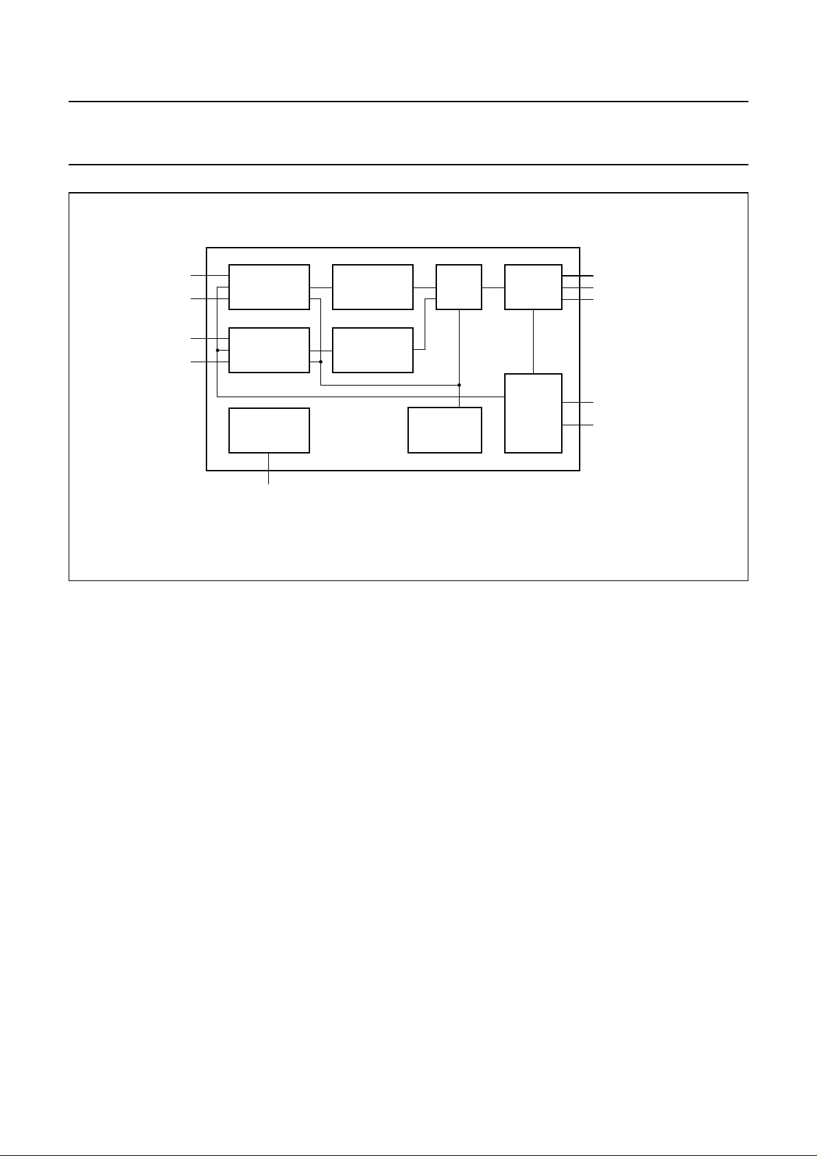
handbook, full pagewidth
+V
−V
+V
−V
O1
O1
O2
O2
ADC1
ADC2
DECIMATION
FILTER
DECIMATION
FILTER
ALU SPI CLK
data
CS
RESET
reset
UZZ9001
Fig.1 Block diagram.
The following list gives a short description of the relevant
block functions:
1. The ADC block contains two Sigma Delta AD
converters, sensor offset correction circuitry and the
circuitry required for the sensitivity and offset
adjustment of the chip output voltage curve.
2. Two digital low pass decimation filters convert the low
resolution high speed bit stream coming from the ADC
Sigma Delta converters into a low speed digital word.
3. The ALU block derives an angle value from the two
digital inputs using the CORDIC algorithm.
4. The SPI converts the output of the ALU block to a SPI
compatible 16 bit word.
5. The CONTROL block provides the clock and the
control signals for the chip.
6. The RESET block supplies a reset signal during
power-up and power-down when the power supply is
below a certain value.
7. The Oscillator unit generates the master clock.
CONTROL
OSCILLATOR
MHB698
DATA-CLK
SMODE
Serial Peripheral interface (SPI)
The UZZ9001 provides an interface to SPI compatible
devices, and as a slave node functions in one operational
mode only. For Motorola SPI devices, this mode is
selected by setting CPHA to 1 and CPOL to 1. In this
transfer mode, data bits are sampled by the master using
the leading edge of the clock as shown in Figure 2. The
falling edge indicates that the next data bit has to be
provided by the slave device (shift operation).
Anadvantageofthis mode is that the CS input toggles only
once between every two sensor data bytes (see Fig.3).
Data transmission can be stopped by the user at any time.
The leading edge of the CS input initialises the SPI shift
register allowing the start ofa complete new transmission.
Ifthe CS line isheld active low duringstop of transmission,
resumption of transmission can be made without loss of
data
2000 Nov 27 5
Page 6

Philips Semiconductors Product specification
Sensor Conditioning Electronic UZZ9001
handbook, full pagewidth
CS
1
2
5
CLK
3
10
8
DATA
(1) Not defined data, normally LSB of character previously transmitted.
4
MSB-OUTnote1
Fig.2 UZZ9001 SPI timing.
Table 1 SPI-Timing
DIAGRAM
NUMBER
1 cycle time t
2 enable lead time t
3 enable lag time t
4 clock high time t
5 clock low time t
8 access time t
9 disable time t
10 data valid time
PARAMETER SYMBOL MIN. MAX. UNIT REMARKS/TEST CONDITIONS
cyc
lead
lag
clk_high
clk_low
acc
dis
t
v
(after clock edge)
11 data hold time
t
h
(output, after clock edge)
operating frequency f
transmission delay
op
t
delay
(time between the
leading edge of CS until
the next falling edge)
9
LSB-OUTBits 6-1
1110
MHB699
1 −µs
15 − ns determined by master module
15 − ns determined by master module
100 − ns determined by master module
100 − ns determined by master module
0 20 ns time to data active from fixed V
state
− 25 ns hold time to fixed VSS state
− 40 ns with 100 pF on all SPI pins
5 − ns
− 1 MHz
1.2 −µs
SS
2000 Nov 27 6
Page 7

Philips Semiconductors Product specification
Sensor Conditioning Electronic UZZ9001
handbook, full pagewidth
DATA
CS
sensor byte 2 sensor byte 1
Fig.3 CS Line timing.
Sensor signal coding
Thesensorsignalcomprises 14 bits (D13 to D0) as shown
in Fig.4. Bits D12 to D0 are used for the coding of the
angle while D0 is reserved to indicate error and diagnostic
conditionsasdefinedbelow.The14data bitsare arranged
in 2 Bytes. D13 is the MSB of the sensor signal and D0 is
the LSB of the sensor signal. Byte 2, which is sent first,
contains data bits D13 to D7 and additionally the parity bit
P2 which is included for the recognition of interrupted
messages. P2 gives the ODD parity of data bits D13 to D7
and has to be evaluated by the master module.Similarly,
Byte 1 comprises data bits D6 to D0 and parity bit P1,
which gives the ODD parity of data bits D6 to D0. The
internal coding of angle values is as follows:
00 0000 0000 0000
=0°, 180°
B
MHB700
The error and diagnostic conditions are indicated by
D13 = 1 (active high). In an error situation the last two bits
(D0 and D1) specify the errorcode (see Table 2). Allother
bits (D3 to D12) still showthe current measurementvalue,
but as the last two bits are lost for measurement
representation the resolution is reduced to 11 bit.
Table 2 Error and diagnostic cases coding
MEASUREMENT
D1 D0 CASE
VALUE
RELIABLE
0 0 no valid value presently
no
available due to RESET
0 1 magnet lost no
1 0 reserved −
1 1 reserved −
01 1111 1111 1111B=
D13 DO
2
13
180°
1–()
------------
13
2
179.978≈
During normal operation, bit D13 is active low. Each
increment represents an angle value
180°
α
of:
= 0.022°≈
------------
inc
handbook, full pagewidth
13
2
sensor byte 2 sensor byte 1
P2 D13 D12 D11 D10 D9 D8 D7 P1 D6 D5 D4 D3
MSB LSB
Fig.4 Sensor signal coding.
2000 Nov 27 7
D2 D1 D0
MHB701
Page 8

Philips Semiconductors Product specification
Sensor Conditioning Electronic UZZ9001
Magnet lost condition
If both offset corrected input signal of sensor 1 and
sensor 2 are below the lost magnet threshold then the
failure ‘Magnet lost’ is assumed.
Offset trimming
To achieve a linear output characteristic, it is necessary to
shift the offsets of the two input signals to the input stage
of the UZZ9001. For this reason a sensor offset
cancellation procedure has been implemented in the
UZZ9001 which is started by sending a special serial data
protocol to the UZZ9001. This trimming procedure is
required for both input signals.
handbook, full pagewidth
DATA_CLK
(input at pin 9)
start
condition
statusbit #
12345
Trim interface
The UZZ9001 trim mode serial interface consists of the
two terminals SMODE (pin 10) and DATA_CLK (pin 9).
The structure of this protocol is shown in Figure 5.
All signal levels of DATA_CLK and SMODEmust lie within
the ranges set out in Table 3. The protocol starts with
a falling edge at the SMODE, which must occur at a high
DATA_CLK level. The following five bits are used to code
the message sent to the UZZ9001. They are transferred
via the SMODE and are sampled with the rising edge of
the DATA_CLK. During the fifth high level output of
DATA_CLK (counted from the start condition onwards),
a rising edge must appear at the SMODE and the
DATA_CLK follows this with one more change to low level
in order to successfully complete the protocol.
stop
condition
SMODE
(input at pin 10)
T1
TOUT
(output at pin 22)
T0
MHB702
Fig.5 Protocol used to set UZZ9001 into trim mode.
Table 3 Definition of the trim interface signals
PARAMETER MIN. MAX. UNIT
low level of DATA_CLK, SMODE 0 5 %V
high level of DATA_CLK, SMODE 95 100 %V
rise and fall time of DATA_CLK and SMODE signal edges
8 − ns
(10 to 90% VDD) and (90 to 10% VDD)
DATA_CLK frequency 0.1 1 MHz
DD
DD
2000 Nov 27 8
Page 9

Philips Semiconductors Product specification
Sensor Conditioning Electronic UZZ9001
Table 4 Programming of trim modes
MODE
enter trim mode for sensor input channel 1 0 0 0 1 0
enter trim mode for sensor input channel 2 0 0 1 0 0
leave trim mode for either input channel 0 0 0 0 0
How to enter the trim mode
Details of voltage levels and timing of the status bits to be
transmitted to the UZZ9001 are given inTable 3. Note that
a complete protocol has to be sent before normal
operation can be resumed. The trim mode can also be
exitedbyresettingthedevice.Afterentering one of the trim
modes and provided there is a dynamic input signal there
will be a square wave output at the terminal T
Reset
In addition to the external reset pin (pin 6), the UZZ9001
provides an internal power-up/ power-down reset logic
which continuously monitors the supply voltage.When the
supply voltage increases and reaches a safe level, reset
becomesinactive and the device starts initialization.When
the supply voltage exceeds the safe voltage level, the
deviceisresetimmediately.Thisinternalresetlogiccanbe
over-ridden in all modes and at any time by applying an
external active high command to the RES input pin (pin 6)
in all modes and at any time. The reset pin RES (pin 6).
This pin is internally pulled to ground and therefore need
not be connected if the function is not required.
OUT
12345
Measurement dynamics
The UZZ9001 includes an on-chip RC Oscillator that
generates the clock for the whole device. Consequently,
no external clock supply is required for the measurement
system. The nominal clock frequency of the on-chip
oscillator is 4 MHz at room temperature. It varies with
temperature change. At −40 °C the clock frequency may
(pin 22).
decrease to 2.3 MHz. At higher temperatures however,
a frequency up to 5.7 MHzmay occur. Thisinfluences the
dynamics of measurements. From an application point of
view, two different effects have to be distinguished. The
system delay, which means how long it takes until a
changed input signal is recognized at the output, and the
measurement update rate. The system delay is mainly
caused by the settling time of the low pass decimation
filter, which depends on the maximum frequency content
(shape) of the input signals and the clock frequency. The
following maximum values can be expected for the entire
system delay. The measurement update rate, however, is
directly related to the oscillator frequency. At room
temperature, a new value is available every 0.26 ms.
When taking the entire temperature range into account,
update rates between 0.45 and 0.18 ms are possible.
(see Table 5)
STATUS BITS
2000 Nov 27 9
Page 10

Philips Semiconductors Product specification
Sensor Conditioning Electronic UZZ9001
Table 5 System delay and update rates of the UZZ9001
PARAMETER MIN. TYP. MAX. UNIT
System delay (time elapsed until 95% of the final value is reached)
max. signal frequency < 200 MHz −−0.6 ms
transients (step response) −−1.2 ms
Measurement update rate
−40 °C 0.45 −− ms
+25 °C (room temperature) − 0.26 − ms
+150 °C −−0.18 ms
APPLICATION INFORMATION
handbook, full pagewidth
3, 4
7, 8
V
DD
GND
2
6
1
5
KMZ41
(1) For test applications pin to be left unconnected.
+V
+V
O2
1
O1
2
V
SS
3
4
5
6
UZZ9001
7
(1)
8
9
10
11
(1)
12
−V
O1
24
−V
O2
23
(1)
22
21
20
19
18
17
16
15
14
13
1
2
3
Fig.6 UZZ9001 trim mode configuration.
OFFS1
1
2
OFFS2
3
CS (chip select)
C1
100 nF
CLK (clock in)
data out
ground
SPI
in/out
MHB703
2000 Nov 27 10
Page 11

Philips Semiconductors Product specification
Sensor Conditioning Electronic UZZ9001
PACKAGE OUTLINE
SO24: plastic small outline package; 24 leads; body width 7.5 mm
D
c
y
Z
24
pin 1 index
1
e
13
12
w M
b
p
SOT137-1
E
H
E
Q
A
2
A
1
L
p
L
detail X
(A )
A
X
v M
A
A
3
θ
0 5 10 mm
scale
DIMENSIONS (inch dimensions are derived from the original mm dimensions)
UNIT
mm
inches
Note
1. Plastic or metal protrusions of 0.15 mm maximum per side are not included.
A
max.
2.65
0.10
OUTLINE
VERSION
SOT137-1
A
0.30
0.10
0.012
0.004
A2A
1
2.45
2.25
0.096
0.089
IEC JEDEC EIAJ
075E05 MS-013
0.25
0.01
b
3
p
0.49
0.32
0.36
0.23
0.019
0.013
0.014
0.009
(1)E(1) (1)
cD
15.6
7.6
7.4
0.30
0.29
1.27
0.050
15.2
0.61
0.60
REFERENCES
2000 Nov 27 11
eHELLpQ
10.65
10.00
0.419
0.394
1.4
0.055
1.1
0.4
0.043
0.016
1.1
1.0
0.043
0.039
PROJECTION
0.25
0.25 0.1
0.01
0.01
EUROPEAN
ywv θ
Z
0.9
0.4
0.035
0.004
0.016
ISSUE DATE
97-05-22
99-12-27
o
8
o
0
Page 12

Philips Semiconductors Product specification
Sensor Conditioning Electronic UZZ9001
DATA SHEET STATUS
DATA SHEET STATUS
Objective specification Development This data sheet contains the design target or goal specifications for
Preliminary specification Qualification This data sheet contains preliminary data, and supplementary data will be
Product specification Production This data sheet contains final specifications. Philips Semiconductors
Note
1. Please consult the most recently issued data sheet before initiating or completing a design.
DEFINITIONS
Short-form specification The data in a short-form
specification is extracted from a full data sheet with the
same type number and title. For detailed information see
the relevant data sheet or data handbook.
Limiting values definition Limitingvalues given are in
accordance with the Absolute Maximum Rating System
(IEC 60134). Stress above one or more of the limiting
values may cause permanent damage to the device.
These are stress ratings only and operation of the device
attheseor at any other conditions abovethosegivenin the
Characteristics sections of the specification is not implied.
Exposure to limiting values for extended periods may
affect device reliability.
Application information Applications that are
described herein for any of these products are for
illustrative purposes only. Philips Semiconductors make
norepresentationorwarrantythatsuchapplicationswill be
suitable for the specified use without further testing or
modification.
PRODUCT
STATUS
DEFINITIONS
product development. Specification may change in any manner without
notice.
published at a later date. Philips Semiconductors reserves the right to
make changes at any time without notice in order to improve design and
supply the best possible product.
reserves the right to make changes at any time without notice in order to
improve design and supply the best possible product.
DISCLAIMERS
Life support applications These products are not
designed for use in life support appliances, devices, or
systems where malfunction of these products can
reasonably be expected toresult in personalinjury. Philips
Semiconductorscustomersusingorsellingtheseproducts
for use in such applications do so at their own risk and
agree to fully indemnify Philips Semiconductors for any
damages resulting from such application.
Right to make changes Philips Semiconductors
reserves the right to make changes, without notice, in the
products, including circuits, standard cells, and/or
software, described or contained herein in order to
improve design and/or performance. Philips
Semiconductors assumes no responsibility or liability for
theuseofany of these products, conveys no licence or title
under any patent, copyright, or mask work right to these
products,and makes no representations or warrantiesthat
these products are free from patent, copyright, or mask
work right infringement, unless otherwise specified.
(1)
2000 Nov 27 12
Page 13

Philips Semiconductors Product specification
Sensor Conditioning Electronic UZZ9001
NOTES
2000 Nov 27 13
Page 14

Philips Semiconductors Product specification
Sensor Conditioning Electronic UZZ9001
NOTES
2000 Nov 27 14
Page 15

Philips Semiconductors Product specification
Sensor Conditioning Electronic UZZ9001
NOTES
2000 Nov 27 15
Page 16

Philips Semiconductors – a w orldwide compan y
Argentina: see South America
Australia: 3 Figtree Drive, HOMEBUSH, NSW 2140,
Tel. +61 2 9704 8141, Fax. +61 2 9704 8139
Austria: Computerstr. 6, A-1101 WIEN, P.O. Box 213,
Tel. +43 1 60 101 1248, Fax. +43 1 60 101 1210
Belarus: Hotel Minsk Business Center, Bld. 3, r. 1211, Volodarski Str. 6,
220050 MINSK, Tel. +375 172 20 0733, Fax. +375 172 20 0773
Belgium: see The Netherlands
Brazil: see South America
Bulgaria: Philips Bulgaria Ltd., Energoproject, 15th floor,
51 James Bourchier Blvd., 1407 SOFIA,
Tel. +359 2 68 9211, Fax. +359 2 68 9102
Canada: PHILIPS SEMICONDUCTORS/COMPONENTS,
Tel. +1 800 234 7381, Fax. +1 800 943 0087
China/Hong Kong: 501 Hong Kong Industrial Technology Centre,
72 Tat Chee Avenue, Kowloon Tong, HONG KONG,
Tel. +852 2319 7888, Fax. +852 2319 7700
Colombia: see South America
Czech Republic: see Austria
Denmark: Sydhavnsgade 23, 1780 COPENHAGEN V,
Tel. +45 33 29 3333, Fax. +45 33 29 3905
Finland: Sinikalliontie 3, FIN-02630 ESPOO,
Tel. +358 9 615 800, Fax. +358 9 6158 0920
France: 51 Rue Carnot, BP317, 92156 SURESNES Cedex,
Tel. +33 1 4099 6161, Fax. +33 1 4099 6427
Germany: Hammerbrookstraße 69, D-20097 HAMBURG,
Tel. +49 40 2353 60, Fax. +49 40 2353 6300
Hungary: see Austria
India: Philips INDIA Ltd, Band Box Building, 2nd floor,
254-D, Dr. Annie Besant Road, Worli, MUMBAI 400 025,
Tel. +91 22 493 8541, Fax. +91 22 493 0966
Indonesia: PTPhilips Development Corporation,Semiconductors Division,
Gedung Philips, Jl. Buncit Raya Kav.99-100, JAKARTA 12510,
Tel. +62 21 794 0040 ext. 2501, Fax. +62 21 794 0080
Ireland: Newstead, Clonskeagh, DUBLIN 14,
Tel. +353 1 7640 000, Fax. +353 1 7640 200
Israel: RAPAC Electronics, 7 Kehilat Saloniki St, PO Box 18053,
TEL AVIV 61180, Tel. +972 3 645 0444, Fax. +972 3 649 1007
Italy: PHILIPS SEMICONDUCTORS, Via Casati,23 - 20052 MONZA (MI),
Tel. +39 039 203 6838, Fax +39 039 203 6800
Japan: Philips Bldg 13-37, Kohnan 2-chome, Minato-ku,
TOKYO 108-8507, Tel. +81 3 3740 5130, Fax. +81 3 3740 5057
Korea: Philips House, 260-199 Itaewon-dong, Yongsan-ku, SEOUL,
Tel. +82 2 709 1412, Fax. +82 2 709 1415
Malaysia: No. 76 Jalan Universiti, 46200 PETALING JAYA, SELANGOR,
Tel. +60 3 750 5214, Fax. +60 3 757 4880
Mexico: 5900 Gateway East, Suite 200, EL PASO, TEXAS 79905,
Tel. +9-5 800 234 7381, Fax +9-5 800 943 0087
Middle East: see Italy
Netherlands: Postbus 90050, 5600 PB EINDHOVEN, Bldg. VB,
Tel. +31 40 27 82785, Fax. +31 40 27 88399
New Zealand: 2 Wagener Place, C.P.O. Box 1041, AUCKLAND,
Tel. +64 9 849 4160, Fax. +64 9 849 7811
Norway: Box 1, Manglerud 0612, OSLO,
Tel. +47 22 74 8000, Fax. +47 22 74 8341
Pakistan: see Singapore
Philippines: Philips Semiconductors Philippines Inc.,
106 Valero St. Salcedo Village, P.O. Box 2108 MCC, MAKATI,
Metro MANILA, Tel. +63 2 816 6380, Fax. +63 2 817 3474
Poland: Al.Jerozolimskie 195 B, 02-222 WARSAW,
Tel. +48 22 5710 000, Fax. +48 22 5710 001
Portugal: see Spain
Romania: see Italy
Russia: Philips Russia, Ul. Usatcheva 35A, 119048 MOSCOW,
Tel. +7 095 755 6918, Fax. +7 095 755 6919
Singapore: Lorong 1, Toa Payoh, SINGAPORE 319762,
Tel. +65 350 2538, Fax. +65 251 6500
Slovakia: see Austria
Slovenia: see Italy
South Africa: S.A. PHILIPS Pty Ltd., 195-215 Main Road Martindale,
2092 JOHANNESBURG, P.O. Box 58088 Newville 2114,
Tel. +27 11 471 5401, Fax. +27 11 471 5398
South America: Al. Vicente Pinzon, 173, 6th floor,
04547-130 SÃO PAULO, SP, Brazil,
Tel. +55 11 821 2333, Fax. +55 11 821 2382
Spain: Balmes 22, 08007 BARCELONA,
Tel. +34 93 301 6312, Fax. +34 93 301 4107
Sweden: Kottbygatan 7, Akalla, S-16485 STOCKHOLM,
Tel. +46 8 5985 2000, Fax. +46 8 5985 2745
Switzerland: Allmendstrasse 140, CH-8027 ZÜRICH,
Tel. +41 1 488 2741 Fax. +41 1 488 3263
Taiwan: Philips Semiconductors, 5F, No. 96, Chien Kuo N. Rd., Sec. 1,
TAIPEI, Taiwan Tel. +886 2 2134 2451, Fax. +886 2 2134 2874
Thailand: PHILIPS ELECTRONICS (THAILAND) Ltd.,
60/14 MOO 11, Bangna Trad Road KM. 3, Bagna, BANGKOK 10260,
Tel. +66 2 361 7910, Fax. +66 2 398 3447
Turkey: Yukari Dudullu, Org. San. Blg., 2.Cad. Nr. 28 81260 Umraniye,
ISTANBUL, Tel. +90 216 522 1500, Fax. +90 216 522 1813
Ukraine: PHILIPS UKRAINE, 4 Patrice Lumumba str., Building B, Floor 7,
252042 KIEV, Tel. +380 44 264 2776, Fax. +380 44 268 0461
United Kingdom: Philips Semiconductors Ltd., 276 Bath Road, Hayes,
MIDDLESEX UB3 5BX, Tel. +44 208 730 5000, Fax. +44 208 754 8421
United States: 811 East Arques Avenue, SUNNYVALE, CA 94088-3409,
Tel. +1 800 234 7381, Fax. +1 800 943 0087
Uruguay: see South America
Vietnam: see Singapore
Yugoslavia: PHILIPS, Trg N. Pasica 5/v, 11000 BEOGRAD,
Tel. +381 11 3341 299, Fax.+381 11 3342 553
For all other countries apply to: Philips Semiconductors,
Marketing Communications, Building BE-p, P.O. Box 218, 5600 MD EINDHOVEN,
The Netherlands, Fax. +31 40 27 24825
© Philips Electronics N.V. SCA
All rights are reserved. Reproduction in whole or in part is prohibited without the prior written consent of the copyright owner.
The information presented in this document does not form part of any quotation or contract, is believed to be accurate and reliable and may be changed
without notice. No liability will be accepted by the publisher for any consequence of its use. Publication thereof does not convey nor imply any license
under patent- or other industrial or intellectual property rights.
2000
Internet: http://www.semiconductors.philips.com
70
Printed in The Netherlands 613520/02/pp16 Date of release: 2000 Nov 27 Document order number: 9397 750 07784
 Loading...