

Page 1

DISCRETE SEMICONDUCTORS
DATA SH EET
UZZ9000
Sensor Conditioning Electronic
Product specification
Supersedes data of 2000 May 19
2000 Nov 27
Page 2

Philips Semiconductors Product specification
Sensor Conditioning Electronic UZZ9000
FEATURES
• One chip fully integrated signal conditioning IC
• Accuracy better than 1° together with KMZ41 in 100°
angle range
• Temperature range from −40 to 150 °C
• Adjustable angle range
• Adjustable zero point.
GENERAL DESCRIPTION
The UZZ9000 is an integrated circuit that combines two
sinusoidal signals (sine and cosine) into one single linear
output signal. When used in conjunction with the
magnetoresistive sensor KMZ41 it provides a
measurement systemfor angles up to 180°. The UZZ9000
can also be used for other applications in which an angle
has to be calculated from a sine and a cosine signal.
A typical application would be any kind of resolver
application.
The two input signalsare convertedinto thedigital domain
with two separate AD-converters. A CORDIC algorithm
performsthe inverse tangenttransformation.Sincetoday’s
applications typically require analog output signals
(e.g. potentiometers), the resulting signal is transferred
back to the analog domain.
TheUZZ9000 enablesthe userto setboth the anglerange
and the zero point offset. Theseranges areset byexternal
voltage dividers.
PINNING
SYMBOL PIN DESCRIPTION
+V
+V
V
V
O2
O1
DD2
SS
1 sensor 2 positive differential input
2 sensor 1 positive differential input
3 digital supply voltage
4 digital ground
GND 5 analog ground
RST 6 reset of the digital part; note 1
TEST1 7 for production test; note 1
TEST2 8 note 2
DATA_CLK 9 trim-mode data-clock; note 1
SMODE 10 serial mode programmer; note 1
TEST3 11 note 2
V
OUT
12 output voltage
Var 13 angle-range input set
V
offin
14 offset input set
OFFS2 15 offset trimming input sensor 2
OFFS1 16 offset trimming input sensor 1
V
DDA
17 analog supply voltage
GND 18 analog ground
TEST4 19 for production test; note 1
TEST5 20 for production test; note 1
V
T
−V
−V
DD1
out
O2
O1
21 digital supply voltage
22 test output
23 sensor 2 negative differential input
24 sensor 1 negative differential input
Notes
1. Connected to ground.
2. Pin to be left unconnected.
QUICK REFERENCE DATA
SYMBOL PARAMETER CONDITIONS MIN. TYP. MAX. UNIT
V
DDA
V
DD1
V
DD2
I
CCtot
supply voltage note 1 4.5 5 5.5 V
supply voltage note 1 4.5 5 5.5 V
supply voltage note 1 4.5 5 5.5 V
total supply current − 13 15 mA
A angle range in 10° steps with KMZ41 30 − 180 deg
A accuracy with ideal input signal; range = 100°±0.45 −−deg
Note
1. V
DDA
, V
DD1
and V
must be connected to the same supply voltage.
DD2
2000 Nov 27 2
Page 3

Philips Semiconductors Product specification
Sensor Conditioning Electronic UZZ9000
LIMITING VALUES
In accordance with the Absolute Maximum Rating System (IEC 60134).
SYMBOL PARAMETER CONDITIONS MIN. MAX. UNIT
V
DDA
V
DD1
V
DD2
V
pin
T
stg
T
j
THERMAL CHARACTERISTICS
SYMBOL PARAMETER VALUE UNIT
R
th j-a
supply voltage −0.3 +6 V
supply voltage −0.3 +6 V
supply voltage −0.3 +6 V
voltage at all pins −0.3 V
DD
V
storage temperature −55 +150 °C
operating temperature 125 to 150 °C; max 200 hours −40 +150 °C
thermal resistance from junction to ambient 80 K/W
ESD SENSITIVITY
SYMBOL PARAMETER CONDITIONS VALUE UNIT
ESD ESD sensitivity human body model 2 kV
machine model ±150 V
2000 Nov 27 3
Page 4

Philips Semiconductors Product specification
Sensor Conditioning Electronic UZZ9000
ELECTRICAL CHARACTERISTICS
T
= −40 to +150 °C; VDD= 4.5 to 5.5 V; typical characteristics for T
amb
specified.
SYMBOL PARAMETER CONDITIONS MIN. TYP. MAX. UNIT
V
DDA
V
DD1
V
DD2
I
DD
(+V
)-(−VO) differential input voltage referred to V
O
f
ext
f
int
C
load
supply voltage 4.5 5 5.5 V
supply voltage 4.5 5 5.5 V
supply voltage 4.5 5 5.5 V
supply current without load − 10 15 mA
DD
common mode range referred to V
lost magnet threshold referred to V
DD
DD
external clock frequency for trim interface 0.1 − 1 MHz
internal clock frequency Tj= −40 to 150 °C 2.3 4 5.7 MHz
output load −−50 pF
with series resistance
>300 Ω
V
reset
switchingvoltagethreshold
for power on/off
between falling and
rising V
DD
hysteresis − 0.3 −
V
out
V
d
output voltage range for
valid ranges
lower bound 5 − 6% V
upper bound 94 − 95 % V
diagnostic area for irregular input
signal
A accuracy with ideal input signal;
range = 100°
Res resolution range = 100° 0.1 −−degree
t
on
t
r
V
LM
power up time −−20 ms
response time to 95% of final value − 0.7 1.2 ms
sensor voltage lost magnet threshold 12 15 20 mV
=25°C and VDD= 5 V unless otherwise
amb
±6.6 −±28 mV/V
490 − 510 mV/V
− 3 − mV/V
−−200 nF
2.8 − 4.5 V
DD
DD
0 − 4% V
96 − 100 % V
DD
DD
±0.45 −−degree
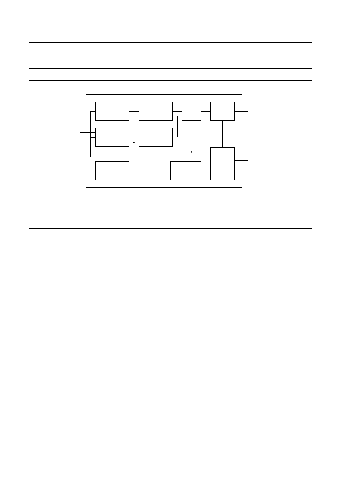
FUNCTIONAL DESCRIPTION
The UZZ9000is a mixedsignal IC for angle measurement
systems. The UZZ9000 has been designed for the double
sensor KMZ41. It combines two analog signals (sine and
cosine) into a linear output signal. The analog
measurement signals on the IC input are converted to
digital data by two ADC’s. Each ADC is a Sigma-Delta
modulator employing a 4th order continuous time
architecture with an over-sampling ratio of 128 to achieve
high resolution. The converteroutput isa digitalbit-stream
with an over-sampling frequency of typically 500 kHz.
The bit-stream is fed into a decimation filter which
2000 Nov 27 4
performs both low pass filtering and down-sampling. The
IC has twoinput channels each of which has its own ADC
and decimationfilter. The twodecimation filter outputsare
15-bit digital words at a lower frequency of typically
3.9 kHz which is the typical sampling frequency of the
sensor system. The digital representations of the two
signals arethen used to calculatethe current angleby the
ALU. This calculation is carried out using the so-called
CORDIC algorithm. The angle is represented by a 13-bit
resolution. A DAC converts the digital signal back to the
analog domain.
Page 5
Philips Semiconductors Product specification
Sensor Conditioning Electronic UZZ9000
handbook, full pagewidth
+V
−V
+V
−V
O1
O1
O2
O2
ADC1
ADC2
RESET
DECIMATION
FILTER
DECIMATION
FILTER
UZZ9000
ALU DAC output
CONTROL
OSCILLATOR
angle range
offset
DATA-CLK
SMODE
reset
Fig.1 Block diagram.
The following list gives a short description of the relevant
block functions:
1. The ADC block contains two Sigma Delta AD
converters, sensor offset correction circuitry and the
circuitry required for the sensitivity and offset
adjustment of the chip output voltage curve.
2. The decimation filter block comprises two digital low
pass decimation filtersconvert the low resolution high
speed bit stream output from the ADC’s into a low
speed digital word.
3. The ALU block derives an angle value from the two
digital inputs using the CORDIC algorithm.
4. The DAC converts the output of the ALU block to an
analog signal.
5. The CONTROL block provides the clock and the
control signals for the chip.
6. The RESET block supplies a reset signal during
power-up and power-down when the power supply is
below a certain value.
7. The Oscillator generates the master clock.
MHB694
Angle range selection
In order to accommodate varying applications, both the
mechanical input angular range of the UZZ9000 and the
zeropoint oftheoutput curveareuser programmable.This
section describes how to select a desired mode.
The output curve is adjusted by changing the angular
range asshown inFig.2. Without anyzero pointoffset, the
ramp-up starts at mechanical 0° (α1=0°). When using a
KMZ41 sensor, the maximum angular range ∆α
is 0° to 180°. For the UZZ9000, smaller angular ranges
can be set. In this case, α2 becomes smaller than 180°
and the output curve is clipped at this position. The
location of discontinuity XD (change from lower to upper
clipping area) depends on the adjusted range and can be
calculated as follows:
180°∆α–
∆α
X
D
+=
-------------------------2
Inorder tocompensate fortolerances, thezero point ofthe
output curve can be shifted by ±5˚ in steps of 0.5°. The
effect of this measure is shown in Fig.3. Now α1 is no
longer identicalwith mechanical 0˚,but with the zero point
shift X
. Consequently, the location of discontinuity X
off
D
can be calculated as follows:
2000 Nov 27 5
X
Dxoff
∆α+
180°∆α–
+=
-------------------------2
Page 6

Philips Semiconductors Product specification
Sensor Conditioning Electronic UZZ9000
handbook, full pagewidth
V
out
When using MR sensors (KMZ41), the signalperiod is0˚ to 180˚as
the signals are proportional to sin2α and cos2α.
Fig.2 Output curve for different angular ranges.
α1
∆α
α2
∆β ∆β
180°(360°)0°
α/°
MHB695
handbook, full pagewidth
V
out
When using MR sensors (KMZ41), the signalperiod is0˚ to 180˚as
the signals are proportional to sin2α and cos2α.
α1
X
off
Fig.3 Output curve for different angular ranges including a zero point offset.
2000 Nov 27 6
∆α
α2
∆β ∆β
180°(360°)0°
α/°
MHB696
Page 7

Philips Semiconductors Product specification
Sensor Conditioning Electronic UZZ9000
Angle range setting
To select one of 16 different angular ranges, an external
voltage (see Table 1) must be applied to pin 13 of the
UZZ9000 (Var). During the ICs initialisation phase, which
directly follows power-on reset or an external reset, this
voltage isread and thenconverted into the digital domain.
The digitalvalue is stored until thenext reset stateoccurs.
Consequently, the angular range cannot be changed
during normal operation but is still fixed after initialisation
phase. Note that thevoltage at pin 13 must be ratiometric
toV
andalso stableover temperatureand lifetime. This
DDA
is ensured, for instance, when providingthis voltage via a
(trimmable) resistor divider connected to V
DDA
, which is
the analog supply of the UZZ9000. The following defines
the % value of the supply voltage V
that must be
DDA
supplied to pin 13 to select a certain range. When using
the 30° angular range, a constant zero point offset of 15°
is added. Consequently, when using the 30° range, the
zeropoint offsetcan beprogrammed between10° and20°
only (see Zero point offset setting).
Table 1 Definition of voltages to set UZZ9000 angular
ranges
ANGULAR
RANGE
(°)
0 to 30 33.47 33.73 33.99 V
0 to 40 35.69 35.95 36.21 V
0 to 50 37.91 38.17 38.43 V
0 to 60 40.14 40.40 40.66 V
0 to 70 42.36 42.62 42.88 V
0 to 80 44.58 44.84 45.10 V
0 to 90 46.80 47.06 47.32 V
0 to 100 49.02 49.28 49.54 V
0 to 110 51.25 51.51 51.77 V
0 to 120 53.47 53.73 53.99 V
0 to 130 55.69 55.95 56.21 V
0 to 140 57.91 58.17 58.43 V
0 to 150 60.13 60.39 60.65 V
0 to 160 62.36 62.62 62.88 V
0 to 170 64.58 64.84 65.10 V
0 to 180 66.80 67.06 67.32 V
MIN.
(%)
NOM.
(%)
MAX.
(%)
UNIT
(%)
DDA
DDA
DDA
DDA
DDA
DDA
DDA
DDA
DDA
DDA
DDA
DDA
DDA
DDA
DDA
DDA
Zero point offset setting
To adjustthe zeropoint offset orto set it to 0°,an external
voltage has to be applied to the UZZ9000 at pin 14
(VOFFIN). The function is similar to that described
previously. After reset the voltage is read, converted into
the digital domain andthen storeduntil anotherreset state
occurs. Consequently, the zero point offset cannot be
adjusted without a reset. It is recommended to use a
resistordivider connectedtoV
togenerate thisvoltage.
DDA
Table 2 defines the allowed voltage ranges as a
percentage of the supply V
DDA
.
Table 2 Definition of voltages to set a certain zero point
offset
ZERO
POINT
OFFSET
MIN.
(%)
NOM.
(%)
MAX.
(%)
UNIT
(%)
(°)
−5 33.47 33.73 33.99 V
−4.5° 35.14 35.40 35.66 V
−4° 36.80 37.06 37.32 V
−3.5° 38.47 38.73 38.99 V
−3° 40.13 40.39 40.65 V
−2.5° 41.80 42.06 42.32 V
−2° 43.47 43.73 43.99 V
−1.5 ° 45.13 45.39 45.65 V
−1° 46.80 47.06 47.32 V
−0.5° 48.60 48.72 48.98 V
0° 50.13 50.39 50.65 V
0.5° 51.80 52.06 52.32 V
1° 53.46 53.72 53.98 V
1.5° 64.58 55.39 55.65 V
2° 56.79 57.05 57.31 V
2.5° 58.46 58.72 58.98 V
3° 60.13 60.39 60.65 V
3.5° 61.79 62.05 62.31 V
4° 63.46 63.72 63.98 V
4.5° 65.12 65.38 65.64 V
5° 66.79 67.05 67.31 V
DDA
DDA
DDA
DDA
DDA
DDA
DDA
DDA
DDA
DDA
DDA
DDA
DDA
DDA
DDA
DDA
DDA
DDA
DDA
DDA
DDA
Offset trimming
To achievea linear outputcharacteristic, it is necessary to
adapt theoffsets of the two inputsignals to theinput stage
of the UZZ9000. For this reason a sensor offset
cancellation procedure has been implemented in the
UZZ9000 whichis started by sendinga special serial data
protocol to the UZZ9000. This trimming procedure is
required for both input signals.
2000 Nov 27 7
Page 8

Philips Semiconductors Product specification
Sensor Conditioning Electronic UZZ9000
Trim interface
The serial interface used to switch the UZZ9000 into trim
mode consists of the two terminals SMODE (pin 10) and
DATA_CLK (pin 9).The structureof this protocolis shown
in Fig.4.
All signal levels at DATA_CLK and SMODE must be
selected according to the requirements listed in Table 3.
The following points must be taken into account with
regard to the asynchronous protocol.
The protocol starts with a falling edge at the SMODE,
handbook, full pagewidth
DATA_CLK
(input at pin 9)
SMODE
(input at pin 10)
TOUT
(output at pin 22)
start
condition
status bit
12345
whichmust occurata highDATA_CLKlevel. Thefollowing
five bits are used to code the message sent to the
UZZ9000. They are transferred via the SMODE and are
sampledwith therisingedge oftheDATA_CLK. Duringthe
fifthhigh leveloutputof DATA_CLK(countedfrom thestart
condition onwards), a rising edge must appear at the
SMODE and the DATA_CLK follows this with one more
change to low level in order to successfully complete the
protocol.
stop
condition
T1
T0
MHB697
Fig.4 Protocol used to set UZZ9000 into trim mode.
Table 3 Definition of the trim interface signals
PARAMETER MIN. NOM. MAX. UNIT
UZZ9000 supply voltage 4.5 5 5.5 V
low level of DATA_CLK, SMODE 0 − 5%V
high level of DATA_CLK, SMODE 95 − 100 %V
rise and fall time of DATA_CLK and SMODE signal
8 −−
edges (10 to 90% VDD) and (90 to 10% VDD)
DD
DD
ns
DATA_CLK frequency 0.1 − 1 MHz
How to enter the trim mode
The status bits to be transmitted to the UZZ9000 are shown in Table 4. Note that a complete protocol has to be sent
before normal operation can be resumed. The trim mode can also be exited by resetting the device. After entering one
of the trim modes and provided there is a dynamic input signal, a square wave output is visible at the terminal T
OUT
(pin 22).
2000 Nov 27 8
Page 9

Philips Semiconductors Product specification
Sensor Conditioning Electronic UZZ9000
Table 4 Programming of trim modes
MODE
STATUS BITS
12345
enter trim mode for sensor input channel 1 0 0 0 1 0
enter trim mode for sensor input channel 2 0 0 1 0 0
leave trim mode for either input channel 0 0 0 0 0
Reset
In addition to the external reset pin (pin 6), the UZZ9001
provides an internal power-up/ power-down reset logic
which continuously monitors thesupply voltage.When the
supply voltage increases and reaches a safe level, reset
becomesinactive andthe devicestartsinitialization. When
the supply voltage exceeds the safe voltage level, the
deviceis resetimmediately. Thisinternalreset logiccan be
over-ridden by the external pin RES (pin 6) in all modes
and at any time. The reset pin RES (pin 6) is active when
in the high position. It is internally pulled to ground and
therefore need not be connected if the function is not
required.
the device enters into the diagnostic area if VDD is
disconnected, but not if VSS is disconnected. Similarly, if
the load is apull-up resistor, then the device will enter the
diagnostic area if VSS is disconnected, but not if VDD is
disconnected.It isnot necessary toconnect anoutputload
to the UZZ9000. After recovering from short circuit to
ground or supply voltage, the chip returns undamaged to
the normal operation mode. There is no time limitation
regarding short circuit of V
OUT
.
Measurement dynamics
The UZZ9000 includes an on-chip RC Oscillator that
generates the clock for the whole device. Consequently,
no external clock supply is required for the measurement
Diagnostic
The UZZ9000 providespowerful diagnostics features that
allow theuser torecognize certain failuresof thedevice or
system. A failure will occur when the output voltage V
OUT
either rises above or falls below the normal operation
range.Either oneof thediagnostic areas isreached during
any of the following conditions
1. Short circuit between V
2. Short circuit between V
and GND (R < 1 Ω).
OUT
and VDD (R<1Ω).
OUT
3. Disconnection of VDD when the load is pulled down.
4. Disconnection of GND when the load is pulled up.
5. Invalid input signal from the sensor, e.g.Magnet Lost.
Thisfailure isassumed when theoffset correctedinput
signal of sensor 1 and sensor 2 is below ±15 mV.
The internal pull-up and pull-down resistors in the output
buffer block ensure that V
will be pulled to one of the
OUT
power supplies when the other supply is disconnected so
V
reaches thediagnostic region evenwhen there isno
OUT
system. The nominal clock frequency of the on-chip
oscillator is 4 MHz at room temperature. It varies with
temperature change. At −40 °C the clock frequency may
decrease to 2.3 MHz. At higher temperatures however, a
frequency up to 5.7 MHz maybe reached.This influences
the dynamics of measurements.From anapplication point
of view,two different effectshave to be distinguished: The
system delay, which means how long it takes until a
changed input signal is recognized at the output, and the
measurement update rate. The system delay is mainly
caused by the settling time of the low pass decimation
filter, which depends on the maximum frequency content
(shape) of the input signals and the clock frequency. The
following maximum values can be expected for the entire
system delay. The measurement update rate, however,is
directly related to the oscillator frequency. At room
temperature, a new value is available every 0.26 ms.
When taking the entire temperature range into account,
updaterates between0.45 and 0.18 msare possible.(see
Table 5).
outputload. Ifthe externalload is apull-downresistor, then
2000 Nov 27 9
Page 10

Philips Semiconductors Product specification
Sensor Conditioning Electronic UZZ9000
Table 5 System delay and update rates of the UZZ9000
PARAMETER MIN. TYP. MAX. UNIT
system delay (time elapsed until 95% of the final value is reached)
max. signal frequency < 200 MHz −−0.6 ms
transients (step response) −−1.2 ms
measurement update rate
−40 °C 0.45 −− ms
25 °C (room temperature) − 0.26 − ms
150 °C −−0.18 ms
2000 Nov 27 10
Page 11

Philips Semiconductors Product specification
Sensor Conditioning Electronic UZZ9000
PACKAGE OUTLINE
SO24: plastic small outline package; 24 leads; body width 7.5 mm
D
c
y
Z
24
pin 1 index
1
e
13
12
w M
b
p
SOT137-1
E
H
E
Q
A
2
A
1
L
p
L
detail X
(A )
A
X
v M
A
A
3
θ
0 5 10 mm
scale
DIMENSIONS (inch dimensions are derived from the original mm dimensions)
UNIT
mm
inches
Note
1. Plastic or metal protrusions of 0.15 mm maximum per side are not included.
A
max.
2.65
0.10
OUTLINE
VERSION
SOT137-1
A1A2A
0.30
2.45
0.10
2.25
0.012
0.096
0.004
0.089
IEC JEDEC EIAJ
075E05 MS-013
0.25
0.01
b
3
p
0.49
0.32
0.36
0.23
0.019
0.013
0.014
0.009
(1)E(1) (1)
cD
15.6
7.6
7.4
0.30
0.29
1.27
0.050
15.2
0.61
0.60
REFERENCES
2000 Nov 27 11
eHELLpQ
10.65
10.00
0.419
0.394
1.4
0.055
1.1
0.4
0.043
0.016
1.1
1.0
0.043
0.039
PROJECTION
0.25
0.25 0.1
0.01
0.01
EUROPEAN
ywv θ
Z
0.9
0.4
0.035
0.004
0.016
ISSUE DATE
97-05-22
99-12-27
o
8
o
0
Page 12

Philips Semiconductors Product specification
Sensor Conditioning Electronic UZZ9000
DATA SHEET STATUS
DATA SHEET STATUS
Objective specification Development This data sheet contains the design target or goal specifications for
Preliminary specification Qualification This datasheet contains preliminary data, andsupplementary datawill be
Product specification Production This data sheet contains final specifications. Philips Semiconductors
Note
1. Please consult the most recently issued data sheet before initiating or completing a design.
DEFINITIONS
Short-form specification The data in a short-form
specification is extracted from a full data sheet with the
same type number and title. For detailed information see
the relevant data sheet or data handbook.
Limiting valuesdefinition Limiting values givenare in
accordance with the Absolute Maximum Rating System
(IEC 60134). Stress above one or more of the limiting
values may cause permanent damage to the device.
These are stress ratings only and operation of the device
atthese orat any otherconditions abovethosegiven inthe
Characteristics sectionsof the specification isnot implied.
Exposure to limiting values for extended periods may
affect device reliability.
Application information Applications that are
described herein for any of these products are for
illustrative purposes only. Philips Semiconductors make
norepresentation orwarranty thatsuchapplications willbe
suitable for the specified use without further testing or
modification.
PRODUCT
STATUS
DEFINITIONS
product development. Specification may change in any manner without
notice.
published at a later date. Philips Semiconductors reserves the right to
make changes at any time without notice in order to improve design and
supply the best possible product.
reserves the right to make changes at any time without notice in order to
improve design and supply the best possible product.
DISCLAIMERS
Life support applications These products are not
designed for use in life support appliances, devices, or
systems where malfunction of these products can
reasonably be expected to result in personal injury.Philips
Semiconductorscustomers usingor sellingtheseproducts
for use in such applications do so at their own risk and
agree to fully indemnify Philips Semiconductors for any
damages resulting from such application.
Right to make changes Philips Semiconductors
reserves the right to make changes, without notice, in the
products, including circuits, standard cells, and/or
software, described or contained herein in order to
improve design and/or performance. Philips
Semiconductors assumes no responsibility or liability for
theuse ofanyof theseproducts,conveys nolicenceor title
under any patent, copyright, or mask work right to these
products,and makesno representationsor warrantiesthat
these products are free from patent, copyright, or mask
work right infringement, unless otherwise specified.
(1)
2000 Nov 27 12
Page 13

Philips Semiconductors Product specification
Sensor Conditioning Electronic UZZ9000
NOTES
2000 Nov 27 13
Page 14

Philips Semiconductors Product specification
Sensor Conditioning Electronic UZZ9000
NOTES
2000 Nov 27 14
Page 15

Philips Semiconductors Product specification
Sensor Conditioning Electronic UZZ9000
NOTES
2000 Nov 27 15
Page 16

Philips Semiconductors – a w orldwide compan y
Argentina: see South America
Australia: 3 Figtree Drive, HOMEBUSH, NSW 2140,
Tel. +61 2 9704 8141, Fax. +61 2 9704 8139
Austria: Computerstr. 6, A-1101 WIEN, P.O. Box 213,
Tel. +43 1 60 101 1248, Fax. +43 1 60 101 1210
Belarus: Hotel Minsk Business Center, Bld. 3, r. 1211, Volodarski Str. 6,
220050 MINSK, Tel. +375 172 20 0733, Fax. +375 172 20 0773
Belgium: see The Netherlands
Brazil: seeSouth America
Bulgaria: Philips Bulgaria Ltd., Energoproject, 15thfloor,
51 James Bourchier Blvd., 1407 SOFIA,
Tel. +359 2 68 9211, Fax. +359 2 68 9102
Canada: PHILIPS SEMICONDUCTORS/COMPONENTS,
Tel. +1 800 234 7381, Fax. +1 800 943 0087
China/Hong Kong: 501 Hong Kong Industrial Technology Centre,
72 Tat Chee Avenue, Kowloon Tong, HONG KONG,
Tel. +852 2319 7888, Fax. +852 2319 7700
Colombia: see South America
Czech Republic: see Austria
Denmark: Sydhavnsgade 23, 1780 COPENHAGEN V,
Tel. +45 33 29 3333, Fax. +45 33 29 3905
Finland: Sinikalliontie 3, FIN-02630 ESPOO,
Tel. +358 9 615 800, Fax. +358 9 6158 0920
France: 51 Rue Carnot, BP317, 92156 SURESNES Cedex,
Tel. +33 1 4099 6161, Fax. +33 1 4099 6427
Germany: Hammerbrookstraße 69, D-20097 HAMBURG,
Tel. +49 40 2353 60, Fax. +49 40 2353 6300
Hungary: seeAustria
India: Philips INDIA Ltd, Band Box Building, 2nd floor,
254-D, Dr. Annie Besant Road, Worli, MUMBAI 400 025,
Tel. +91 22 493 8541, Fax. +91 22 493 0966
Indonesia: PTPhilipsDevelopment Corporation, Semiconductors Division,
Gedung Philips, Jl. Buncit Raya Kav.99-100, JAKARTA 12510,
Tel. +62 21 794 0040 ext. 2501, Fax. +62 21 794 0080
Ireland: Newstead, Clonskeagh, DUBLIN 14,
Tel. +353 1 7640 000, Fax. +353 1 7640 200
Israel: RAPAC Electronics, 7 Kehilat Saloniki St, PO Box 18053,
TEL AVIV 61180, Tel. +972 3 645 0444, Fax. +972 3 649 1007
Italy: PHILIPS SEMICONDUCTORS, ViaCasati, 23 - 20052 MONZA (MI),
Tel. +39 039 203 6838, Fax +39 039 203 6800
Japan: Philips Bldg 13-37, Kohnan 2-chome, Minato-ku,
TOKYO 108-8507, Tel. +81 3 3740 5130, Fax. +81 3 3740 5057
Korea: Philips House, 260-199 Itaewon-dong, Yongsan-ku, SEOUL,
Tel. +82 2 709 1412, Fax. +82 2 709 1415
Malaysia: No. 76 Jalan Universiti, 46200 PETALING JAYA, SELANGOR,
Tel. +60 3 750 5214, Fax. +60 3 757 4880
Mexico: 5900 Gateway East, Suite 200, EL PASO, TEXAS 79905,
Tel. +9-5 800 234 7381, Fax +9-5 800 943 0087
Middle East: see Italy
Netherlands: Postbus 90050, 5600 PB EINDHOVEN, Bldg. VB,
Tel. +31 40 27 82785, Fax. +31 40 27 88399
New Zealand: 2 Wagener Place, C.P.O. Box 1041, AUCKLAND,
Tel. +64 9 849 4160, Fax. +64 9 849 7811
Norway: Box 1, Manglerud 0612, OSLO,
Tel. +47 22 74 8000, Fax. +47 22 74 8341
Pakistan: see Singapore
Philippines: Philips Semiconductors Philippines Inc.,
106 Valero St. Salcedo Village, P.O. Box 2108 MCC, MAKATI,
Metro MANILA, Tel. +63 2 816 6380, Fax. +63 2 817 3474
Poland: Al.Jerozolimskie 195 B, 02-222 WARSAW,
Tel. +48 22 5710 000, Fax. +48 22 5710 001
Portugal: see Spain
Romania: see Italy
Russia: Philips Russia, Ul. Usatcheva 35A, 119048 MOSCOW,
Tel. +7 095 755 6918, Fax. +7 095 755 6919
Singapore: Lorong 1, Toa Payoh, SINGAPORE 319762,
Tel. +65 350 2538, Fax. +65 251 6500
Slovakia: see Austria
Slovenia: see Italy
South Africa: S.A. PHILIPS Pty Ltd., 195-215 Main Road Martindale,
2092 JOHANNESBURG, P.O. Box 58088 Newville 2114,
Tel. +27 11 471 5401, Fax. +27 11 471 5398
South America: Al. Vicente Pinzon, 173, 6th floor,
04547-130 SÃO PAULO, SP, Brazil,
Tel. +55 11 821 2333, Fax. +55 11 821 2382
Spain: Balmes 22, 08007 BARCELONA,
Tel. +34 93 301 6312, Fax. +34 93 301 4107
Sweden: Kottbygatan 7, Akalla, S-16485 STOCKHOLM,
Tel. +46 8 5985 2000, Fax. +46 8 5985 2745
Switzerland: Allmendstrasse 140, CH-8027 ZÜRICH,
Tel. +41 1 488 2741 Fax. +41 1 488 3263
Taiwan: Philips Semiconductors, 5F, No. 96, Chien Kuo N. Rd., Sec. 1,
TAIPEI, Taiwan Tel. +886 2 2134 2451, Fax. +886 2 2134 2874
Thailand: PHILIPS ELECTRONICS (THAILAND) Ltd.,
60/14 MOO 11, Bangna Trad Road KM. 3, Bagna, BANGKOK 10260,
Tel. +66 2 361 7910, Fax. +66 2 398 3447
Turkey: Yukari Dudullu, Org. San. Blg., 2.Cad. Nr. 28 81260 Umraniye,
ISTANBUL, Tel. +90 216 522 1500, Fax. +90 216 522 1813
Ukraine: PHILIPS UKRAINE, 4 Patrice Lumumba str., Building B, Floor 7,
252042 KIEV, Tel. +380 44 264 2776, Fax. +380 44 268 0461
United Kingdom: Philips Semiconductors Ltd., 276 Bath Road, Hayes,
MIDDLESEX UB3 5BX, Tel. +44 208 730 5000, Fax. +44 208 754 8421
United States: 811 East Arques Avenue, SUNNYVALE, CA 94088-3409,
Tel. +1 800 234 7381, Fax. +1 800 943 0087
Uruguay: see South America
Vietnam: see Singapore
Yugoslavia: PHILIPS, Trg N. Pasica 5/v, 11000 BEOGRAD,
Tel. +381 11 3341 299, Fax.+381 11 3342 553
For all other countries apply to: Philips Semiconductors,
Marketing Communications, Building BE-p, P.O. Box 218, 5600 MD EINDHOVEN,
The Netherlands, Fax. +31 40 27 24825
© Philips Electronics N.V. SCA
All rights are reserved. Reproduction in whole or in part is prohibited without the prior written consent of the copyright owner.
The information presented in thisdocument does not form partof any quotation or contract, is believed to be accurate and reliable and may be changed
without notice. No liability will be accepted by the publisher for any consequence of its use. Publication thereof does not convey nor imply any license
under patent- or other industrial or intellectual property rights.
2000
Internet: http://www.semiconductors.philips.com
70
Printed in The Netherlands 613520/04/pp16 Date of release: 2000 Nov27 Document order number: 9397 750 07783
 Loading...