

Page 1
UTC MC34072 LINEAR INTEGRATED CIRCUIT
HIGH SLEW RATE, WIDE
BANDWIDTH, SINGLE SUPPLY
OPERATIONAL AMPLIFIERS
DESCRIPTION
The UTC MC34072 offer 4.5MHz of gain bandwidth
product, 13V/µs slew rate and fast setting time without
the use of JFET device technology. Although it can be
operated from split supplies, it is particularly suited for
single supply operation, since the common mode input
voltage range includes ground potential (VEE). With A
Darlington input stage, it exhibits high input resistance,
low input offset voltage and high gain. The all NPN
output stage, characterized by no deadband crossover
distortion and large output voltage swing, provides
high capacitance drive capability, excellent phase and
gain margins, low open loop high frequency output
impedance and symmetrical source/sink AC frequency
response.
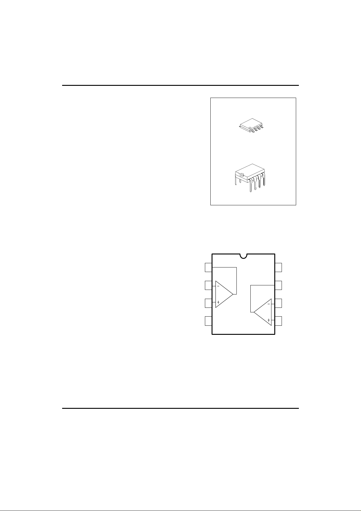
SOP-8
DIP-8
FEATURES
*Wide bandwidth: 4.5 MHz
*High slew rate: 13V/µs
*Fast settling time:1.1µs to 0.1%
*Wide single supply operation: 3.0V to 44V
*Wide input common mode voltage range:
Includes Ground (VEE)
*Low input offset voltage: 3.0mV maximum
*Large output voltage swing: -14.7V to +14V
(with +-15V supplies)
*Large Capacitance Drive Capability:0 pF to 10,000 pF
*Low total harmonic distortion: 0.02%
*Excellent phase margin: 60°
*Excellent gain margin: 12dB
*Output short circuit protection
*ESD Diodes/Clamps provide input protection
PING CONFIGURATIONS
Output 1
1
Input 1
2
3
VEE
4
8
7
6
5
VCC
Output 2
Input 2Input 1
Input 2
UTC UNISONIC TECHNOLOGIES CO., LTD. 1
QW-R105-007,A
Page 2
UTC MC34072 LINEAR INTEGRATED CIRCUIT
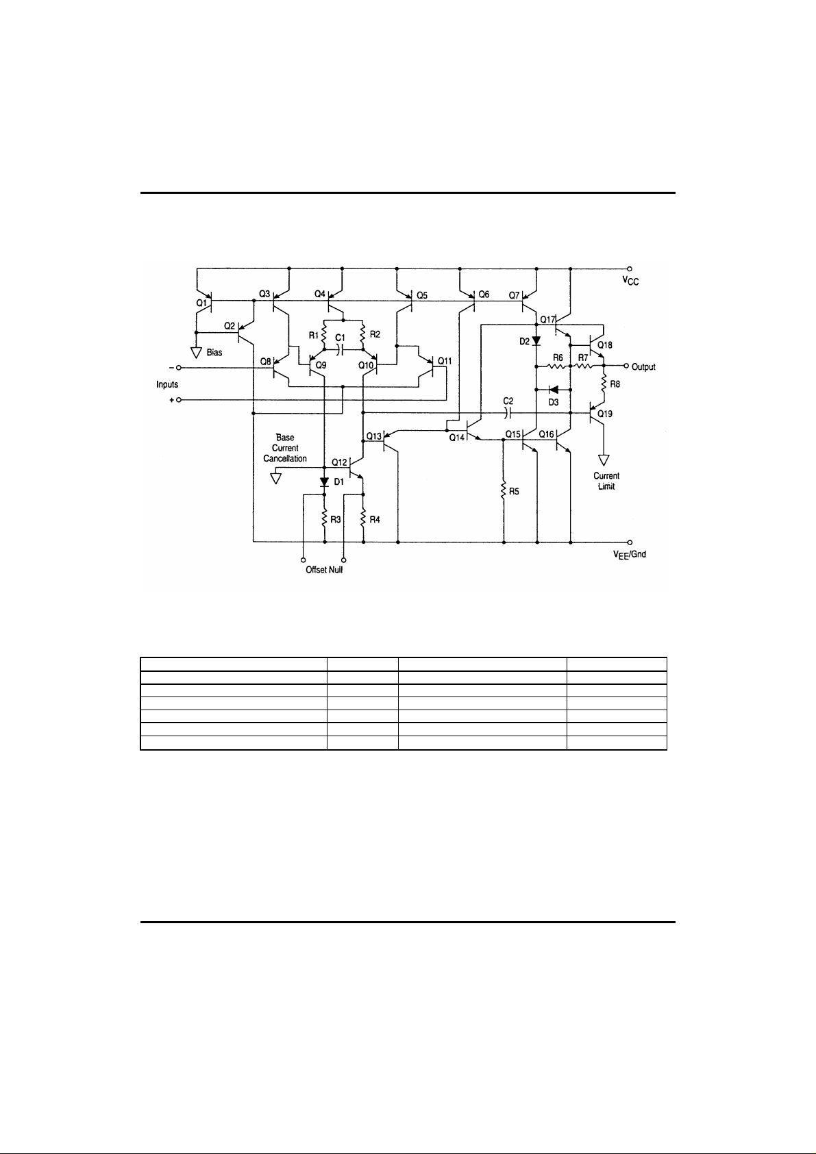
TEST CIRCUIT
ABSOLUTE MAXIMUM RATINGS(Ta=25°C )
Supply Voltage (from VEE to VCC) Vs +44 V
Differential Input Voltage VIDR Note 1 V
Input Voltage VIR Note 1 V
Output Short Circuit Duration (Note 2) tSC Indefinite sec
Operating Junction Temperature Tj +150
Storage Temperature Range Tstg -60 to 150
Notes: 1.Either or both input voltages should not exceed the magnitude of VCC or VEE.
2.Power dissipation must be considered to ensure maximum junction temperature (Tj) is not exceeded.
PARAMETER SYMBOL VALUE UNIT
°C
°C
UTC UNISONIC TECHNOLOGIES CO., LTD. 2
QW-R105-007,A
Page 3

UTC MC34072 LINEAR INTEGRATED CIRCUIT
ELECTRICAL CHARACTERISTICS(VCC=+15V, VEE=-15V, RL=connected to ground, unless otherwise
noted. )
Input Offset Voltage
(RS=100Ω,VCM=0V,Vo=0V)
Average Temperature Coefficient
of Input Offset Voltage
Input Bias Current
(VCM=0V,Vo=0V)
Input Offset Current
(VCM=0V,Vo=0V)
Input Common Mode Voltage VICR
Large Singal Voltage Gain
(Vo=+-10V,RL=2.0kΩ)
Output Voltage Swing
(VID=+-1.0V)
Output Voltage Swing
(VID=+-1.0V) VOL
Output Short Circuit current ISC
Common Mode Rejection CMR
Power Supply Rejection
(RS=100Ω)
Power Supply Current (Per
Amplifier, No Load)
PARAMETER SYMBOL TEST CONDITIONS MIN TYP MAX UNIT
VIO VCC=+15V,VEE=-15V,
TA=+25°C
VCC=+5V,VEE=0V,TA=+25°C
VCC=+15V,VEE=-15V,
∆VIO/∆T RS=10Ω,VCM=0V,VO=0V,
AVOL
VOH
PSR VCC/VEE=+16.5V/-16.5V TO
TA=0°C to 70°C
TA=0°C to 70°C
IIB
TA=+25°C
TA=0°C to 70°C
IIO
TA=+25°C
TA=0°C to 70°C
TA=+25°C
TA= TA=0°C to 70°C
TA=+25°C
TA=0°C to 70°C
VCC=+5.0V,VEE=0V,RL=2.0kΩ,
TA=+25°C
VCC=+15.0V,VEE=-15V,
RL=10kΩ,TA=+25°C
VCC=+15.0V,VEE=-15V,
RL=2.0kΩ, TA=0°C to 70°C
VCC=+5.0V,VEE=0V,RL=2.0kΩ,
TA=+25°C
VCC=+15.0V,VEE=-15V,
RL=10kΩ,TA=+25°C
VCC=+15.0V,VEE=-15V,
RL=2.0kΩ, TA=0°C to 70°C
VID=1.0V,VO=0V, TA=25°C
Source
Sink
RS<=10kΩ,VCM=VICR,TA=25°C
+13.5/-13.5V,TA=25°C
ID VCC=+5.0V,VEE=0V,VO=+2.5V,
TA=+25°C
VCC=+15.0V,VEE=-15V,
VO=0V,TA=+25°C
VCC=+15.0V,VEE=-15V,
VO=0V, TA=0°C to 70°C
13.6 14 V
13.4 V
0.5 3.0 mV
0.5 3.0 mV
5.0 mV
10
µV/°C
100 500 nA
700 nA
6.0 50 nA
VEE to (VCC –1.8) V
VEE to (VCC –2.2) V
50 100 V/mV
25 V/mV
3.7 4.0 V
-14.7 -14.3 V
10
20
80 97 dB
80 97 dB
300 nA
0.1 0.3 V
-13.5 V
30
30
1.6 2.0 mA
1.9 2.5 mA
mA
2.8 mA
UTC UNISONIC TECHNOLOGIES CO., LTD. 3
QW-R105-007,A
 Loading...