

Page 1
UTC MC3361BP LINEAR INTEGRATED CIRCUIT
LOW VOLTAGE/POWER NARROW
BAND FM IF
DESCRIPTION
The UTC MC3361BP is designed for use in FM dual
conversion communication. It contains a complete narrow
band FM demodulation system operable to less than 2.5V
supply voltage. This low-power narrow-band FM IF system
provides the second converter, second IF, demodulator. Filter
Amp and squelch circuitry for communications and scanning
receivers.
FEATURES
*Low power consumption (4.0mA typ. at Vcc=4.0V)
*Excellent input sensitivity
(-3dB limiting, 2.0µVrms typ.)
*Minimum number of external components required.
*Operating Voltage:2.5~7.0V
APPLICATIONS
*Cordless phone (for home use)
*FM dual conversion communications equipment
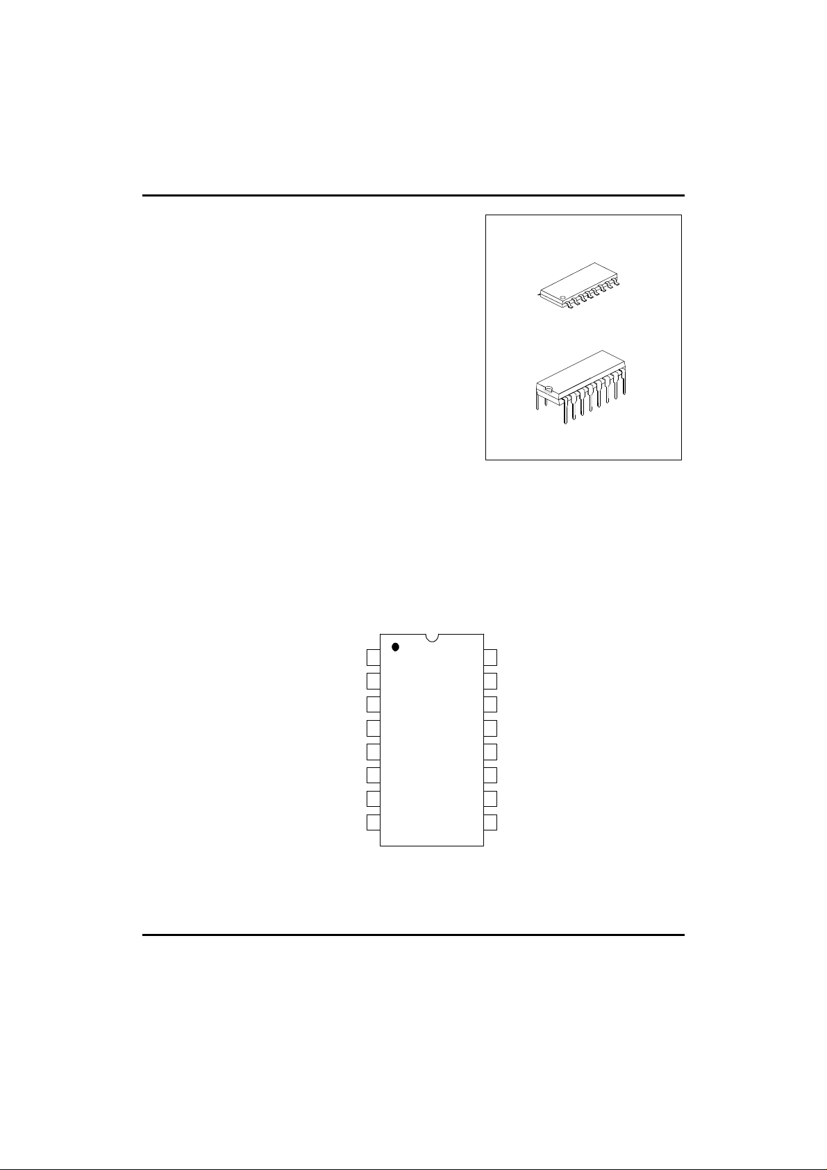
SOP-16
DIP-16
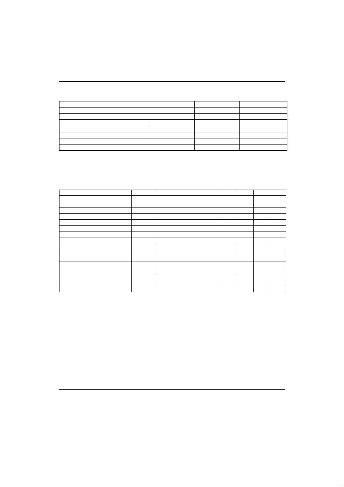
PIN CONFIGURATION
OSC
OSC
MIXER
OUTPUT
Vcc
LIMITER
INPUT
DECOUPLING
DECOUPLING
INPUT
1
2
3
4
5
6
7
8 9
16
15
14
13
CONTROL
SQUELCH
12
11
10
RF
INPUT
GND
MUTE
SCAN
INPUT
FILTER
OUTPUT
FILTER
INPUT
AUDIO
OUTPUT
UTC UNISONIC TECHNOLOGIES CO., LTD. 1
QW-R108-010,A
Page 2
UTC MC3361BP LINEAR INTEGRATED CIRCUIT
ABSOLUTE MAXIMUM RATINGS(TA=25°C)
PARAMETER SYMBOL VALUE UNIT
Max. Supply Voltage Vcc(max) 10 V
Supply Voltage Range Vcc 2.5 to 7.0 V
Detector Input voltage VI(DET) 1.0 Vp-p
RF Input Voltage (Vcc>=4.0V) VI(RF) 1.0 Vrms
Mute Function VMUTE -0.5 ~ + 5.0 Vpeak
Operating Temperature TOPR -20 to +70 °C
Storage Temperature TSTG -65 to +150 °C
Note: Absolute maximum ratings are those values beyond which permanent damage to the device may occur. These
are stress ratings only and functional operation of the device at or beyond them is not implied. Long exposure to these
conditions may affect device reliability.
ELECTRICAL CHARACTERISTICS
(Vcc=4.0V, fo=10.7MHz,∆f=+-3KHz,Ta=25°C, unless otherwise specified)
PARAMETER SYMBOL TEST CONDITIONS MIN TYP MAX UNIT
Operating Current Icc Squelch off (V12=2V)
Squelch on (V12=GND)
Input Limiting voltage VI(LIM) -3.0dB limiting 2.0 µV
Detector Output voltage VO(DET) 2.0 Vdc
Detector Output Impedance ZO(DET) 400 Ω
Audio Output Voltage VO Vin=10mV 100 160 mVrms
Filter Gain GV f=10KHz,Vin=5mV 40 48 dB
Filter Output DC Voltage VO(DC) 1.5 Vdc
Trigger Hysteresis of filter VTH 50 mV
Mute Switch-on Resistance RON(MUTE) Mute “Low” 10 Ω
Mute Switch-off Resistance ROFF(MUTE) Mute “High” 10 MΩ
Scan Control “Low” Output VL(SCAN) Mute off (V12=2V) 0.5 Vdc
Scan Control “High” Output VH(SCAN) Mute on (V12=GND) 3.0 Vdc
Mixer Conversion Gain GV(MIXER) 24 dB
Mixer Input Resistance RI(MIXER) 3.3 KΩ
Mixer Input Capacitance CI(MIXER) 2.2 pF
4.0
6.0
mA
UTC UNISONIC TECHNOLOGIES CO., LTD. 2
QW-R108-010,A
Page 3
UTC MC3361BP LINEAR INTEGRATED CIRCUIT
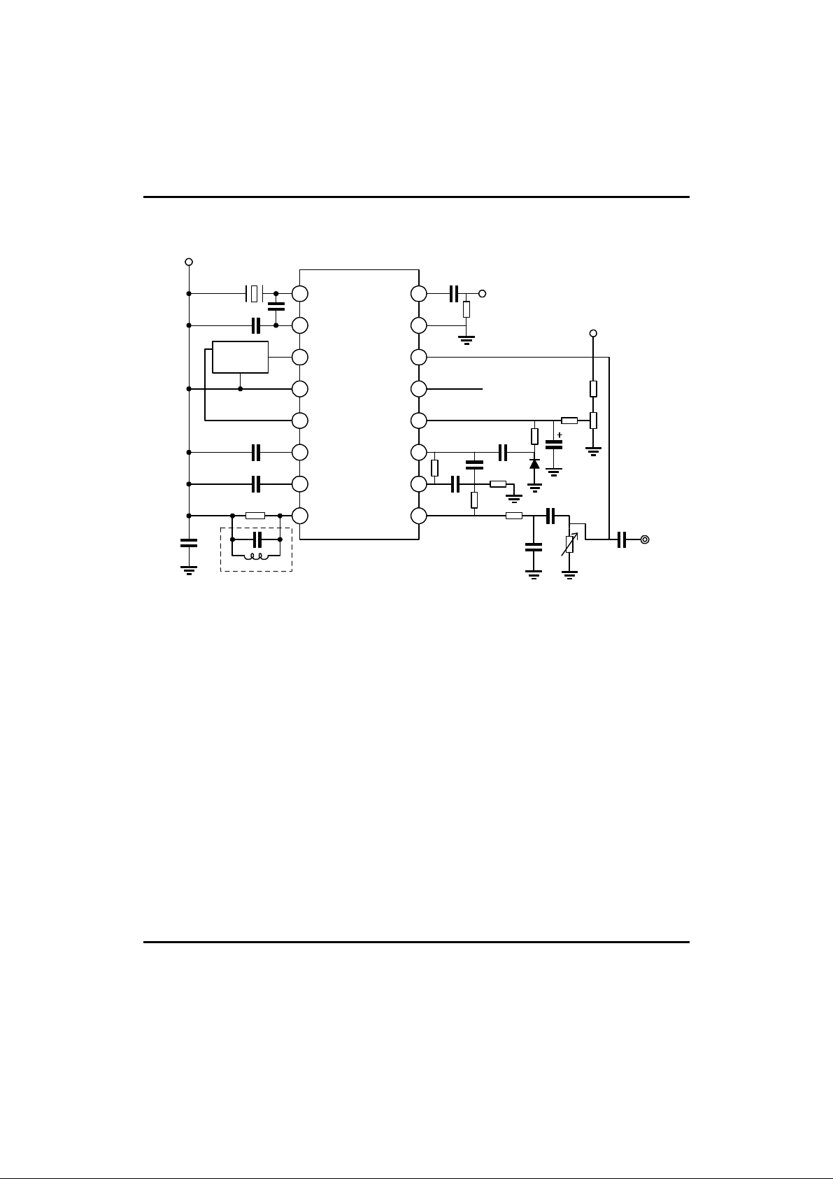
APPLICATION CIRCUIT
Vcc
10.245MHz
220p
68p
1
2
16
15
0.01
µ
RF INPUT
51K
Vcc
455KHz
FILTER
MURATA
CFU 455D
0.1
0.1
20K
0.1
µ
QUAD COIL
TOKO TYPE
RMC-2A6597HM
In the above typical application, the audio signal is recovered using a conventional quadrature FM detector. The
absence of an input signal is indicated by the presence of noise above the desired audio frequencies. This “noise
band: is monitored by an active filter and a detector. A squelch trigger circuit indicates the presence of noise (or a
tone) by an output which can be used to control scanning. At the same time, an internal switch is operated which can
be used to mute the audio.
3
4
MC3361BP
5
µ
6
µ
7
8
14
13
12
11
10
120K
0.01µF
10K
51K
50K
68K
3.3µF
SENSITIVITY
AUDIO
VOLUME
0.01µF
SQUELCH
AUDIO
OUT
SCAN
CONTROL
0.1µF
102
470K
0.1µF
9
1N4148
750
Ω
510
8.2K
0.01µF
UTC UNISONIC TECHNOLOGIES CO., LTD. 3
QW-R108-010,A
 Loading...