

Page 1
UTC LMV358 LINEAR INTEGRATED CIRCUIT
GENERAL PURPOSE, LOW
VOLTAGE, RAIL-TO-RAIL OUTPUT
OPERATIONAL AMPLIFIERS
DESCRIPTION
The UTC LMV358 are low voltage (2.7-5.5V) versions of the
dual and quad commodity op amps, LM358, which currently
operate at 5-30V. The LMV358 are the most cost effective
solutions for the applications where low voltage operation,
space saving and low price are needed. They offer
specifications that meet or exceed the familiar LM358. The
LMV358 have rail-to-rail output swing capability and the input
common-mode voltage range includes ground. They alll
exhibit excellent speed-power ratio, achieving 1 MHz of
bandwidth and 1 V/µs of slew rate with low supply current.
The chips are built with National’ s advanced submicron
silicon-gate BiCMOS process. The LMV358 have bipolar input
and output stages for improved noise performance and higher
output current drive.
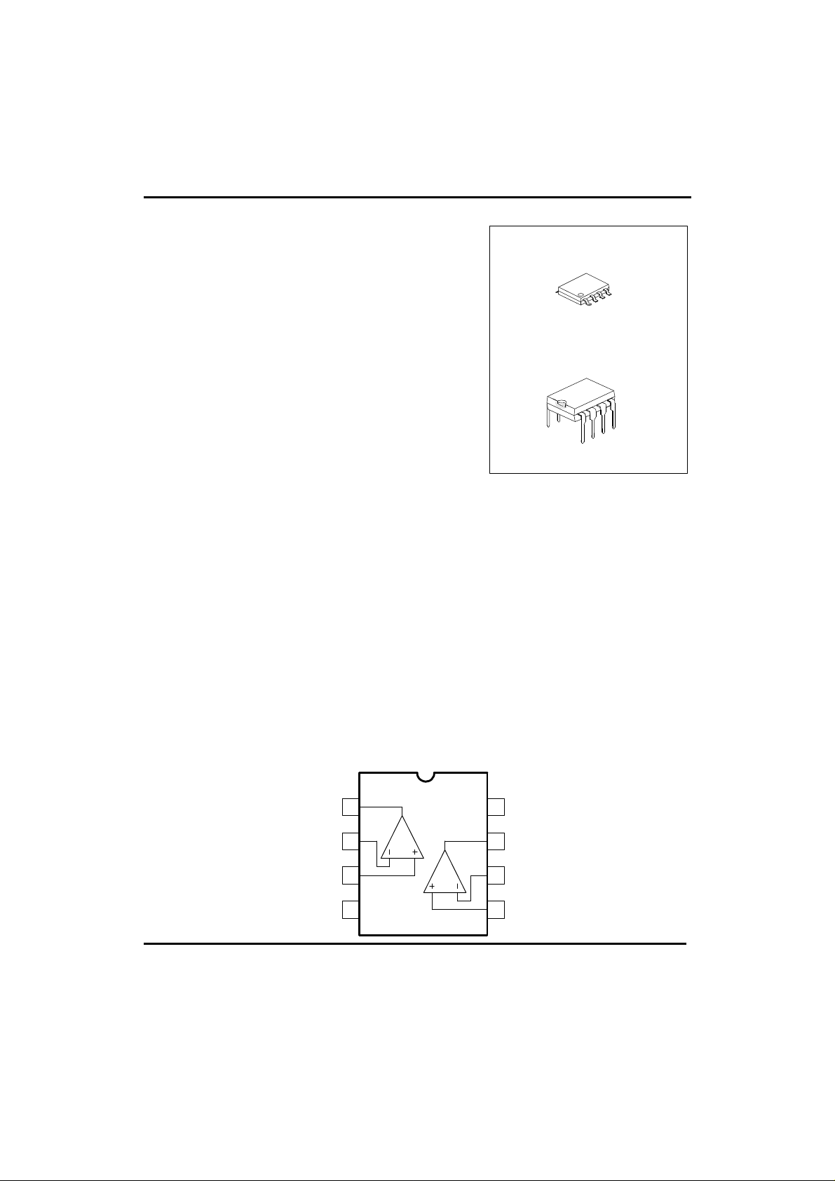
SOP-8
DIP-8
FEATURES
(For V1 =5V and V=0V. Typical Unless Otherwise Noted)
*Guaranteed 2.7V and 5V Performance
*No Crossover Distortion
*Space Saving Package
*Industrial Temp. Range
*Gain-Bandwidth Product
*Low Supply Current: 210µA
*Rail-to-Rail Output Swing
@10kΩ Load V1-10mV
V +65mV
*VCM -0.2V to V1 –0.8V
PIN CONFIGURATIONS
1
IN A-
2
3
V-
4
APPLICATIONS
*Active Filters
*General Purpose Low Voltage Applications
*General Purpose Portable Devices
8
V+OUT A
A
B
OUT B
7
6
IN B-IN A+
IN B+
5
UTC UNISONIC TECHNOLOGIES CO.,LTD.
QW-R105-010,A
1
Page 2
UTC LMV358 LINEAR INTEGRATED CIRCUIT
ABSOLUTE MAXIMUM RATINGS
PARAMETER VALUE UNIT
ESD Tolerance(Note 2)
Machine Model 100 V
Human Body Model 2000 V
Differential Input Voltage +-Supply Voltage
Supply Voltage (V1-V) 5.5 V
Output Short Circuit to V
Output Short Circuit to V (Note 4)
Mounting Temp.
Lead Temp. (Soldering 10 sec) 260 °C
Infrared (15 sec) 215 °C
Storage Temp. Range -65 to 150 °C
Junction Temp. (Tj, max) (Note 5) 150 °C
OPERATING RATINGS (NOTE 1)
Supply Voltage 2.7 to 5.5 V
Temperature Range -40<=Tj<=85 °C
Thermal Resistance (θJA) (Note 10) 235 °C/W
2.7V DC ELECTRICAL CHARACTERISTICS
Unless otherwise specified, all limits guaranteed for Tj=25°C, V1=2.7V, V=0V, VCM=1.0V, Vo=V1/2 and RL=1MΩ
PARAMETER SYMBOL CONDITIONS TYP
Input Offset Voltage Vos 1.7 7 mV
Input Offset Voltage Average Drift TCVos 5 µV/°C
Input Bias Current Is 11 250 nA
Input Offset Current Ios 5 50 nA
Common Mode Rejection Ratio CMRR 0V<=VCM<=1.7V 63 50 dB
Power Supply Rejection Ratio PSRR 2.7V<=V1 <=5V
Input Common-Mode Voltage Range VCM For CMRR>=50dB -0.2 0 V
Output Swing Vo RL=10kΩ to 1.35V V1-10 V1-100 mV
Supply Current Is Both amplifiers 140 340 µA
1
PARAMETER VALUE UNIT
Vo=1V
(Note 3)
LIMIT
(note6)
60 50 dB
1.9 1.7 V
60 180 mV
(note7)
UNIT
max
max
max
min
min
min
max
min
max
UTC UNISONIC TECHNOLOGIES CO.,LTD.
QW-R105-010,A
2
Page 3
UTC LMV358 LINEAR INTEGRATED CIRCUIT
PARAMETER SYMBOL CONDITIONS TYP
(note6)
2.7V AC ELECTRICAL CHARACTERISTICS
Unless otherwise specified, all limits guaranteed for Tj=25°C, V1=2.7V, V=0V, VCM=1.0V, Vo=V1/2 and RL>1MΩ
PARAMETER SYMBOL CONDITIONS TYP
(note6)
Gain-Bandwidth Product GBWP CL=200pF 1 MHz
Phase Margin Φ(T) 60 Deg
Gain Margin G(r) 10 dB
Input-Referred Voltage Noise θr1 F=1kHz 46 nV
Input-referred Current Noise Ir1 F=1kHz 0.17 pA
5V DC ELECTRICAL CHARACTERISTICS
Unless otherwise specified, all limits guaranteed for Tj=25°C, V1=5V, V=0V, VCM=2.0V, Vo=V1/2 and RL>1MΩ.
Boldface limits apply at the temperature extremes.
PARAMETER SYMBOL CONDITIONS TYP LIMIT UNIT
Input Offset Voltage Vos 1.7 7
Input Offset Voltage Average Drift TCVos 5 µV/°C
Input Bias Current IB 15 250
Input Offset Current Ios 5 50
Common Mode Rejection Ratio CMRR 0V<=VCM<=4V 65 50 dB
Power Supply Rejection Ratio PSRR 2.7V<=V1<=5V
Vo=1V VCM=1V
Input Common-Mode Voltage Range VCM For CMRR>=50dB -0.2 0 V
Large Signal Voltage Gain(Note 8) Av RL=2kΩ 100 15
Output Swing Vo RL=2kΩ to 2.5V V1-40 V1-300
Vo RL=10kΩ to 2.5V V1-10 V1-100
Output Short Circuit Current Io Sourcing,Vo=0V 60 5 mA
60 50 dB
4.2 4 V
120 300
65 180
LIMIT
(note7)
LIMIT
(note7)
9
500
150
10
V+-400
400
V+-200
280
UNIT
max
UNIT
√ Hz
√ Hz
mV
max
nA
max
nA
max
min
min
min
max
V/mV
min
mV
min
mV
max
mV
min
mV
max
min
UTC UNISONIC TECHNOLOGIES CO.,LTD.
QW-R105-010,A
3
Page 4

UTC LMV358 LINEAR INTEGRATED CIRCUIT
PARAMETER SYMBOL CONDITIONS TYP LIMIT UNIT
Sinking,Vo=5V 160 10 mA
min
Supply Current Is Both amplifiers 210 440
615
2.5V AC ELECTRICAL CHARACTERISTICS
Unless otherwise specified, all limits guaranteed for Tj=25°C, V1=2.7V, V=0V, VCM=2.0V, Vo=V1/2 and RL>1MΩ
PARAMETER SYMBOL CONDITIONS TYP LIMIT UNIT
Slew Rate SR (Note 9) 1 V/µs
Gain-Bandwidth Product GBWP CL=200pF 1 MHz
Phase Margin Φ(T) 60 Deg
Gain Margin G(r) 10 dB
Input-Referred Voltage Noise θr1 f=1kHz 39 nV
Input-referred Current Noise Ir1 f=1kHz 0.21 pA
Note1: Absolute Maximum Ratings indicate limits beyond which damage to the device may occur. Operating
Ratings indicate conditions for which the device is intended to be functional, but specific performances is not
guaranteed. For guaranteed specifications and the test conditions, see the Electrical Characteristics.
Note2: Human body model 1.5kΩ in series with 100pF. Machine model, 0Ω in series with 200pF.
Note3: Shorting output to V1 will adversely after reliability.
Note4: Shorting output to V+ will adversely affect reliability.
Note5: The maximum power dissipation is a function of Tj(max) θJA and TA. The maximum allowable power
dissipation at any ambient temperature is PD=(Tj(max)-TA)/θJA. All numbers apply for packages soldered
directly into a PC board.
Note6: Typical values represent the most likely parametric norm.
Note7: All limits are guaranteed by testing or statistical analysis.
Note8: RL is connected to V. The output voltages is 0.5V<=Vo<=4.5V.
Note9: Connected as voltage follower with 3V step input. Number specified is thes lower of the positive and
negative slew rates.
Note10: all numbers are typical, and apply for packages soldered directly note a PC board is still air.
µA
max
√ Hz
√ Hz
UTC UNISONIC TECHNOLOGIES CO.,LTD.
QW-R105-010,A
4
Page 5

UTC LMV358 LINEAR INTEGRATED CIRCUIT
TYPICAL PERFORMANCE CHARACTERISTICS
(Unless otherwise specified,VE=+5V,single supply. TA=25°C)
UTC UNISONIC TECHNOLOGIES CO.,LTD.
QW-R105-010,A
5
Page 6

UTC LMV358 LINEAR INTEGRATED CIRCUIT
UTC UNISONIC TECHNOLOGIES CO.,LTD.
QW-R105-010,A
6
Page 7

UTC LMV358 LINEAR INTEGRATED CIRCUIT
UTC UNISONIC TECHNOLOGIES CO.,LTD.
QW-R105-010,A
7
Page 8

UTC LMV358 LINEAR INTEGRATED CIRCUIT
UTC UNISONIC TECHNOLOGIES CO.,LTD.
QW-R105-010,A
8
Page 9

UTC LMV358 LINEAR INTEGRATED CIRCUIT
UTC UNISONIC TECHNOLOGIES CO.,LTD.
QW-R105-010,A
9
 Loading...