

Page 1
UTC BT169 SCR
DESCRIPTION
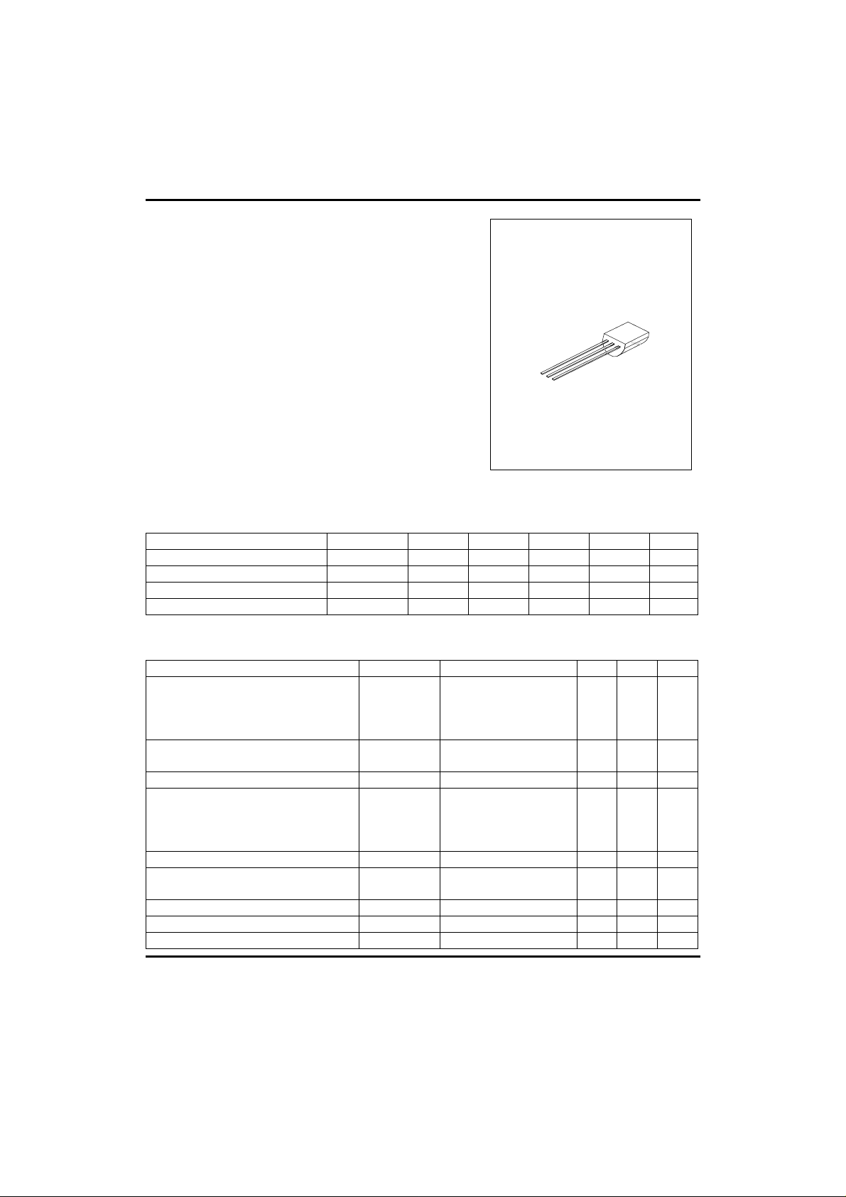
The UTC BT169 is glass passivated, sensitive gate
thyristors in a plastic envelope, intended for use in
general purpose switching and phase control
applications. These devices are intended to be
interfaced directly to microcontrollers, logic integrated
circuits and other low power gate trigger circuits.
1:CATHODE 2:GATE 3:ANODE
QUICK REFERENCE DATA
PARAMETER SYMBOL MAX(B) MAX(D) MAX(E) MAX(G) UNIT
Repetitive peak off-state voltages VDRM, VRRM 200 400 500 600 V
Average on-state current IT(AV) 0.5 0.5 0.5 0.5 A
RMS on-state current IT(RMS) 0.8 0.8 0.8 0.8 A
Non-repetitive peak on-state current ITSM 8 8 8 8 A
1
TO-92
ABSOLUTE MAXIMUM RATINGS
PARAMETER SYMBOL CONDITIONS MIN MAX UNIT
Repetitive peak off-state voltages : VDRM,VRRM B:200
D:400
E:500
G:600
Average on-state current IT(AV) Half sine wave;
Tlead<=83°C
RMS on-state current IT(RMS) All conduction angles 0.8 A
Non-repetitive peak on-state current ITSM t=10ms
t=8.3ms
half sine wave;
Tj=25°C prior to surge
I2t for fusing I2t t=10ms 0.32 A2S
Repetitive rate of rise of on-state current
after triggering
Peak gate current IGM 1 A
Peak gate voltage VGM 5 V
Peak reverse gate voltage VRGM 5 V
DIT/dt ITM=2A;IG=10mA;
dIG/dt=100mA/µs
0.5 A
V
8
A
9
50 A/µs
UTC UNISONIC TECHNOLOGIES CO., LTD.
1
Page 2
UTC BT169 SCR
PARAMETER SYMBOL CONDITIONS MIN MAX UNIT
Peak gate power PGM 2 W
Average gate power PG(AV) Over any 20 ms period 0.1 W
Storage temperature Tstg -40 150 °C
Operating junction temperature Tj 125 °C
THERMAL RESISTANCES
PARAMETER SYMBOL CONDITIONS MIN TYP MAX UNIT
Thermal resistance junction to lead Rth j-lead 60 K/W
Thermal resistance junction to
ambient
ELECTRICAL CHARACTERISTICS (Tj=25°C unless otherwise stated)
PARAMETER SYMBOL CONDITIONS MIN TYP MAX UNIT
STATIC
Gate trigger current IGT VD=12V;IT=10mA;gate
Latching current IL VD=12V;IGT=0.5mA;
Holding current IH VD=12V;IGT=0.5mA;
On-state voltage VT IT=1A 1.2 1.35 V
Gate trigger voltage VGT VD=12V;IT=10mA;
Off-state leakage current ID,IR VD=VDRM(max) ;VR=VRRM(m
DYNAMIC
Ciritical rate of rise of off-state
voltage
Gate controlled turn-on time t
Circuit commutated turn-off time tq VD=67% VDRM(max) ;
Rth j-a pcb mounted;
lead length=4mm
open circuit
RGK=1kΩ
RGK=1kΩ
gate open circuit
VD=VDRM(max) ;IT=10mA ;
Tj=125°C; gate open circuit
ax) ;Tj=125°C;RGK=1kΩ
dVD/dt VDM=67% VDRM(max);
Tj=125°C; exponential
waveform;RGK=1kΩ
gt
ITM=2A;VD=VDRM(max);
IG=10mA;dIG/dt=0.1A/µs
Tj=125°C;ITM=1.6A;VR=35V
;dITM/dt=30A/µs;
VD/dt=2V/µs;RGK=1kΩ
150 K/W
50 200 µA
2 6 mA
2 5 mA
0.5
0.2
0.3
0.05 0.1 mA
25 V/µs
2 µs
100 µs
0.8 V
UTC UNISONIC TECHNOLOGIES CO., LTD.
2
Page 3

UTC BT169 SCR
1.9
Tc(max) / C
a=1.57
tot
, versus average
T(RMS)
/ I
77
83
89
95
101
107
113
119
125
T(AV)
P
tot
/ W
0.8
conduction
form
angle
degrees
30
60
90
120
180
factor
a
4
2.2
2.8
2.2
2.8
1.9
1.57
4
0.7
0.6
0.5
0.4
0.3
0.2
0.1
0
0 0.1 0.2 0.3 0.4 0.5 0.6 0.7
FIG.1 Maximum on-state dissipation, P
on-state current, I
IF(AV) / A
T(AV)
, where a=form factor=I
ITSM / A
1000
100
I
TSM
I
T
10
1
FIG.2 Maximum permissible non-repetitive peak on-state current
I
TSM
1.0
0.8
T
time
Tj initial=25¢XC max
10µs
100µs 1ms 10ms
T / s
,versus pulse width tp,for sinusoidal currents, tp<=10ms.
IT(RMS) / A
83¢XC
0.6
0.4
0.2
0
-50 0
FIG.3 Maximum permissible rms current I
50 100 150
Tlead / C
lead temperature, Tlead
T(RMS)
, versus
ITSM / A
10
I
TSM
I
T
8
T
6
time
Tj initial=25¢XC max
4
2
0
1
10 100 1000
Number of half cycles at 50Hz
FIG.4 Maximnum permissible non-repetitive peak on-state current
I
TSM
, versus number of cycles, for sinusoidal currents, f = 50Hz.
IT(RMS) / A
2.0
1.5
1.0
0.5
0
0.01
0.1 1.0 10
surge duration / s
FIG.5 Maximum permissible repetitive rms on-state current I
versus surge duration, for sinusoidal currents, f= 50Hz; Tlead<=83¢XC
VGT(Tj)
VGT(25¢XC)
1.6
T(RMS)
1.4
1.2
1.0
0.8
0.6
0.4
-50 0
FIG.6 Normalised gate trigger voltage VGT(Tj)/V
versus junction temperature Tj
50 100 150
Tj / C
GT(
25¢XC),
,
UTC UNISONIC TECHNOLOGIES CO., LTD.
3
Page 4

UTC BT169 SCR
FIG.11 Transient thermal impedance Zth j-lead, versus pulse width tp.
IGT(Tj)
VGT(25¢XC)
3.0
2.5
2.0
1.5
1.0
0.5
0
-50 0
FIG.7 Normalised gate trigger current IGT(Tj)/IGT(25¢XC),
3.0
2.5
2.0
1.5
1.0
0.5
FIG.8 Normalised latching current IL(Tj)/IL(25¢XC),versus
versus junction temperature Tj
IL(Tj)
IL(25¢XC)
0
-50 0
junction temperature Tj, RGK= 1K
50 100 150
Tj / C
50 100 150
Tj / C
Ω
IT / A
5
Tj=125¢XC - - Tj= 25¢XC
4
Vo=1.067V
Rs=0.187
3
2
1
0
FIG.10 Typical and maximum on-state characteristic.
100
10
1
0.1
0.01
10us
Ω
0 0.5
Zth j-lead (K/W)
1ms
0.1ms 10ms 1s
typ max
1.0 1.5 2.0
VT / V
PD
tp
0.1s
tp / s
t
10s
IH(Tj)
IH(25¢XC)
3.0
2.5
2.0
1.5
1.0
0.5
0
-50 0
FIG.9 Normalised holding current IH(Tj)/IH(25¢XC),versus
junction temperature Tj, RGK=1K
50 100 150
Tj / C
Ω
dVD/dt(V/us)
1000
100
10
1
0 0
FIG.12 Typical, critical rate of rise of off-state voltage,
dVD/dt versus junction temperature Tj.
Tj / C
RGK=1K
Ω
50 150
UTC UNISONIC TECHNOLOGIES CO., LTD.
4
 Loading...