

Page 1
UTC 51494 LINEAR INTEGRATED CIRCUIT
DESCRIPTION
The UTC 51494 is a monolithic bipolar integrate circuit that
provides both 494 function and built in power good signal
circuit for easy using 51494 can be easily implemented by just
adding a capacitor.
FEATURES
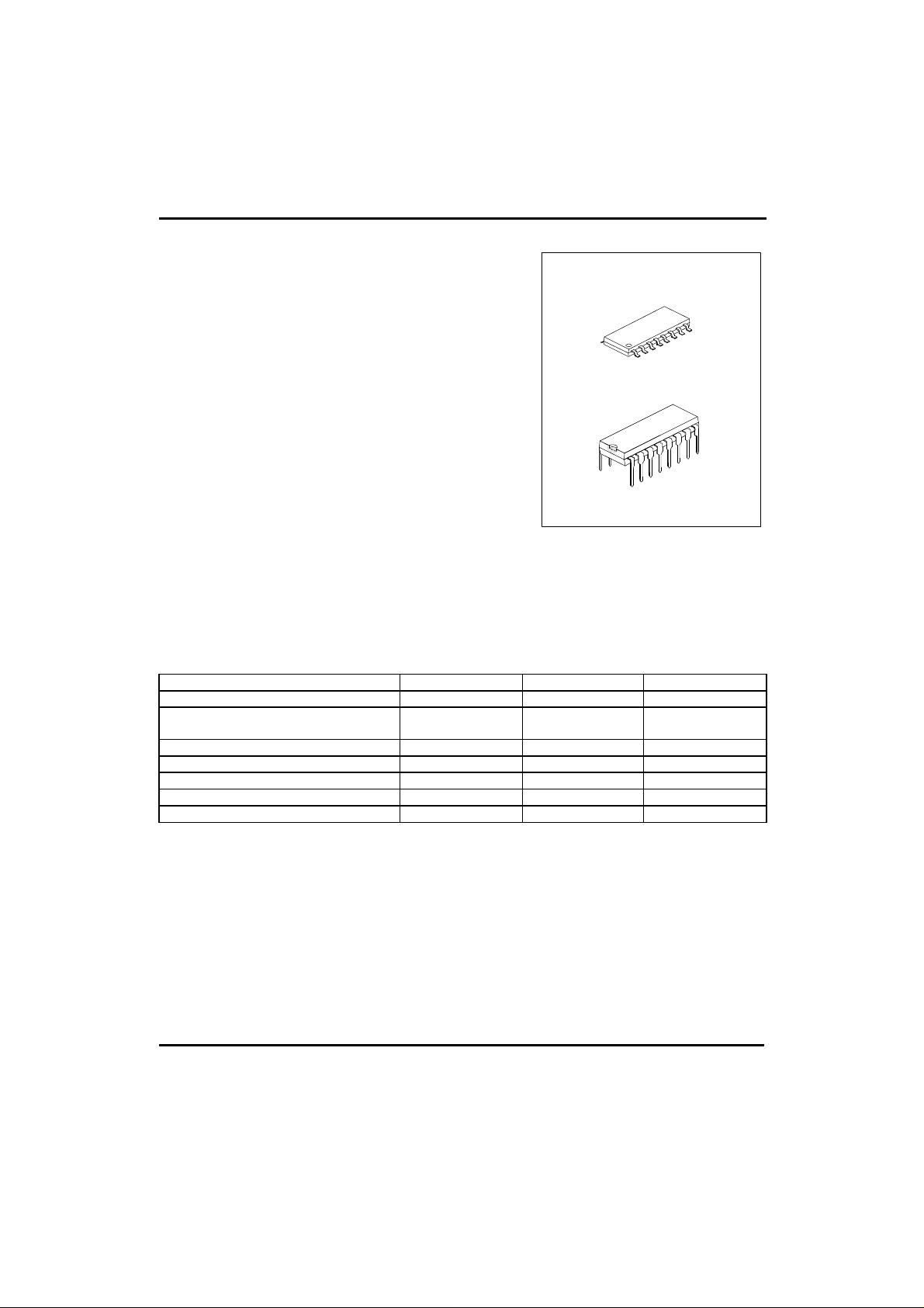
*Fully integrated with compact 16-pin dip
*All necessary functions included for most popular half
bridge circuit.
*Built-in power good delay and power fail lead function.
*Power good delay time is linearly.
*Proportional to external capacitor value.
*Reduced external components for cost down and
components for cost down and compact size.
SOP-16
DIP-16
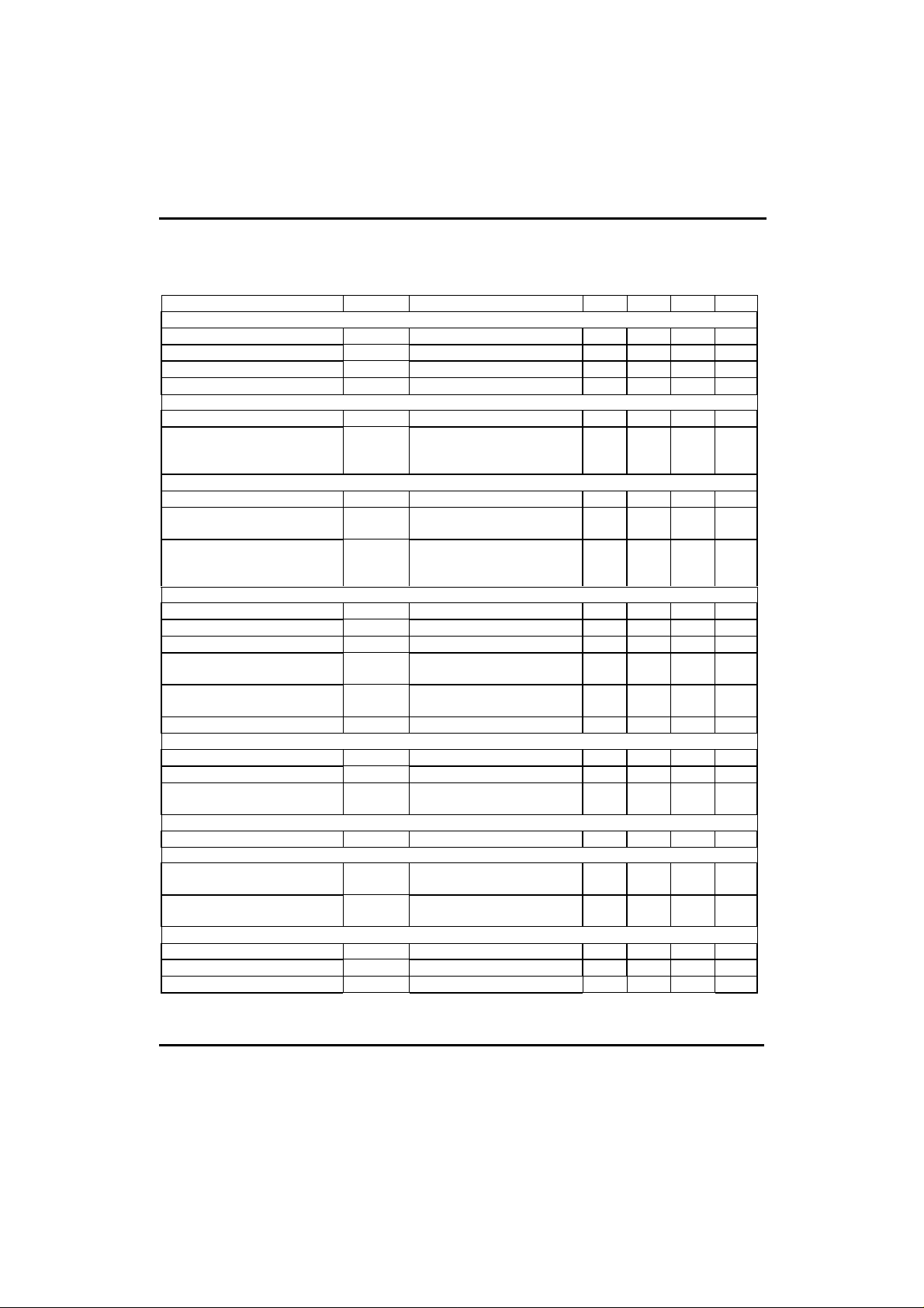
MAXIMUM RATINGS(Unless otherwise noted ,all is over operating free-air temperature Range)
CHARACTERISTIC SYMBOL RATING UNIT
Supply Voltage Vcc 42 V
Voltage from any pin to ground (except pin8 &
pin11)
Collector Output Voltage Vc1, Vc2 42 V
Peak Collector Output Ic1, Ic2 250 mA
Power dissipation PD 1500 mW
Operating Temperature Range Topr 0 to +70 °C
Storage Temperature Range Tsag -65 to +150 °C
Vin Vcc+0.3 V
UTC UNISONIC TECHNOLOGIES CO. LTD
QW-R103-005,A
1
Page 2
UTC 51494 LINEAR INTEGRATED CIRCUIT
ELECTRICAL CHARACTERISTICS
(Unless otherwise specified , Ta=0~70°C ,VCC=15V,f=10kHz,)
PARAMETER SYMBOL TEST CONDITIONS MIN TYP MAX UNIT
Reference Section
Reference voltage Vref Iref =1.0mA 4.75 5 5.25 V
Line Regulation Vline 7V<Vcc<40V 2 25 mV
Load Regulation Viload 1mA<Iref<5mA 1 15 mV
Temperature Coefficient 0°C <Fa<70°C 0.01 0.03 %/°C
Oscillator section
Oscillator Frequency Fosc CT=0.01µF,RT=12kΩ 10 kHz
Oscillator Frequency Change
Over Operating Temperature
Range
Dead Time Control Section
Input Bias Current ( Pin 4 ) Iib(dt) Vcc =15V ; 0V<V4<5.25V -2 -10 µA
Maximum Duty cycle,
Each output
Input Threshold Voltage :
Zero Duty
Max Duty
Error Amplifier Section
Input offset Voltage Vics V3=2.5V 2 10 mV
Input offset Current Iics V3=2.5V 25 250 nA
Input bias Current Iib V3=2.5V 0.2 1 µA
Input Common-mode Voltage
Range
Large Signal Open-Loop Voltage
Range
Unity-Gain Band width fc 650 kHz
Output Section
Collector off-state current Ic(off) VCC=VC=40V,VE=0 2 100 µA
Emitter off-state Current Ie(off) VCC=VC=40V,VE=0 -100 µA
Output Saturation Voltage
Common-Emitter
Output Control (pin13)
Standby Power Supply Current Icc 6 10 mA
Output AC Characteristic
Raise Time
Common-Emitter
Fall Time
Common-Emitter
PWM Comparator Section
Inhibit Threshold Voltage Vthi Zero Duty cycle 4 4.5 V
Output Source Current Io+ 0.5V < V3 < 3.5V 2 mA
Output Sink Current Io- 0.5V < V3 < 3.5V -0.2 -0.6 mA
∆fosc CT=0.01µF,RT=12kΩ
Dc(max) Vcc = 15V; Pin 4 = 0V
Output Control Pin = Vref
Vth
Vicr 7V <Vcc< 40V -0.3 Vcc V
Gvo 0.5V < V3 < 3.5V 60 74 dB
Vce(sat) VE=15V,Lc=200mA 1.1 1.3 V
Tr 100 200 ns
Tr 25 100 ns
43 45 %
0
2 %
3 3. 3 V
UTC UNISONIC TECHNOLOGIES CO. LTD
QW-R103-005,A
2
Page 3

UTC 51494 LINEAR INTEGRATED CIRCUIT
PARAMETER SYMBOL TEST CONDITIONS MIN TYP MAX UNIT
Power Good Section
Power Good Delay Time tpd Cd = 1µ 230 280 330 ms
Cd = 0.47µ 108 130 160
Power Fail Lead Time Tp1 4 ms
Output High Voltage Voh Vpinn = 5V, IL = 1mA 4.75 V
Output Saturation Voltage Vsat Vpinn = 5V, Isink = 4mA 0.4 V
Output Leakage Current Ioh 100 µA
PIN DESCRIPTION
PIN NAME FUNCTION
1 EA1+ Error amplifier noninverting input, same as pin 1 of 494
2 EA1- Error amplifier inverting input, same as pin 2 of 494
3 EA0 Error amplifier output and feedback, same as pin 3 of 494
4 DT Dead time control input, same as pin 4 of 494
5 CT Connect capacitor to oscillator circuit for operating frequency, same as pin 5 of 494
6 RT Connect resistor to oscillator circuit for operating frequency, same as pin 6 of 494
7 GND Ground terminal of IC, same as pin 7 of 494
8 C1 Collector of output transistor one, same as pin 8 of 494
9 GND Ground terminal of IC
10 Cpg Terminal for capacitor to determine power good delay time
11 C2 Collector of output transistor two, same as pin 11 of 494
12 Vcc Supply voltage, same as pin 12 of 494
13 P.G. Output for power good signal
14 Vref Reference voltage output, same as pin 14 of 494
15 EA2- Error amplifier inverting input, same as pin 15 of 494
16 EA+ Error amplifier noninverting input, same as pin 16 of 494
UTC UNISONIC TECHNOLOGIES CO. LTD
QW-R103-005,A
3
Page 4

UTC 51494 LINEAR INTEGRATED CIRCUIT
BLOCK DIAGRAM
12
Vcc
Ref Out
GND
RT
CT
Dead-Time
Control
Non-inv Input
Inv Input
Non Inv Input
Inv Input
Feed-Back
14
7
6
5
Reference
Regulator
Osc
TF.E
C1
C2
GND
8
11
9
Dead Time
COMPARATOR
+
4
1
2
16
15
-
+
-
EA1
+
EA2
+
-
PWM
COMPARATOR
P.G.
3
-
+
13
1.25V
10
Cpg
UTC UNISONIC TECHNOLOGIES CO. LTD
QW-R103-005,A
4
Page 5

UTC 51494 LINEAR INTEGRATED CIRCUIT
UCC
1.5K
0.01uF
3 14 13 12 11
4.7K
43K
2
8
51494
1
7
16
15109654
4.7K
270
2.2U
2.2K
4.7K
4148
4.7K
12K
0.001U
22K
0.68U
100K
150K
-5U
-12
+5
POWER GOOD
UTC UNISONIC TECHNOLOGIES CO. LTD
QW-R103-005,A
5
 Loading...