

Datasheet UT62L5128SC-100LLI, UT62L5128SC-100LI, UT62L5128LS-70LLI, UT62L5128LS-70LI, UT62L5128LS-55LLI Datasheet (UTRON)
...Page 1
UTRON
UT62L5128(I)
Preliminary Rev. 0.7
512K X 8 BIT LOW POWER CMOS SRAM
UTRON TECHNOLOGY INC. P80052
1F, No. 11, R&D Rd. II, Science-Based Industrial Park, Hsinchu, Taiwan, R. O. C.
TEL: 886-3-5777882 FAX: 886-3-5777919
1
FEATURES
Access time : 55/70/100 ns
CMOS Low operating power
Operating : 45/35/25mA (max.)
Standby : 20µA (typ.) L-version
3µA (typ.) LL-version
Single 2.7V~3.6V power supply
Industrial Temperature : -40℃~85℃
All inputs and outputs TTL compatible
Fully static operation
Three state outputs
Data retention voltage : 1.5V (min)
Package : 32-pin 450 mil SOP
32-pin 8mm×20mm TSOP-I
32-pin 8mm×13.4mm STSOP
36-pin 6mm×8mm TFBGA
GENERAL DESCRIPTION
The UT62L5128 is a 4,194,304-bit low power
CMOS static random access memory organized as
524,288 words by 8 bits. It is fabricated using high
performance, high reliability CMOS technology.
The UT62L5128 operates from a wide range
2.7V~3.6V power supply and all inputs and
outputs are fully TTL compatible.
The UT62L5128 supports industrial operating
temperature range, and supports low data
retention voltage for battery back-up operation
with low data retention current.
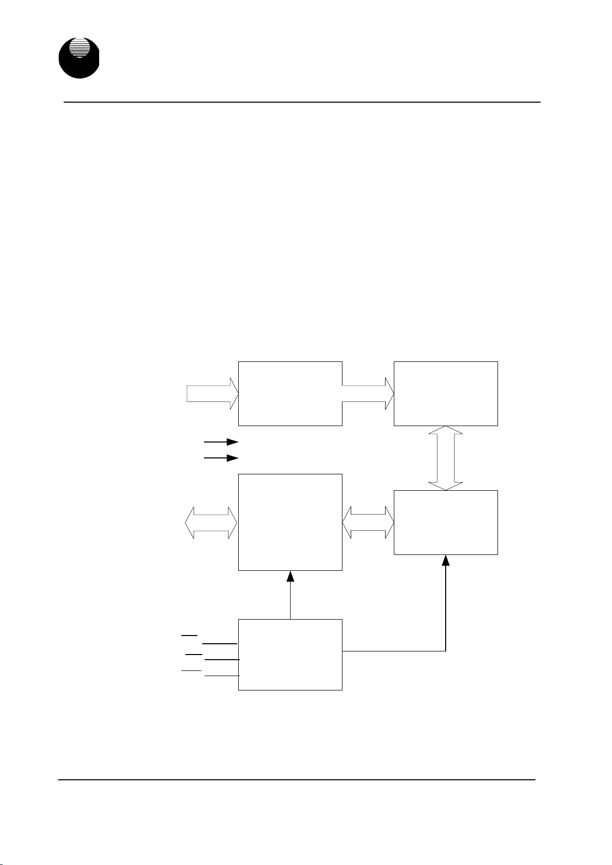
FUNCTIONAL BLOCK DIAGRAM
DECODER
I/O DATA
CIRCUIT
CONTROL
CIRCUIT
512K ×8
MEMORY
ARRAY
COLUMN I/O
OE
WE
A0-A18
Vcc
Vss
I/O1-I/O8
CE
Page 2
UTRON
UT62L5128(I)
Preliminary Rev. 0.7
512K X 8 BIT LOW POWER CMOS SRAM
UTRON TECHNOLOGY INC. P80052
1F, No. 11, R&D Rd. II, Science-Based Industrial Park, Hsinchu, Taiwan, R. O. C.
TEL: 886-3-5777882 FAX: 886-3-5777919
2
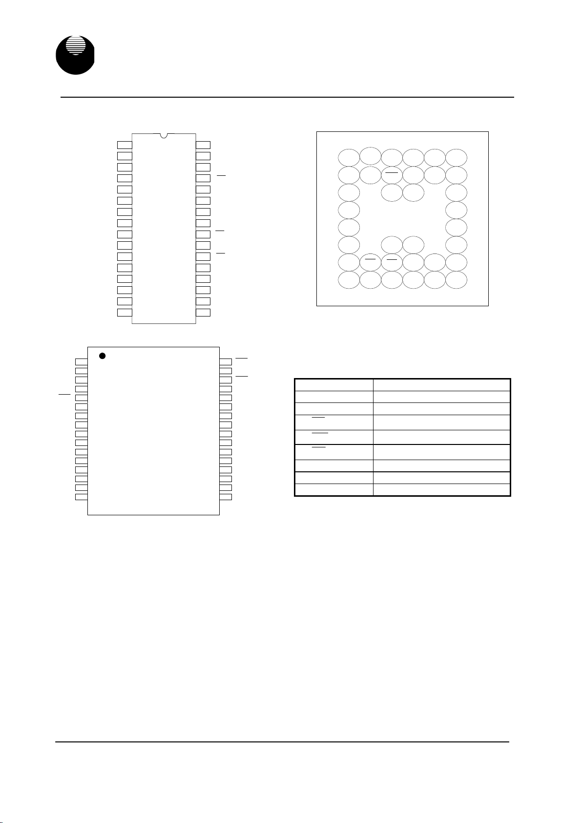
PIN CONFIGURATION
SOP
A12
A7
A6
A5
A4
A3
A2
A1
A0
I/O1
I/O2
A17
A8
A9
A11
A10
I/O8
I/O7
I/O6
I/O5
I/O4
I/O3
Vss
28
14
13
12
11
10
9
8
7
6
5
4
3
2
1
1716
15
20
19
18
22
23
24
25
26
27
21
A13
A14
A18
A16
Vcc
A15
29
30
31
32
OE
CE
WE
I/O4
A11
A9
A8
A13
I/O3
A10
A14
A12
A7
A6
A5
Vcc
I/O8
I/O7
I/O6
I/O5
Vss
I/O2
I/O1
A0
A1
A2
A4 A3
TSOP-1 / STSOP
28
14
13
12
11
10
9
8
7
6
5
4
3
2
1
17
16
15
20
19
18
22
23
24
25
26
27
21
WE
OE
CE
A17
A18
A15
32
31
30
29
A16
OE CE
WE
A12A11 A13
NC
A17
A10 A14
A15
I/O6
I/O7
I/O8
A9
Vss
A8
A16
I/O5
Vcc
Vcc
I/O4
A18
Vss
A7
A0
I/O3
I/O2
I/O1
A6A1 A3
A5NC
A4A2
123456
H
G
C
D
E
F
A
B
TFBGA
PIN DESCRIPTION
SYMBOL DESCRIPTION
A0 - A18 Address Inputs
I/O1 - I/O8 Data Inputs/Outputs
CE
Chip Enable Input
WE
Write Enable Input
OE
Output Enable Input
Vcc Power Supply
Vss Ground
NC No Connection
Page 3
UTRON
UT62L5128(I)
Preliminary Rev. 0.7
512K X 8 BIT LOW POWER CMOS SRAM
UTRON TECHNOLOGY INC. P80052
1F, No. 11, R&D Rd. II, Science-Based Industrial Park, Hsinchu, Taiwan, R. O. C.
TEL: 886-3-5777882 FAX: 886-3-5777919
3
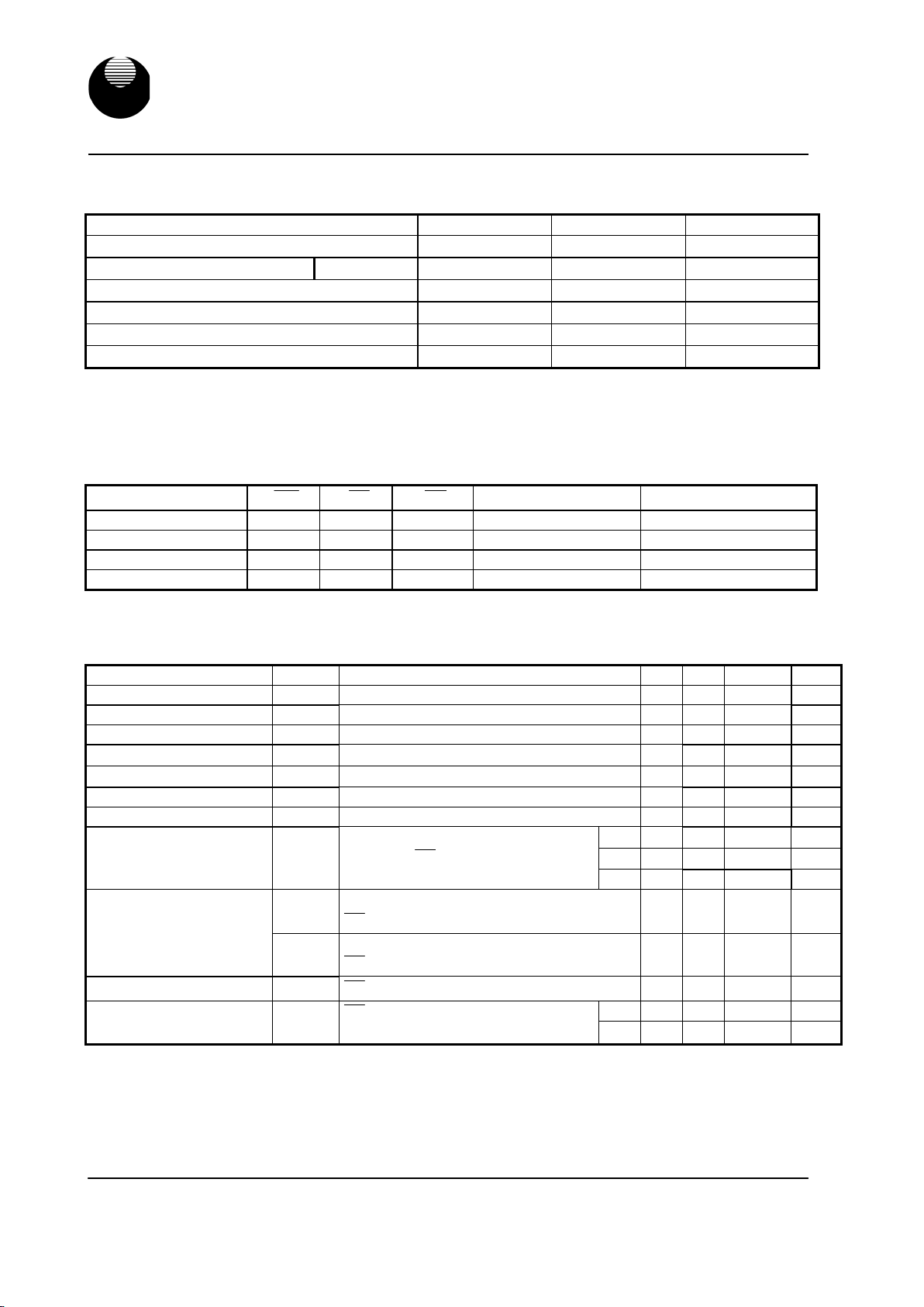
ABSOLUTE MAXIMUM RATINGS
*
PARAMETER SYMBOL RATING UNIT
Terminal Voltage with Respect to VSS V
TERM
-0.5 to 4.6 V
Operating Temperature
Industrial T
A
-40 to 85
℃
Storage Temperature T
STG
-65 to 150
℃
Power Dissipation PD 1 W
DC Output Current I
OUT
50 mA
Soldering Temperature (under 10 secs) Tsolder 260
℃
*Stresses greater than those listed under “Absolute Maximum Ratings” may cause permanent damage to the device. This is a stress
rating only and functional operation of the device or any other conditions above those indicated in the operational sections of this
specification is not implied. Exposure to the absolute maximum rating conditions for extended period may affect device reliability.
TRUTH TABLE
MODE
WE
CE
OE
I/O OPERATION SUPPLY CURRENT
Standby X H X High – Z ISB, I
SB1
Output Disable H L H High – Z I
CC , ICC1, ICC2
Read H L L D
OUT
I
CC , ICC1, ICC2
Write L L X DIN I
CC , ICC1, ICC2
Note: H = VIH, L=VIL, X = Don't care.
DC ELECTRICAL CHARACTERISTICS
(VCC = 2.7V~3.6V, TA = -40℃ to 85℃)
PARAMETER
SYMBOL
TEST CONDITION MIN. TYP. MAX. UNIT
Power Voltage VCC 2.7 3.0 3.6 V
Input High Voltage VIH 2.0 - VCC+0.3 V
Input Low Voltage VIL -0.2 - 0.6 V
Input Leakage Current
I
LI
V
SS
≦VIN ≦VCC
- 1 - 1
µ
A
Output Leakage Current
I
LO
V
SS
≦V
I/O
≦V
CC;
Output Disabled
- 1 - 1
µ
A
Output High Voltage VOH IOH= -1mA 2.2 - - V
Output Low Voltage VOL IOL= 2.1mA - - 0.4 V
55 - 30 45 mA
70 - 25 35 mA
Operating Power
Supply Current
I
CC
Cycle time=min, 100%duty,
I
I/O
=0mA,
CE
=V
IL
;
100 - 20 25 mA
I
CC1
Cycle time=1µs,100%duty,I
I/O
=0mA,
CE
≦
0.2V,other pins at 0.2V or Vcc-0.2V,
- 4 5 mA
Average Operation
Current
I
CC2
Cycle time=500ns,100%duty,I
I/O
=0mA,
CE
≦
0.2V,other pins at 0.2V or Vcc-0.2V,
- 8 10 mA
Standby Current (TTL) ISB
CE
=V
IH,
other pins = VIH or VIL ;
- 0.3 0.5 mA
-L - 20 80
µ
A
Standby Current (CMOS) I
SB1
CE
=V
CC
-0.2V,
other pins at 0.2V or Vcc-0.2V,
-LL - 3 25
µ
A
Page 4
UTRON
UT62L5128(I)
Preliminary Rev. 0.7
512K X 8 BIT LOW POWER CMOS SRAM
UTRON TECHNOLOGY INC. P80052
1F, No. 11, R&D Rd. II, Science-Based Industrial Park, Hsinchu, Taiwan, R. O. C.
TEL: 886-3-5777882 FAX: 886-3-5777919
4
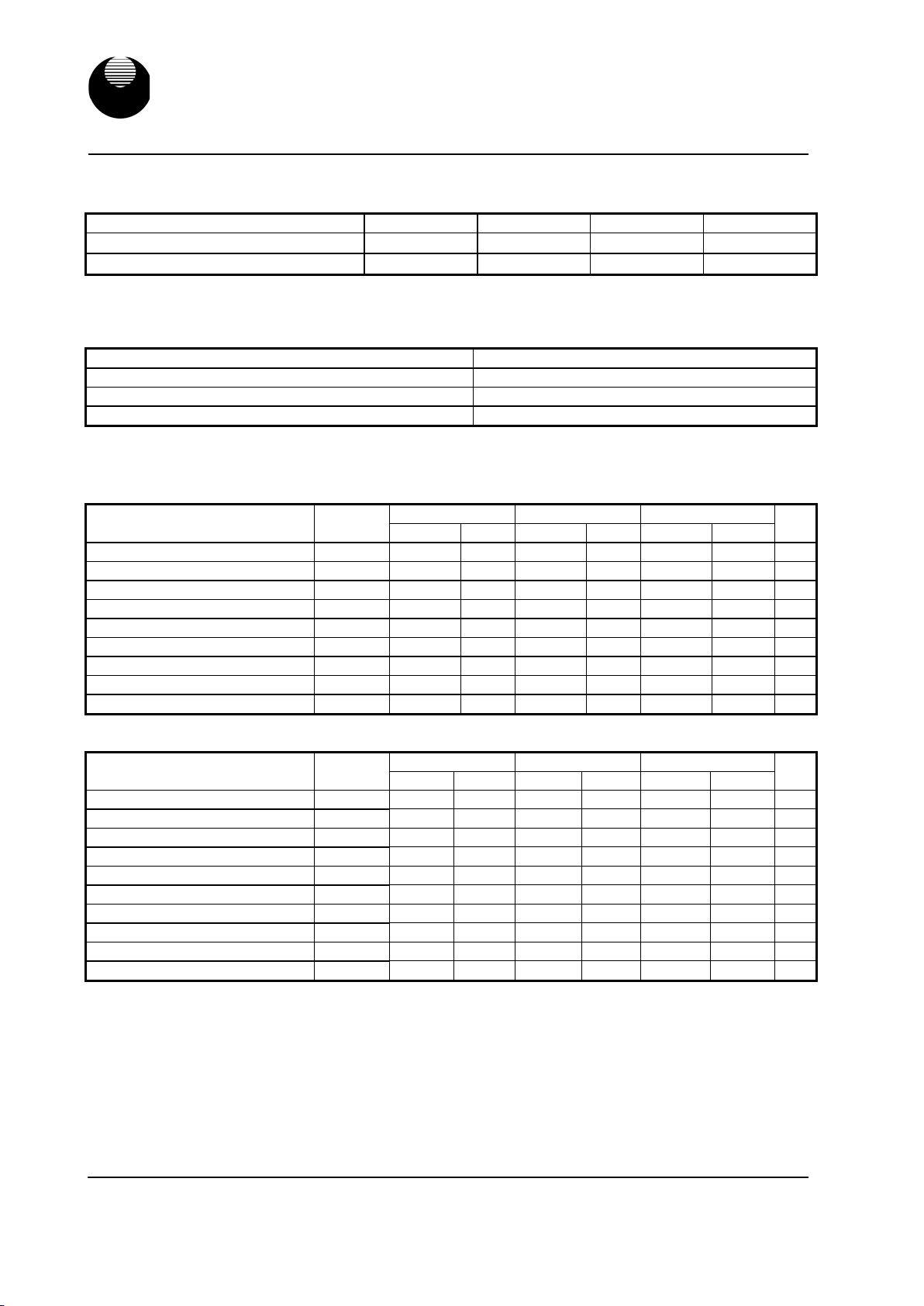
CAPACITANCE
(TA=25℃, f=1.0MHz)
PARAMETER SYMBOL MIN. MAX UNIT
Input Capacitance C
IN
-
6 pF
Input/Output Capacitance C
I/O
-
8 pF
Note : These parameters are guaranteed by device characterization, but not production tested.
AC TEST CONDITIONS
Input Pulse Levels 0V to 3.0V
Input Rise and Fall Times 5ns
Input and Output Timing Reference Levels 1.5V
Output Load CL = 30pF+1TTL , IOH/IOL = -1mA / 2.1mA
AC ELECTRICAL CHARACTERISTICS
(VCC = 2.7V~3.6V , TA = -40℃ to 85℃)
(1) READ CYCLE
UT62L5128-55 UT62L5128-70 UT62L5128-100
PARAMETER SYMBOL
MIN. MAX. MIN. MAX. MIN. MAX.
UNIT
Read Cycle Time
tRC 55 - 70 - 100 - ns
Address Access Time
tAA - 55 - 70 - 100 ns
Chip Enable Access Time
t
ACE
- 55 - 70 - 100 ns
Output Enable Access Time
tOE - 30 - 35 - 50 ns
Chip Enable to Output in Low Z
t
CLZ*
10 - 10 - 10 - ns
Output Enable to Output in Low Z
t
OLZ*
5 - 5 - 5 - ns
Chip Disable to Output in High Z
t
CHZ*
- 20 - 25 - 30 ns
Output Disable to Output in High Z
t
OHZ*
- 20 - 25 - 30 ns
Output Hold from Address Change
tOH 10 - 10 - 10 - ns
(2) WRITE CYCLE
UT62L5128-55 UT62L5128-70 UT62L5128-100
PARAMETER SYMBOL
MIN. MAX. MIN. MAX. MIN. MAX.
UNIT
Write Cycle Time
tWC 55 - 70 - 100 - ns
Address Valid to End of Write
tAW 50 - 60 - 80 - ns
Chip Enable to End of Write
tCW 50 - 60 - 80 - ns
Address Set-up Time
tAS 0 - 0 - 0 - ns
Write Pulse Width
tWP 45 - 55 - 70 - ns
Write Recovery Time
tWR 0 - 0 - 0 - ns
Data to Write Time Overlap
tDW 25 - 30 - 40 - ns
Data Hold from End of Write Time
tDH 0 - 0 - 0 - ns
Output Active from End of Write
t
OW*
5 - 5 - 5 - ns
Write to Output in High Z
t
WHZ*
- 30 - 30 - 40 ns
*These parameters are guaranteed by device characterization, but not production tested.
Page 5
UTRON
UT62L5128(I)
Preliminary Rev. 0.7
512K X 8 BIT LOW POWER CMOS SRAM
UTRON TECHNOLOGY INC. P80052
1F, No. 11, R&D Rd. II, Science-Based Industrial Park, Hsinchu, Taiwan, R. O. C.
TEL: 886-3-5777882 FAX: 886-3-5777919
5
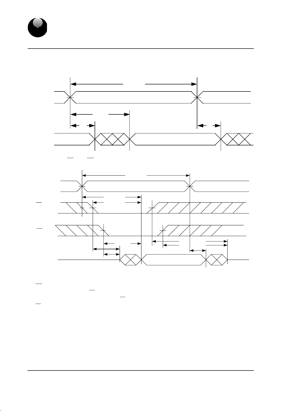
TIMING WAVEFORMS
READ CYCLE 1
(Address Controlled)
(1,2,4)
t
RC
Address
DOUT Data Valid
t
AA
t
OH
t
OH
READ CYCLE 2
(CE and
OE
Controlled)
(1,3,5,6)
t
RC
t
AA
t
ACE
t
OE
t
CHZ
t
OHZ
t
CLZ
t
OH
t
OLZ
HIGH-Z
Data Valid
HIGH-Z
Address
CE
OE
Dout
Notes :
1.
WE
is HIGH for read cycle.
2. Device is continuously selected
CE
=V
IL.
3. Address must be valid prior to or coincident with
CE
transition; otherwise t
AA
is the limiting parameter.
4.
OE
is LOW.
5. t
CLZ
, t
OLZ
, t
CHZ
and t
OHZ
are specified with CL = 5pF. Transition is measured ±500mV from steady state.
6. At any given temperature and voltage condition, t
CHZ
is less than t
CLZ
, t
OHZ
is less than t
OLZ.
Page 6

UTRON
UT62L5128(I)
Preliminary Rev. 0.7
512K X 8 BIT LOW POWER CMOS SRAM
UTRON TECHNOLOGY INC. P80052
1F, No. 11, R&D Rd. II, Science-Based Industrial Park, Hsinchu, Taiwan, R. O. C.
TEL: 886-3-5777882 FAX: 886-3-5777919
6
WRITE CYCLE 1
(WEControlled)
(1,2,3,5)
t
WC
t
AW
t
CW
t
AS
t
WP
t
WHZ
t
OW
t
DW
t
DH
t
WR
Address
CE
WE
Dout
Din
Data Valid
High-Z
(4) (4)
WRITE CYCLE 2
(
CE
Controlled)
(1,2,5)
t
WC
t
AW
t
CW
t
AS
t
WR
t
WP
t
WHZ
t
DW
t
DH
Data Valid
Address
CE
WE
Dout
Din
High-Z
Notes :
1.
WE
or
CE
must be HIGH during all address transitions.
2. A write occurs during the overlap of a low
CE
and a low
WE
.
3. During a
WE
controlled with write cycle with
OE
LOW, t
WP
must be greater than t
WHZ+tDW
to allow the drivers to turn off and
data to be placed on the bus.
4. During this period, I/O pins are in the output state, and input singals must not be applied.
5. If the
CE
low transition occurs simultaneously with or after
WE
low transition, the outputs remain in a high impedance state.
6. t
OW
and t
WHZ
are specified with CL = 5pF. Transition is measured ±500mV from steady state.
Page 7

UTRON
UT62L5128(I)
Preliminary Rev. 0.7
512K X 8 BIT LOW POWER CMOS SRAM
UTRON TECHNOLOGY INC. P80052
1F, No. 11, R&D Rd. II, Science-Based Industrial Park, Hsinchu, Taiwan, R. O. C.
TEL: 886-3-5777882 FAX: 886-3-5777919
7
DATA RETENTION CHARACTERISTICS
(TA = -40℃ to 85℃)
PARAMETER SYMBOL TEST CONDITION MIN. TYP. MAX. UNIT
Vcc for Data Retention
V
DR
CE
≧ V
CC
-0.2V
1.5 - 3.6 V
Vcc=1.5V
- L - 1 50
µ
A
Data Retention Current
I
DR
CE
≧ V
CC
-0.2V
- LL - 0.5 20
µ
A
Chip Disable to Data
t
CDR
See Data Retention
Retention Time
Waveforms (below)
0 - - ms
Recovery Time
t
R
5 - - ms
DATA RETENTION WAVEFORM
(
CE
controlled)
Data Retention Mode
V
DR
≧
1.5V
CE
≧
VCC-0.2V
V
CC
V
CC
V
IH
V
IH
V
CC
CE
t
R
t
CDR
Page 8

UTRON
UT62L5128(I)
Preliminary Rev. 0.7
512K X 8 BIT LOW POWER CMOS SRAM
UTRON TECHNOLOGY INC. P80052
1F, No. 11, R&D Rd. II, Science-Based Industrial Park, Hsinchu, Taiwan, R. O. C.
TEL: 886-3-5777882 FAX: 886-3-5777919
8
PACKAGE OUTLINE DIMENSION
32 pin 450 mil SOP Package Outline Dimension
UNIT
SYMBOL
INCH(REF) MM(BASE)
A 0.118 (MAX) 2.997 (MAX)
A1 0.004(MIN) 0.102(MIN)
A2 0.111(MAX) 2.82(MAX)
b 0.016(TYP) 0.406(TYP)
c 0.008(TYP) 0.203(TYP)
D 0.817(MAX) 20.75(MAX)
E
0.445 ±0.005 11.303 ±0.127
E1
0.555 ±0.012 14.097 ±0.305
e 0.050(TYP) 1.270(TYP)
L
0.0347 ±0.008 0.881 ±0.203
L1
0.055 ±0.008 1.397 ±0.203
S 0.026(MAX) 0.660 (MAX)
y
0.004(MAX) 0.101(MAX)
Θ
0
o
-10o 0
o
-10o
Page 9

UTRON
UT62L5128(I)
Preliminary Rev. 0.7
512K X 8 BIT LOW POWER CMOS SRAM
UTRON TECHNOLOGY INC. P80052
1F, No. 11, R&D Rd. II, Science-Based Industrial Park, Hsinchu, Taiwan, R. O. C.
TEL: 886-3-5777882 FAX: 886-3-5777919
9
32 pin STSOP Package Outline Dimension
1
16
17
32
c
L
HD
D
"A"
E
e
12
°
(2x)
12°(2x)
Seating Plane
y
32
17
16
1
c
A2A1
L
A
0.254
0
GAUGE PLANE
12°(2X)
12°(2X)
SEATING PLANE
"A" DATAIL VIEW
L1
b
UNIT
SYMBOL
INCH(BASE) MM(REF)
A 0.049 (MAX) 1.25 (MAX)
A1
0.005 ±0.002 0.130 ±0.05
A2
0.039 ±0.002 1.00 ±0.05
b
0.008 ±0.001 0.200±0.025
c 0.005 (TYP) 0.127 (TYP)
D
0.465 ±0.004 11.800 ±0.100
E
0.315 ±0.004 8.000 ±0.100
e 0.020 (TYP) 0.50 (TYP)
HD
0.528 ±0.008 13.40 ±0.20.
L
0.0197 ±0.004 0.50 ±0.10
L1
0.0315 ±0.004 0.8 ±0.10
y 0.003 (MAX) 0.076 (MAX)
Θ
0
o
〜
5
o
0
o
〜
5
o
Page 10

UTRON
UT62L5128(I)
Preliminary Rev. 0.7
512K X 8 BIT LOW POWER CMOS SRAM
UTRON TECHNOLOGY INC. P80052
1F, No. 11, R&D Rd. II, Science-Based Industrial Park, Hsinchu, Taiwan, R. O. C.
TEL: 886-3-5777882 FAX: 886-3-5777919
10
32 pin TSOP-I Package Outline Dimension
UNIT
SYMBOL
INCH(BASE) MM(REF)
A 0.047 (MAX) 1.20 (MAX)
A1
0.004 ±0.002 0.10 ±0.05
A2
0.039 ±0.002 1.00 ±0.05
b
0.008 + 0.002
- 0.001
0.20 + 0.05
-0.03
c 0.005 (TYP) 0.127 (TYP)
D
0.724 ±0.004 18.40 ±0.10
E
0.315 ±0.004 8.00 ±0.10
e 0.020 (TYP) 0.50 (TYP)
HD
0.787 ±0.008 20.00 ±0.20
L
0.0197 ±0.004 0.50 ±0.10
L1
0.0315 ±0.004 0.8 ±0.10
y 0.003 (MAX) 0.076 (MAX)
Θ
0
o
〜
5
o
0
o
〜
5
o
Page 11

UTRON
UT62L5128(I)
Preliminary Rev. 0.7
512K X 8 BIT LOW POWER CMOS SRAM
UTRON TECHNOLOGY INC. P80052
1F, No. 11, R&D Rd. II, Science-Based Industrial Park, Hsinchu, Taiwan, R. O. C.
TEL: 886-3-5777882 FAX: 886-3-5777919
11
36 pin TFBGA Package Outline Dimension
A1 Ball Pad Corner
A
B
C
D
E
F
G
H
123456
A1 Ball Pad Corner
X
Y
DETAIL A
BOTTOM VIEW ( BALL SIDE )TOP VIEW (DIE VIEW )
8.0
±
0.05
6.0±0.05
1.3755.25
1.125 3.75
0.75
0.75
SIDE VIEW
0.55
±
0.32
±
0.02
0
0.23
±
0.03
1.2 MAX.
Z
DETAIL B
0.05
0.02
SEATING PLANE
Z
DETAIL A
0.1
Z
0.08 Z
0.1 Z Y X
0.05 Z
SOLDER BALL
?0.30(x36)
1.2 MAX.
Page 12

UTRON
UT62L5128(I)
Preliminary Rev. 0.7
512K X 8 BIT LOW POWER CMOS SRAM
UTRON TECHNOLOGY INC. P80052
1F, No. 11, R&D Rd. II, Science-Based Industrial Park, Hsinchu, Taiwan, R. O. C.
TEL: 886-3-5777882 FAX: 886-3-5777919
12
ORDERING INFORMATION
PART NO. ACCESS TIME
(ns)
STANDBY CURRENT
(µA) TYP.
PACKAGE
UT62L5128SC-55LI 55 20 32 PIN SOP
UT62L5128SC-55LLI 55 3 32 PIN SOP
UT62L5128SC-70LI 70 20 32 PIN SOP
UT62L5128SC-70LLI 70 3 32 PIN SOP
UT62L5128SC-100LI 100 20 32 PIN SOP
UT62L5128SC-100LLI 100 3 32 PIN SOP
UT62L5128LS-55LI 55 20 32 PIN STSOP
UT62L5128LS-55LLI 55 3 32 PIN STSOP
UT62L5128LS-70LI 70 20 32 PIN STSOP
UT62L5128LS-70LLI 70 3 32 PIN STSOP
UT62L5128LS-100LI 100 20 32 PIN STSOP
UT62L5128LS-100LLI 100 3 32 PIN STSOP
UT62L5128LC-55LI 55 20
32 PIN TSOP-Ⅰ
UT62L5128LC-55LLI 55 3
32 PIN TSOP-Ⅰ
UT62L5128LC-70LI 70 20
32 PIN TSOP-Ⅰ
UT62L5128LC-70LLI 70 3
32 PIN TSOP-Ⅰ
UT62L5128LC-100LI 100 20
32 PIN TSOP-Ⅰ
UT62L5128LC-100LLI 100 3
32 PIN TSOP-Ⅰ
UT62L5128BS-55LI 55 20 36 PIN TFBGA
UT62L5128BS-55LLI 55 3 36 PIN TFBGA
UT62L5128BS-70LI 70 20 36 PIN TFBGA
UT62L5128BS-70LLI 70 3 36 PIN TFBGA
UT62L5128BS-100LI 100 20 36 PIN TFBGA
UT62L5128BS-100LLI 100 3 36 PIN TFBGA
Page 13

UTRON
UT62L5128(I)
Preliminary Rev. 0.7
512K X 8 BIT LOW POWER CMOS SRAM
UTRON TECHNOLOGY INC. P80052
1F, No. 11, R&D Rd. II, Science-Based Industrial Park, Hsinchu, Taiwan, R. O. C.
TEL: 886-3-5777882 FAX: 886-3-5777919
13
REVISION HISTORY
REVISION DESCRIPTION DATE
Preliminary Rev. 0.5 Original. Mar, 2001
Preliminary Rev. 0.6
1. The symbols CE# and OE# and WE# are revised as.
CE
and
OE and
WE
.
2. Separate Industrial and Consumer SPEC.
3. Add access time 55ns range.
Jun 21,2001
Preliminary Rev. 0.7
1. Add SOP and STSOP package
Dec 18,2001
Page 14

UTRON
UT62L5128(I)
Preliminary Rev. 0.7
512K X 8 BIT LOW POWER CMOS SRAM
UTRON TECHNOLOGY INC. P80052
1F, No. 11, R&D Rd. II, Science-Based Industrial Park, Hsinchu, Taiwan, R. O. C.
TEL: 886-3-5777882 FAX: 886-3-5777919
14
THIS PAGE IS LEFT BLANK INTENTIONALLY.
 Loading...