

Page 1
UT54ACTS220
Clock and Wait-State Generation Circuit
FEATURES
• 1.2µ radiation-hardened CMOS
- Latchup immune
• High speed
• Low power consumption
• Single 5-volt supply
• Available QML Q or V processes
• Flexible package
- 14-pin DIP
- 14-lead flatpack
DESCRIPTION
The UT54ACTS220 is designed to be a companion chip to
UTMC’s UT69151 SµMMIT family for the purpose of generating clock and wait-state signals. The device contains a divide
by two circuit that accepts TTL input levels and drives CMOS
output buffers. The chip accepts a 48MHz clock and generates
a 24MHz clock. The 48MHz clock can have a duty cycle that
varies by ± 20%. The UT54ACT220 generates a 24MHz clock
with a ± 5% duty cycle variation. The wait-state circuit generates
a single wait-state by delaying the falling edge of DTACK into
the SµMMIT. The clock/timing device generates DTACK from
the falling edge of input RCS which is synchronized by the
falling edge of 24MHz. The SµMMIT drives inputs RCS and
DMACK.
The devices are characterized over full military temperature
range of -55°C to +125°C.
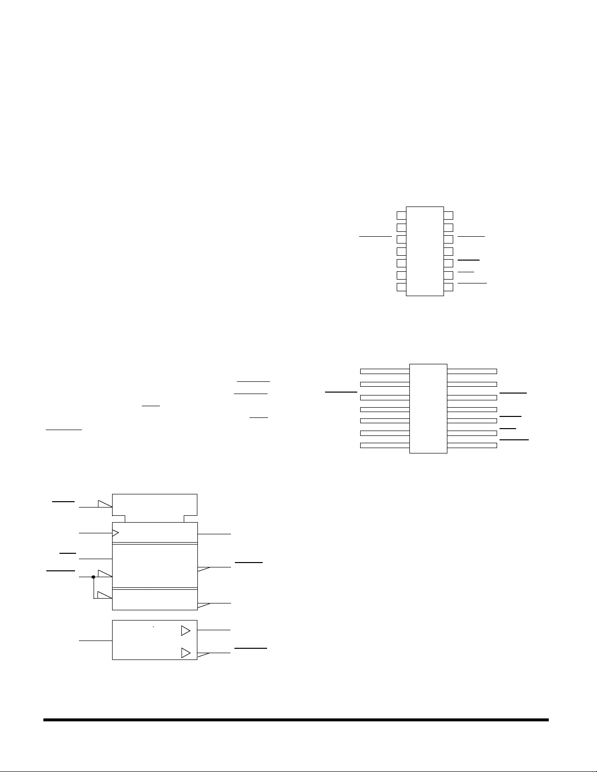
LOGIC SYMBOL
PINOUTS
CLKOUT
CLKOUT
CLKIN
48MHz
V
NC
NC
SS
NC
CLKOUT
CLKOUT
CLKIN
NC
48MHz
V
14-Pin DIP
Top View
1 14
2 13
3 12
4 11
5 10
6 9
7 8
SS
14-Lead Flatpack
Top View
1 14
2 13
3 12
4 11
5 10
6 9
7 8
V
DD
24MHz
DTACK
TEST
MRST
RCS
DMACK
V
DD
24MHz
DTACK
TEST
MRST
RCS
DMACK
(10)
MRST
RCS
CLKIN
(6)
(9)
(8)
(4)
48MHz
DMACK
Note:
1. Logic symbol in accordance with ANSI/IEEE Std 91-1984 and IEC
Publication 617-12.
S
1D
S
CTR1
SRG2
(13)
(12)
(11)
(2)
(3)
24MHz
DTACK
TEST
CLKOUT
CLKOUT
145 RadHard MSI Logic
Page 2
PIN DESCRIPTION
Pin Number Pin Name Description
2 CLKOUT Buffered version of CLKIN.
3 CLKOUT Inverted version of CLKIN.
4 CLKIN Clock Input. This signal can be any arbitrary signal that the user wishes to buffer.
6 48MHz 48MHz Clock. The 24MHz clock is created by dividing this signal by two.
8 DMACK DMA Acknowledge. This input is generated by the SµMMIT. When high, this signal
will cause DTACK output to be forced high.
9 RCS RAM Chip Select. This input is generated by the SµMMIT.
UT54ACTS220
10 MRST Master Reset. This input can be used to preset 24MHz, DTACK and TEST. For normal
11 TEST Test output signal.
12 DTACK Data Transfer Acknowledge. This signal can be used to drive the DTACK signal of the
13 24MHz 24MHz Clock. This output runs at half the frequency of the 48MHz input. The falling
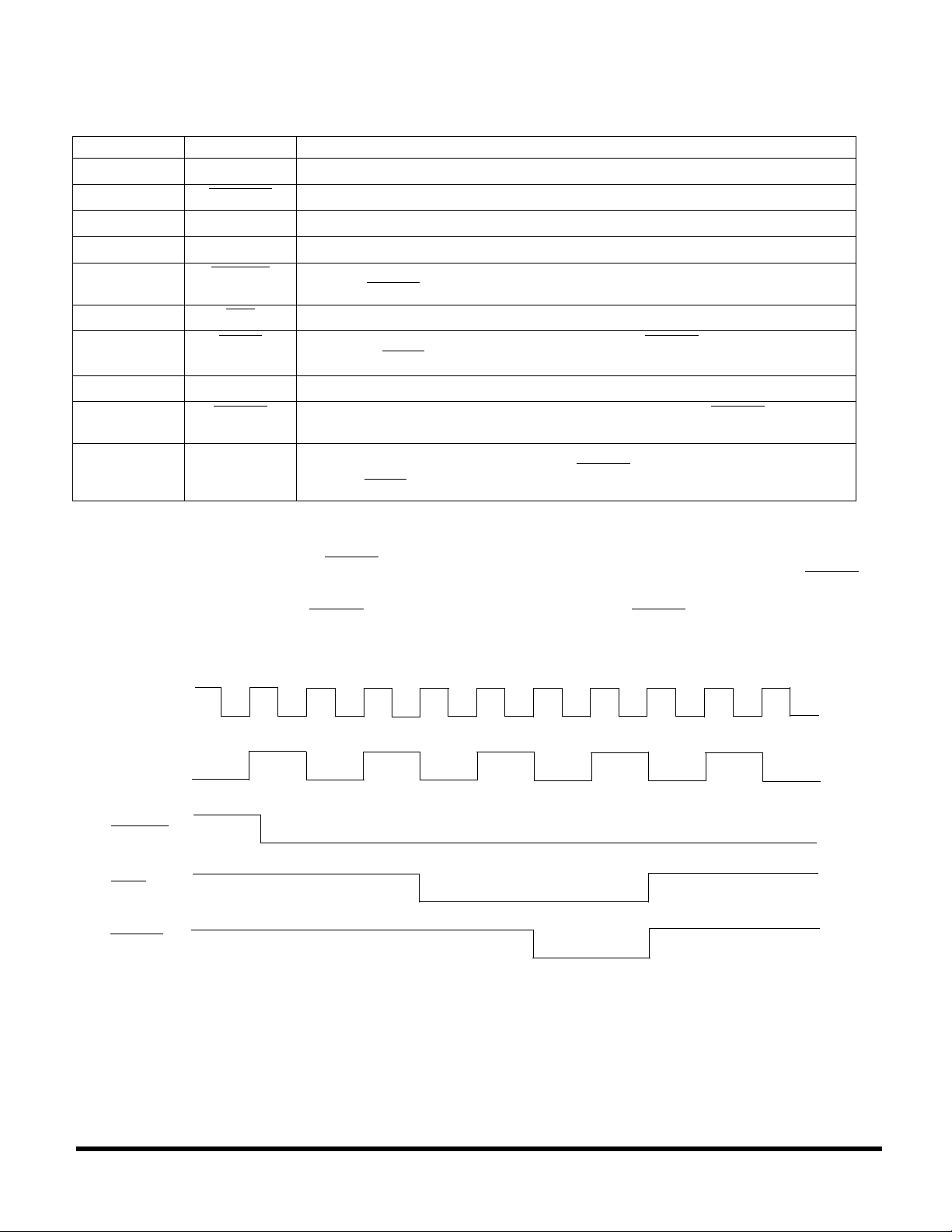
FUNCTIONAL TIMING: Single SµMMIT Wait-State
For both read and write memory cycles, DTACK is an input to the SµMMIT E and SµMMIT LXE/DXE. A non-wait state mem-
ory requires two clock cycles, T1 and T2 of figure 1. For accessing slower memory devices, the UT54ACTS220 holds DTACK to
a logical “1”. This results in the stretching of memory cycles by one clock to three clock cycles, TW of figure 1. The SµMMIT E
and SµMMIT LXE/DXE samples the DTACK on the rising edge of the 24 MHz clock. If DTACK is not generated before the ris-
ing edge of the clock, the SµMMIT E and SµMMIT LXE/DXE extends the memory cycle.
48MHz
24MHz
operation tie MRST to VDD through a resistor.
SµMMIT if the user requires one wait state during the memory transfer.
edge of 24MHz is the signal that latches the DTACK outputs. 24MHz is forced high
whenever MRST is low. Properly loaded, 24MHz will have a 50% duty cycle ± 5%.
T
1
T
W
T
2
DMACK
RCS
DTACK
Figure 1. Functional Timing
RadHard MSI Logic 146
Page 3
UT54ACTS220
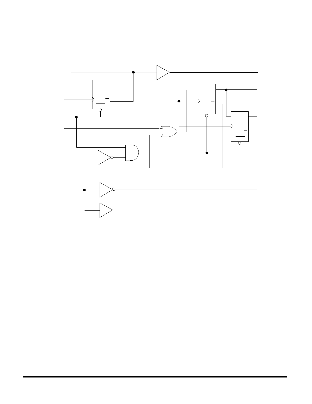
LOGIC DIAGRAM
24MHz
D
Q
Q
D
DTACK
48MHz
MRST
RCS
DMACK
CLKIN
CK
RST
Q
CK
PRE
Q
Q
D
CK
Q
PRE
TEST
CLKOUT
CLKOUT
147 RadHard MSI Logic
Page 4

RADIATION HARDNESS SPECIFICATIONS
PARAMETER LIMIT UNITS
Total Dose 1.0E6 rad(Si)
UT54ACTS220
SEU Threshold
1
SEL Threshold >120
Neutron Fluence
Notes:
1. Device storage elements are immune to SEU affects.
2. Not tested, inherent of CMOS technology.
2
ABSOLUTE MAXIMUM RATINGS
SYMBOL PARAMETER LIMIT UNITS
V
DD
V
I/O
T
STG
T
T
Θ
P
J
LS
JC
I
I
D
Storage Temperature range -65 to +150 °C
Maximum junction temperature +175 °C
Lead temperature (soldering 5 seconds) +300 °C
Thermal resistance junction to case 20 °C/W
Maximum power dissipation 1 W
80
MeV-cm2/mg
MeV-cm2/mg
1.0E14
n/cm
2
Supply voltage -0.3 to 7.0 V
Voltage any pin -0.3 to VDD +0.3 V
DC input current ±10 mA
Note:
1.Stresses outside the listed absolute maximum ratings may cause permanent damage to the device. This is a stress rating only, functional operation of the device
at these or any other conditions beyond limits indicated in the operational sections is not recommended. Exposure to absolute maximum rating conditions for
extended periods may affect device reliability.
RECOMMENDED OPERATING CONDITIONS
SYMBOL PARAMETER LIMIT UNITS
V
DD
V
IN
T
C
Supply voltage 4.5 to 5.5 V
Input voltage any pin 0 to V
DD
Temperature range -55 to + 125 °C
V
48MHz Duty Cycle 50 ± 20% MHz
RadHard MSI Logic 148
Page 5

UT54ACTS220
DC ELECTRICAL CHARACTERISTICS
(V
= 5.0V ±10%; V
DD
= 0V 6, -55°C < TC < +125°C)
SS
7
SYMBOL PARAMETER CONDITION MIN MAX UNIT
V
IL
Low-level input voltage
TTL
V
IH High-level input voltage
TTL
I
IN
Input leakage current
TTL
V
OL1
Low-level output voltage
Except CLKOUT/CLKOUT
V
OH1 High-level output voltage
1
0.8 V
1
2.25 V
V
= 5.5V
DD
VIN = V
3
3
IOL = 8mA, V
I
= 100µA
OL
IOH = -8mA, V
DD
or V
SS
= 4.5V
DD
= 4.5V 3.15
DD
-1
1 µA
0.4
0.25 V
Except CLKOUT/CLKOUT
V
V
OL2
OH2
CLKOUT/CLKOUT Low-level output
voltage
3
CLKOUT/CLKOUT High-level output
I
= 100µA 0.25
OL
I
= -100µA 4.25
OH
voltage 3
I
OS
Short-circuit output current
2 ,4
VO = VDD and V
V
= 5.5V
DD
SS
+300 mA
V
V
V
I
OL1
Output current
(Sink), Except CLKOUT/CLKOUT
I
OH1 Output current
(Source), Except CLKOUT/CLKOUT
I
OL2
CLKOUT/CLKOUT output current
(Sink)
I
OH2
CLKOUT/CLKOUT output current
(Source)
I
I
P
total
I
DDQ
IH
IL
Input current high
Input current low
Power dissipation
Quiescent Supply Current VDD = 5.5V
10
10
2, 8, 9
10
10
VIN = VDD or V
SS
8 mA
VOL = 0.4V
VIN = VDD or V
SS
-8 mA
VOH = VDD - 0.4V
VIN = VDD or V
SS
12 mA
VOL = 0.4V
VIN = VDD or V
SS
-12 mA
VOH = VDD - 0.4V
VIN = VDD or V
V
= 5.5V
IN
VIN = VDD or V
V
= V
IN
SS
SS
SS
+1.0 µA
-1.0 µA
CL = 50pF 1.0 mW/
MHz
10 µA
V
IN = VDD or VSS
149 RadHard MSI Logic
Page 6

UT54ACTS220
∆I
DDQ
Quiescent Supply Current Delta
For input under test
VIN = VDD - 2.1V
1.6 mA
For all other inputs
VIN = VDD or V
V
= 5.5V
DD
C
IN
C
OUT Output capacitance
Notes:
1. Functional tests are conducted in accordance with MIL-STD-883 with the following input test conditions: VIH = VIH(min) + 20%, - 0%; VIL = VIL(max) + 0%,
- 50%, as specified herein, for TTL, CMOS, or Schmitt compatible inputs. Devices may be tested using any input voltage within the above specified range, but
are guaranteed to VIH(min) and VIL(max).
2. Supplied as a design limit but not guaranteed or tested.
3. Per MIL-PRF-38535, for current density ≤5.0E5 amps/cm2, the maximum product of load capacitance (per output buffer) times frequency should not exceed
3,765 pF/MHz.
4. Not more than one output may be shorted at a time for maximum duration of one second.
5. Capacitance measured for initial qualification and when design changes may affect the value. Capacitance is measured between the designated terminal and VSS
at frequency of 1MHz and a signal amplitude of 50mV rms maximum.
6. Maximum allowable relative shift equals 50mV.
7. All specifications valid for radiation dose ≤ 1E6 rads(Si).
8. Power does not include power contribution of any TTL output sink current.
9. Power dissipation specified per switching output.
10. This value is guaranteed based on characterization data, but not tested.
Input capacitance
5
5
ƒ = 1MHz @ 0V 15 pF
ƒ = 1MHz @ 0V 15 pF
SS
RadHard MSI Logic 150
Page 7

UT54ACTS220
AC ELECTRICAL DIAGRAM
48MHz
24MHz
RCS
DTACK
CLKIN
CLKOUT
or
CLKOUT
T
1
t
SUR
T
W
t
PHL
t
SU
or t
PLH
T
W
t
H
T
2
151 RadHard MSI Logic
Page 8

UT54ACTS220
AC ELECTRICAL CHARACTERISTICS
(V
= 5.0V ±10%; V
DD
= 0V1, -55°C < TC < +125°C)
SS
2
SYMBOL PARAMETER MINIMUM MAXIMUM UNIT
t
1 48MHz ↑ to 24MHz ↓ 0 15 ns
PHL
t
1 48MHz ↑ to 24MHz ↑ 0 15 ns
PLH
t
2 24MHz ↓ to DTACK ↓ 0 7 ns
PHL
t
2 24MHz ↓ to DTACK ↑ 0 6 ns
PLH
t
3 DMACK ↑ to DTACK ↑ 3 16 ns
PLH
t
4 MRST ↓ to 24MHz ↑, DTACK ↑ 3 16 ns
PLH
t
5 CLKIN ↓ to CLKOUT ↓ 0 11 ns
PHL
t
5 CLKIN ↑ to CLKOUT ↑ 0 11 ns
PLH
t
6 CLKIN ↑ to CLKOUT ↓ 0 11 ns
PHL
t
6 CLKIN ↓ to CLKOUT ↑ 0 11 ns
PLH
3
t
SU
3
t
H
DTACK ↓ to 24MHz ↑, setup time 12 ns
24MHz ↑ to DTACK ↑, hold time 20 ns
t
SUR
t
WM
t
WC
f
MAX
Notes:
1. Maximum allowable relative shift equals 50mV.
2. All specifications valid for radiation dose ≤ 1E6 rads(Si).
3. Guaranteed by design but not tested.
Setup time from RCS ↓ to 24MHz ↓ 7 ns
MRST pulse width low 5 ns
CLKIN pulse width 12 ns
Maximum CLKIN frequency 40 MHz
RadHard MSI Logic 152
 Loading...