

Page 1
137 RadHard MSI Logic
UT54ACS193/UT54ACTS193
Radiation-Hardened
Synchronous 4-Bit Up-Down Dual Clock Counters
FEATURES
Look-ahead circuitry enhances cascaded counters
Fully synchronous in count modes
Asynchronous clear
radiation-hardened CMOS
- Latchup immune
High speed
Low power consumption
Single 5 volt supply
Available QML Q or V processes
Flexible package
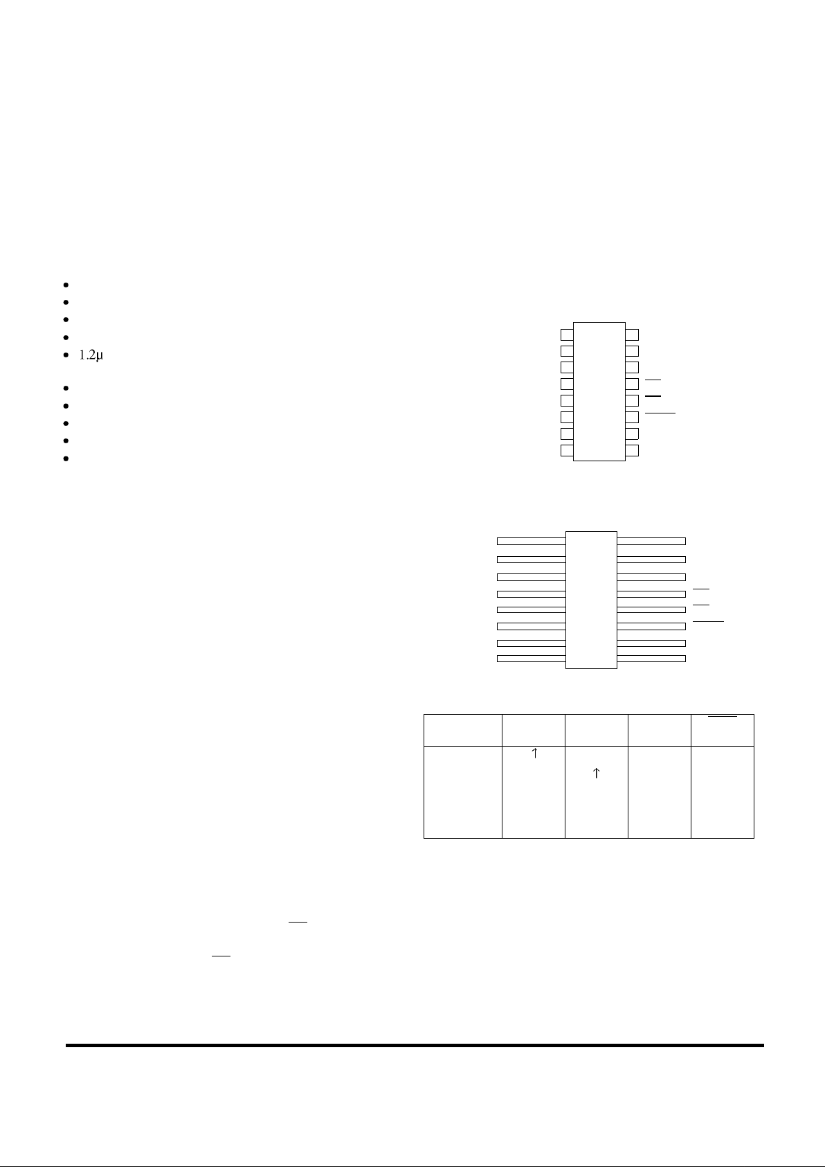
16-pin DIP
-
DESCRIPTION
The UT54ACS193 and the UT54ACTS193 are synchronous 4-
operation is provided by having all flip-flops clocked
simultaneously so that the outputs change coincident with each
output counting spikes normally associated with asynchronous
counters.
level transition of either count input (Up or Down). The direction of the counting is determined by which count input is pulsed
The counters are fully programmable. The outputs may be preset to either level by placing a low on the load input and entering
agree with the data inputs independently of the count pulses.
Asynchronous loading allows the counters to be used as modu-
preset inputs.
A clear input has been provided that forces all outputs to the low
pendent of the count and the load inputs.
The counter is designed for efficient cascading without the need
BO) produces a low-
Similarly, the carry output (CO
while the count is maximum
PINOUTS
Top View
16-Lead Flatpack
FUNCTION TABLE
FUNCTION CLOCK UPCLOCK
DOWN
CLR LOAD
Count Up H L H
Count Down H L H
Reset X X H X
Load Preset
Input
X X L L
1
2
3
4
5
7
6
16
15
14
13
12
10
11
B
Q
B
Q
A
DOWN
UP
Q
C
Q
D
V
DD
A
CLR
BO
CO
C
8 9
V
SS
D
LOAD
1
2
3
4
5
7
6
16
15
14
13
12
10
11
V
DD
8 9
B
Q
B
Q
A
DOWN
UP
Q
C
Q
D
A
CLR
BO
CO
LOAD
C
V
SS
D
Page 2
RadHard MSI Logic 138
UT54ACS193/UT54ACTS193
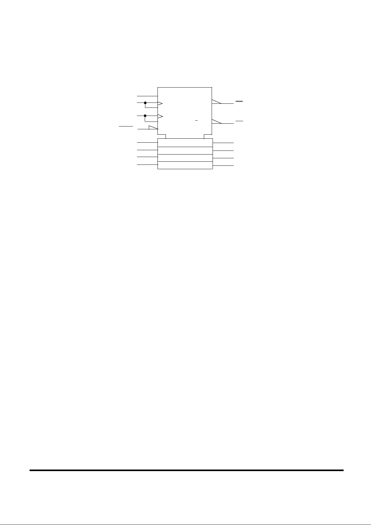
LOGIC SYMBOL
(14)
CLR
(5)
UP
G1
CT=0
CTRDIV 16
(4)
DOWN
(15)
A
(1)
B
(10)
C
(9)
D
(12)
(3)
Q
A
(7)
Q
D
(6)
Q
C
(2)
Q
B
3D
(1)
(2)
(4)
(8)
2+
G2
(11)
LOAD C3
(13)
BO
2CT=0
1-
CO
1CT=15
Note:
1. Logic symbol in accordance with ANSI/IEEE Std 91-1984 and IEC Publication 617-12.
Page 3
139 RadHard MSI Logic
UT54ACS193/UT54ACTS193
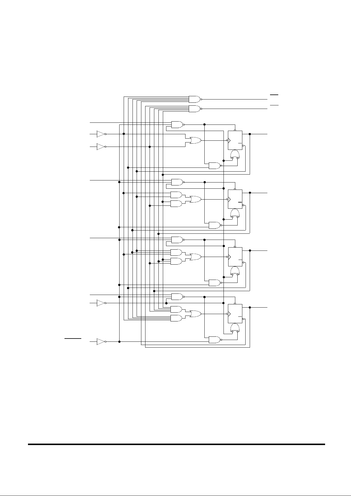
LOGIC DIAGRAM
A
DOWN
UP
CLR
LOAD
(15)
(4)
(5)
(1)
(10)
(9)
(14)
(11)
Q
(7)
(6)
(2)
(3)
(12)
(13)
B
C
D
BO
CO
D
C
B
A
Q
Q
Q
C
Q
R
S
Q
C
Q
R
S
Q
C
Q
R
S
Q
C
Q
R
S
Q
Page 4

RadHard MSI Logic 140
UT54ACS193/UT54ACTS193
RADIATION HARDNESS SPECIFICATIONS
1
Notes:
1. Logic will not latchup during radiation exposure within the limits defined in the table.
2. Device storage elements are immune to SEU affects.
ABSOLUTE MAXIMUM RATINGS
Note:
1. Stresses outside the listed absolute maximum ratings may cause permanent damage to the device. This is a stress rating only, functional operation of the device
at these or any other conditions beyond limits indicated in the operational sections is not recommended. Exposure to absolute maximum rating conditions for
extended periods may affect device reliability.
PARAMETER LIMIT UNITS
Total Dose 1.0E6 rads(Si)
SEU Threshold
2
80
MeV-cm2/mg
SEL Threshold 120
MeV-cm2/mg
Neutron Fluence 1.0E14
n/cm
2
SYMBOL PARAMETER LIMIT UNITS
V
DD
Supply voltage -0.3 to 7.0 V
V
I/O
Voltage any pin -.3 to VDD +.3 V
T
STG
Storage Temperature range -65 to +150 C
T
J
Maximum junction temperature +175 C
T
LS
Lead temperature (soldering 5 seconds) +300 C
JC
Thermal resistance junction to case 20 C/W
I
I
DC input current 10 mA
P
D
Maximum power dissipation 1 W
Page 5

141 RadHard MSI Logic
UT54ACS193/UT54ACTS193
RECOMMENDED OPERATING CONDITIONS
SYMBOL PARAMETER LIMIT UNITS
V
DD
Supply voltage 4.5 to 5.5 V
V
IN
Input voltage any pin 0 to V
DD
V
T
C
Temperature range -55 to + 125 C
Page 6

RadHard MSI Logic 142
UT54ACS193/UT54ACTS193
DC ELECTRICAL CHARACTERISTICS
7
(VDD = 5.0V 10%; VSS = 0V 6, -55 C < TC < +125 C)
SYMBOL PARAMETER CONDITION MIN MAX UNIT
V
IL
Low-level input voltage
1
ACTS
ACS
0.8
.3V
DD
V
V
IH
High-level input voltage
1
ACTS
ACS
.5V
DD
.7V
DD
V
I
IN
Input leakage current
ACTS/ACS VIN = V
DD
or V
SS
-1
1 A
V
OL
Low-level output voltage
3
ACTS
ACS
I
OL
= 8.0mA
I
OL
= 100 A
0.40
0.25
V
V
OH
High-level output voltage
3
ACTS
ACS
I
OH
= -8.0mA
I
OH
= -100 A
.7V
DD
VDD - 0.25
V
I
OS
Short-circuit output current
2 ,4
ACTS/ACS
VO = VDD and V
SS
-200 200 mA
I
OL Output current
10
(Sink)
VIN = VDD or V
SS
VOL = 0.4V
8 mA
I
OH
Output current
10
(Source)
VIN = VDD or V
SS
VOH = VDD - 0.4V
-8 mA
P
total
Power dissipation
2, 8, 9
CL = 50pF 2.1 mW/
MHz
I
DDQ
Quiescent Supply Current VDD = 5.5V 10 A
I
DDQ
Quiescent Supply Current Delta
ACTS
For input under test
VIN = VDD - 2.1V
For all other inputs
VIN = VDD or V
SS
V
DD
= 5.5V
1.6 mA
C
IN
Input capacitance
5
= 1MHz @ 0V 15 pF
C
OUT
Output capacitance 5
= 1MHz @ 0V 15 pF
Page 7

143 RadHard MSI Logic
UT54ACS193/UT54ACTS193
Notes:
1. Functional tests are conducted in accordance with MIL-STD-883 with the following input test conditions: VIH = VIH(min) + 20%, - 0%; VIL = VIL(max) + 0%,
- 50%, as specified herein, for TTL, CMOS, or Schmitt compatible inputs. Devices may be tested using any input voltage within the above specified range, but
are guaranteed to VIH(min) and VIL(max).
2. Supplied as a design limit but not guaranteed or tested.
3. Per MIL-PRF-38535, for current density 5.0E5 amps/cm2, the maximum product of load capacitance (per output buffer) times frequency should not exceed
3,765 pF/MHz.
4. Not more than one output may be shorted at a time for maximum duration of one second.
5. Capacitance measured for initial qualification and when design changes may affect the value. Capacitance is measured between the designated terminal and VSS
at frequency of 1MHz and a signal amplitude of 50mV rms maximum.
6. Maximum allowable relative shift equals 50mV.
7. All specifications valid for radiation dose 1E6 rads(Si).
8. Power does not include power contribution of any TTL output sink current.
9. Power dissipation specified per switching output.
10. This value is guaranteed based on characterization data, but not tested.
Page 8

RadHard MSI Logic 144
UT54ACS193/UT54ACTS193
AC ELECTRICAL CHARACTERISTICS
2
(VDD = 5.0V 10%; VSS = 0V 1, -55 C < TC < +125 C)
Notes:
1. Maximum allowable relative shift equals 50mV.
2. All specifications valid for radiation dose 1E6 rads(Si).
3. Based on characterization, data hold time (tH3) of 0ns can be assumed if data setup time (t
SU3
) is >10ns. This is guaranteed, but not tested.
SYMBOL PARAMETER MINIMUM MAXIMUM UNIT
t
PLH
UP to Q
n
2 20 ns
t
PHL
UP to Q
n
2 24 ns
t
PLH
UP to CO 2 13 ns
t
PHL
UP to CO 2 16 ns
t
PLH
DOWN to BO 2 13 ns
t
PHL
DOWN to BO 2 16 ns
t
PLH
DOWN to Q
n
2 20 ns
t
PHL
DOWN to Q
n
2 24 ns
t
PLH
LOAD to Q
n
2 22 ns
t
PHL
LOAD to Q
n
2 23 ns
t
PHL
CLR to Q
n
2 22 ns
f
MAX
Maximum clock frequency 56 MHz
t
SU1
LOAD inactive setup time before UP or DOWN 3 ns
t
SU2
CLR inactive setup time before UP or DOWN 3 ns
t
SU3
A, B, C, D setup time before LOAD 6 ns
t
H1
UP high hold time after DOWN 20 ns
t
H2
DOWN high hold time after UP 20 ns
t
H3
3
A, B, C, D hold time after LOAD 2 ns
t
W
Minimum pulse width
UP high or low
DOWN high or low
LOAD low
CLR high
9 ns
 Loading...