

Page 1
217 RadHard MSI Logic
UT54ACS373/UT54ACTS373
Radiation-Hardened
Octal Transparent Latches with Three-State Outputs
FEATURES
8 latches in a single package
Three-state bus-driving true outputs
Full parallel access for loading
radiation-hardened CMOS
- Latchup immune
High speed
Low power consumption
Single 5 volt supply
Available QML Q or V processes
Flexible package
- 20-pin DIP
- 20-lead flatpack
DESCRIPTION
The UT54ACS373 and the UT54ACTS373 are 8-bit latches
with three-state outputs designed for driving highly capacitive
or relatively low-impedance loads. The device is suitable for
buffer registers, I/O ports, and bidirectional bus drivers.
The eight latches are transparent D latches. While the enable
(C) is high the Q outputs will follow the data (D) inputs. When
the enable is taken low, the Q outputs will be latched at the levels
that were set up at the D inputs.
An output-control input (OC) places the eight outputs in either
a normal logic state (high or low logic levels) or a high-impedance state. The high-impedance third state and increased drive
provide the capability to drive the bus line in a bus-organized
system without need for interface or pull-up components.
The output control OC does not affect the internal operations of
the latches. Old data can be retained or new data can be entered
while the outputs are off.
The devices are characterized over full military temperature
range of -55 C to +125 C.
FUNCTION TABLE
Note:
1. Data may be latched internally.
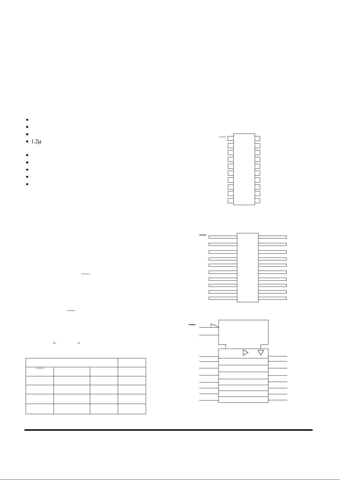
PINOUTS
20-Pin DIP
Top View
20-Lead Flatpack
Top View
LOGIC SYMBOL
INPUTS OUTPUT
OC C nD nQ
L H H H
L H L L
L L X nQ
0
H X X
Z
1
1
2
3
4
5
7
6
20
19
18
17
16
14
15
OC
1Q
1D
2D
2Q
3Q
3D
V
DD
8Q
8D
7D
7Q
6D
8 134D 5D
6Q
9 124Q 5Q
10 11V
SS
C
1
2
3
4
5
7
6
20
19
18
17
16
14
15
OC
1Q
1D
2D
2Q
3Q
3D
V
DD
8Q
8D
7D
7Q
6D
8 134D 5D
6Q
9 124Q 5Q
10 11V
SS
C
(1)
OC EN
(3)
1D
(4)
2D
(7)
(2)
1Q
(6)
(5)
2Q
Note:
1. Logic symbol in accordance with ANSI/IEEE Std 91-1984 and IEC
Publication 617-12.
3D
(8)
4D
(13)
5D
(14)
6D
3Q
(15)
6Q
(12)
5Q
(9)
4Q
(17)
7D
(18)
8D
(19)
8Q
(16)
7Q
(11)
C C1
1D
Page 2
RadHard MSI Logic 218
UT54ACS373/UT54ACTS373
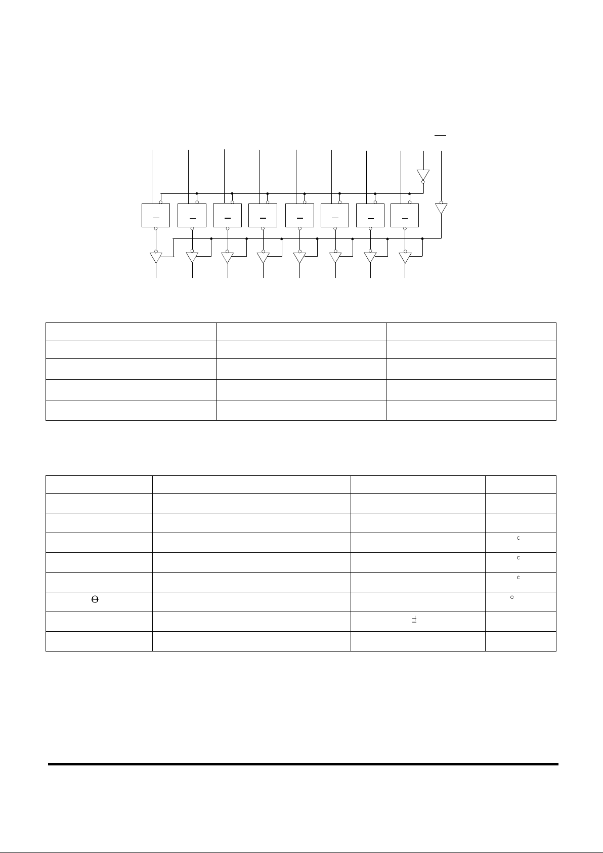
LOGIC DIAGRAM
RADIATION HARDNESS SPECIFICATIONS
1
Notes:
1. Logic will not latchup during radiation exposure within the limits defined in the table.
2. Device storage elements are immune to SEU affects.
ABSOLUTE MAXIMUM RATING
Note:
1. Stresses outside the listed absolute maximum ratings may cause permanent damage to the device. This is a stress rating only, functional operation of the device
at these or any other conditions beyond limits indicated in the operational sections is not recommended. Exposure to absolute maximum rating conditions for
extended periods may affect device reliability.
PARAMETER LIMIT UNITS
Total Dose 1.0E6 rads(Si)
SEU Threshold
2
80
MeV-cm2/mg
SEL Threshold 120
MeV-cm2/mg
Neutron Fluence 1.0E14
n/cm
2
OC
C
1D2D3D4D5D6D7D8D
(1)
(11)
(4)(7)(8)
(13)(14)(17)(18)
(2)(5)(6)(9)(12)(15)(16)(19)
1Q2Q3Q4Q5Q6Q7Q8Q
CD
CDCD
CD
C
D
CD
(3)
D CCD
Q
Q
Q
Q
Q
Q
Q Q
SYMBOL PARAMETER LIMIT UNITS
V
DD
Supply voltage -0.3 to 7.0 V
V
I/O
Voltage any pin -.3 to VDD +.3 V
T
STG
Storage Temperature range -65 to +150 C
T
J
Maximum junction temperature +175 C
T
LS
Lead temperature (soldering 5 seconds) +300 C
JC
Thermal resistance junction to case 20 C/W
I
I
DC input current 10 mA
P
D
Maximum power dissipation 1 W
Page 3

219 RadHard MSI Logic
UT54ACS373/UT54ACTS373
RECOMMENDED OPERATING CONDITIONS
SYMBOL PARAMETER LIMIT UNITS
V
DD
Supply voltage 4.5 to 5.5 V
V
IN
Input voltage any pin 0 to V
DD
V
T
C
Temperature range -55 to + 125 ×C
Page 4

RadHard MSI Logic 220
UT54ACS373/UT54ACTS373
DC ELECTRICAL CHARACTERISTICS
7
(VDD = 5.0V 10%; VSS = 0V 6, -55 C < TC < +125 C)
SYMBOL PARAMETER CONDITION MIN MAX UNIT
V
IL
Low-level input voltage
1
ACTS
ACS
0.8
.3V
DD
V
V
IH
High-level input voltage
1
ACTS
ACS
.5V
DD
.7V
DD
V
I
IN
Input leakage current
ACTS/ACS VIN = V
DD
or V
SS
-1
1 A
V
OL
Low-level output voltage
3
ACTS
ACS
I
OL
= 8.0mA
I
OL
= 100 A
0.40
0.25
V
V
OH
High-level output voltage
3
ACTS
ACS
I
OH
= -8.0mA
I
OH
= -100 A
.7V
DD
VDD - 0.25
V
I
OZ
Three-state output leakage current VO = VDD and V
SS
-20 20 A
I
OS Short-circuit output current
2 ,4
ACTS/ACS
VO = VDD and V
SS
-200 200 mA
I
OL
Output current
10
(Sink)
VIN = VDD or V
SS
VOL = 0.4V
8 mA
I
OH
Output current
10
(Source)
VIN = VDD or V
SS
VOH = VDD - 0.4V
-8 mA
P
total
Power dissipation
2, 8, 9
CL = 50pF 1.9 mW/
MHz
I
DDQ
Quiescent Supply Current VDD = 5.5V 10 A
I
DDQ
Quiescent Supply Current Delta
ACTS
For input under test
VIN = VDD - 2.1V
For all other inputs
VIN = VDD or V
SS
V
DD
= 5.5V
1.6 mA
C
IN Input capacitance
5
= 1MHz @ 0V 15 pF
C
OUT
Output capacitance 5
= 1MHz @ 0V 15 pF
Page 5

221 RadHard MSI Logic
UT54ACS373/UT54ACTS373
Notes:
1. Functional tests are conducted in accordance with MIL-STD-883 with the following input test conditions: VIH = VIH(min) + 20%, - 0%; VIL = VIL(max) + 0%,
- 50%, as specified herein, for TTL, CMOS, or Schmitt compatible inputs. Devices may be tested using any input voltage within the above specified range, but
are guaranteed to VIH(min) and VIL(max).
2. Supplied as a design limit but not guaranteed or tested.
3. Per MIL-PRF-38535, for current density 5.0E5 amps/cm2, the maximum product of load capacitance (per output buffer) times frequency should not exceed
3,765 pF/MHz.
4. Not more than one output may be shorted at a time for maximum duration of one second.
5. Capacitance measured for initial qualification and when design changes may affect the value. Capacitance is measured between the designated terminal and VSS
at frequency of 1MHz and a signal amplitude of 50mV rms maximum.
6. Maximum allowable relative shift equals 50mV.
7. All specifications valid for radiation dose 1E6 rads(Si).
8. Power does not include power contribution of any TTL output sink current.
9. Power dissipation specified per switching output.
10. This value is guaranteed based on characterization data, but not tested.
Page 6

RadHard MSI Logic 222
UT54ACS373/UT54ACTS373
AC ELECTRICAL CHARACTERISTICS
2
(VDD = 5.0V 10%; VSS = 0V 1, -55 C < TC < +125 C)
Notes:
1. Maximum allowable relative shift equals 50mV.
2. All specifications valid for radiation dose 1E6 rads(Si).
SYMBOL PARAMETER MINIMUM MAXIMUM UNIT
t
PLH
Data to Qn 1 14 ns
t
PHL
Data to Qn 1 16 ns
t
PLH
C to Qn 1 16 ns
t
PHL
C to Qn 1 18 ns
t
PZL
OC low to Qn 1 14 ns
t
PZH
OC low to Qn 1 14 ns
t
PLZ
OC high to Qn three-state 1 14 ns
t
PHZ
OC high to Qn three-state 1 14 ns
f
MAX
Maximum clock frequency 71 MHz
t
SU
Data setup time before C 5 ns
t
H
Data hold time after C 4 ns
t
W
Minimum pulse width
C high
7 ns
Page 7

223 RadHard MSI Logic
UT54ACS373/UT54ACTS373
 Loading...